
Other brands and names are the property of their respective owners
Information in this document is provided in connection with Intel products Intel assumes no liability whatsoever including infringement of any patent or
copyright for sale and use of Intel products except as provided in Intel's Terms and Conditions of Sale for such products Intel retains the right to make
changes to these specifications at any time without notice Microcomputer Products may have minor variations to this specification known as errata
December 1995
COPYRIGHT
INTEL CORPORATION 1995
Order Number 272250-006
82527
SERIAL COMMUNICATIONS CONTROLLER
CONTROLLER AREA NETWORK PROTOCOL
Automotive
Y
Supports CAN Specification 2 0
Standard Data and Remote Frames
Extended Data and Remote Frames
Y
Programmable Global Mask
Standard Message ldentifier
Extended Message ldentifier
Y
15 Message Objects of 8-Byte Data
Length
14 Tx Rx Buffers
1 Rx Buffer with Programmable Mask
Y
Flexible CPU Interface
8-Bit Multiplexed
16-Bit Multiplexed
8-Bit Non-Multiplexed
(Synchronous Asynchronous)
Serial Interface
Y
Programmable Bit Rate
Y
Programmable Clock Output
Y
Flexible Interrupt Structure
Y
Flexible Status Interface
Y
Configurable Output Driver
Y
Configurable Input Comparator
Y
Two 8-Bit Bidirectional I O Ports
Y
44-Lead PLCC Package
Y
44-Lead QFP Package
Y
Pinout Compatibility with the 82526
The 82527 serial communications controller is a highly integrated device that performs serial communication
according to the CAN protocol It performs all serial communication functions such as transmission and
reception of messages message filtering transmit search and interrupt search with minimal interaction from
the host microcontroller or CPU
The 82527 is Intel's first device to support the standard and extended message frames in CAN Specification
2 0 Part B It has the capability to transmit receive and perform message filtering on extended message
frames Due to the backwardly compatible nature of CAN Specification 2 0 the 82527 also fully supports the
standard message frames in CAN Specification 2 0 Part A
The 82527 features a powerful CPU interface that offers flexibility to directly interface to many different CPUs
It can be configured to interface with CPUs using an 8-bit multiplexed 16-bit multiplexed or 8-bit non-multi-
plexed address data bus for Intel and non-Intel architectures A flexible serial interface (SPI) is also available
when a parallel CPU interface is not required
The 82527 provides storage for 15 message objects of 8-byte data length Each message object can be
configured as either transmit or receive except for the last message object The last message object is a
receive-only buffer with a special mask design to allow select groups of different message identifiers to be
received
The 82527 also implements a global masking feature for message filtering This feature allows the user to
globally mask any identifier bits of the incoming message The programmable global mask can be used for
both standard and extended messages
The 82527 PLCC offers hardware or pinout compatibility with the 82526 It is pin-to-pin compatible with the
82526 except for pins 9 30 and 44 These pins are used as chip selects on the 82526 and are used as CPU
interface mode selection pins on the 82527
The 82527 is fabricated using Intel's reliable CHMOS III 5V technology and is available in either 44-lead PLCC
or 44-lead QFP for the automotive temperature range (b40 C to a125 C)

82527
272250 � 1
Figure 1 82527 Block Diagram
272250 � 2
Figure 2 44-Pin PLCC Package
2

82527
272250 � 15
Figure 3 44-Pin QFP Package
3
82527
PIN DESCRIPTION
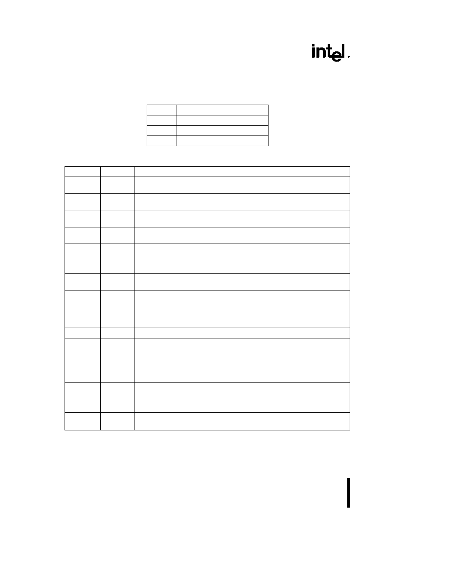
The 82527 pins are described in this section Table 1 presents the legend for interpreting the pin types
Table 1 Pin Type Legend
Symbol
Description
I
Input only pin
O
Output only pin
I O
Pin can be either input or output
PIN DESCRIPTIONS
Pin Name
Pin Type
Pin Description
V
SS1
Ground
GROUND connection must be connected externally to a V
SS
board plane
Provides digital ground
V
SS2
Ground
GROUND connection must be connected externally to a V
SS
board plane
Provides ground for analog comparator
V
CC
Power
POWER connection must be connected externally to a5V DC Provides power
for entire device
XTAL1
I
Input for an external clock XTAL1 (along with XTAL2) are the crystal
connections to an internal oscillator
XTAL2
O
Push-pull output from the internal oscillator XTAL2 (along with XTAL1) are the
crystal connections to an internal oscillator If an external oscillator is used
XTAL2 must be floated or not be connected XTAL2 must not be used as a
clock output to drive other CPUs
CLKOUT
O
Programmable clock output This output may be used to drive the oscillator of
the host microcontroller
RESET
I
Warm Reset (V
CC
remains valid while RESET
is asserted) RESET
must be
driven to a valid low level for 1 ms minimum
Cold Reset (V
CC
is driven to a valid level while RESET
is asserted) RESET
must be driven low for 1 ms minimum measured from a valid V
CC
level No
falling edge on the reset pin is required during a cold reset event
CS
I
A low level on this pin enables CPU access to the 82527 device
INT
O
The interrupt pin is an open-drain output to the host microcontroller V
CC
2 is
the power supply for the ISO low speed physical layer The function of this pin is
(V
CC
2)
O
determined by the MUX bit in the CPU Interface Register (Address 02H) as
follows
MUX e 1 pin 24 (PLCC) e V
CC
2 pin 11 e INT
MUX e 0 pin 24 (PLCC) e INT
RX0
I
Inputs from the CAN bus line(s) to the input comparator A recessive level is
read when RX0
l
RX1 A dominant level is read when RX1
l
RX0 When the
RX1
I
CoBy bit (Bus Configuration register) is programmed as a ``1'' the input
comparator is bypassed and RX0 is the CAN bus line input
TX0
O
Serial data push-pull output to the CAN bus line During a recessive bit TX0 is
high and TX1 is low During a dominant bit TX0 is low and TX1 is high
TX1
O
4

82527
Pin Name
Pin Type
Pin Description
AD0 A0 ICP
I O-I-I
Address Data bus in 8-bit multiplexed mode
AD1 A1 CP
I O-I-I
Address bus in 8-bit non-multiplexed mode
AD2 A2 CSAS
I O-I-I
Low byte of A D bus in 16-bit multiplexed mode
AD3 A3 STE
I O-I
In Serial Interface mode the following pins have the following meaning
AD4 A4 MOSI
I O-I-I
AD0
ICP
Idle Clock Polarity
AD5 A5
I O-I
AD1
CP
Clock Phase
AD6 A6 SCLK
I O-I-I
AD2
CSAS
Chip Select Active State
AD7 A7
I O-I
AD3
STE
Sync Transmit Enable
AD6
SCLK
Serial Clock Input
AD4
MOSI
Serial Data Input
AD8 D0 P1 0
I O-O-I O
High byte of A D bus in 16-bit multiplexed mode
AD9 D1 P1 1
I O-O-I O
Data bus in 8-bit non-multiplexed mode
AD10 D2 P1 2
I O-O-I O
Low speed I O port P1 pins in 8-bit multiplexed mode and serial mode
Port pins have weak pullups until the port is configured by writing to 9FH
AD11 D3 P1 3
I O-O-I O
and AFH
AD12 D4 P1 4
I O-O-I O
AD13 D5 P1 5
I O-O-I O
AD14 D6 P1 6
I O-O-I O
AD15 D7 P1 7
I O-O-I O
P2 0
I O
P2 in all modes
P2 1
I O
P2 6 is INT
when MUX e 1 and is open-drain
P2 2
I O
P2 7 is WRH
in 16-bit multiplexed mode
P2 3
I O
P2 4
I O
P2 5
I O
P2 6 INT
I O-O
P2 7 WRH
I O-I
Mode0
I
These pins select one of the four parallel interfaces These pins are
weakly held low during reset
Mode1
I
Mode1
Mode0
0
0
8-bit multiplexed
Intel
0
0
Serial Interface mode entered when RD
e
0
WR
e
0 upon reset
0
1
16-bit multiplexed
Intel
1
0
8-bit multiplexed
non-Intel
1
1
8-bit non-multiplexed
ALE AS
I-I
ALE used for Intel modes
AS used for non-Intel modes except Mode 3 this pin must be tied high
RD
I
RD
used for Intel modes
E
I
E used for non-Intel modes except Mode 3 Asynchronous this pin must
be tied high
WR
WRL
I
WR
in 8-bit Intel mode and WRL
in 16-bit Intel mode
R W
I
R W
used for non-Intel modes
READY
O
READY is an output to synchronize accesses from the host
microcontroller to the 82527 READY is an open-drain output to the host
MISO
O
microcontroller MISO is the serial data output for the serial interface
mode
DSACK0
O
DSACK0
is an open-drain output to synchronize accesses from the host
microcontroller to the 82527
5