 | –≠–ª–µ–∫—Ç—Ä–æ–Ω–Ω—ã–π –∫–æ–º–ø–æ–Ω–µ–Ω—Ç: 82807AA | –°–∫–∞—á–∞—Ç—å:  PDF PDF  ZIP ZIP |

Intel
‚
‚
‚
‚
82807AA Video Controller Hub
(VCH)
Datasheet
October 2000
Document Reference Number:
290690-001
R

82807AA VCH
2
Datasheet
R
Information in this document is provided in connection with Intel products. No license, express or implied, by estoppel or otherwise, to any intellectual
property rights is granted by this document. Except as provided in Intel's Terms and Conditions of Sale for such products, Intel assumes no liability
whatsoever, and Intel disclaims any express or implied warranty, relating to sale and/or use of Intel products including liability or warranties relating to fitness
for a particular purpose, merchantability, or infringement of any patent, copyright or other intellectual property right. Intel products are not intended for use in
medical, life saving, or life sustaining applications.
Intel may make changes to specifications and product descriptions at any time, without notice.
Designers must not rely on the absence or characteristics of any features or instructions marked "reserved" or "undefined." Intel reserves these for future
definition and shall have no responsibility whatsoever for conflicts or incompatibilities arising from future changes to them.
The Intel
Æ
82807AA VCH may contain design defects or errors known as errata which may cause the product to deviate from published specifications.
Current characterized errata are available on request.
Contact your local Intel sales office or your distributor to obtain the latest specifications and before placing your product order.
I
2
C is a 2-wire communications bus/protocol developed by Philips. SMBus is a subset of the I
2
C bus/protocol and was developed by Intel. Implementations
of the I
2
C bus/protocol may require licenses from various entities, including Philips Electronics N.V. and North American Philips Corporation.
Alert on LAN is a result of the Intel-IBM Advanced Manageability Alliance and a trademark of IBM
Copies of documents which have an ordering number and are referenced in this document, or other Intel literature, may be obtained from:
Intel Corporation
www.intel.com
or call 1-800-548-4725
*Third-party brands and names are the property of their respective owners.
Copyright © Intel Corporation 2000

82807AA VCH
Datasheet
3
R
Contents
1.
Introduction .................................................................................................................................. 9
2.
Product Features........................................................................................................................ 11
3.
Pin Description ........................................................................................................................... 16
3.1.
Notation ......................................................................................................................... 16
3.2.
DVO Interface Signals................................................................................................... 16
3.3.
DVOr Interface Signals.................................................................................................. 17
3.4.
CMOS LCD Interface Signals........................................................................................ 17
3.5.
LVDS LCD Interface Signals ......................................................................................... 18
3.6.
GMBus Signals.............................................................................................................. 18
3.7.
PLL ................................................................................................................................ 19
3.8.
GP I/O Signals............................................................................................................... 19
3.9.
Mvssiscellaneous Signals.............................................................................................. 19
3.10.
82807AA VCH Core Power and Ground ....................................................................... 20
3.11.
Pin States ...................................................................................................................... 21
4.
Interface Description .................................................................................................................. 23
4.1.
DVO to 82807AA VCH .................................................................................................. 23
4.1.1.
Connection .................................................................................................. 23
4.1.2.
DVO Data Format ....................................................................................... 24
4.1.3.
Timing Controls ........................................................................................... 26
4.1.4.
Differential Clocking .................................................................................... 27
4.1.5.
Stalling ........................................................................................................ 27
4.2.
DVOr Interface .............................................................................................................. 28
4.3.
LVDS LCD Interface...................................................................................................... 28
4.3.1.
Clock Pair .................................................................................................... 29
4.3.2.
Data Pair ..................................................................................................... 29
5.
82807AA VCH Basic Operation ................................................................................................. 31
5.1.
82807AA VCH LCD Display Modes .............................................................................. 31
5.1.1.
Normal Mode............................................................................................... 31
5.1.2.
82815EM Centering .................................................................................... 31
5.1.3.
82815EM Panning....................................................................................... 31
5.1.4.
Panel-fitting Mode ....................................................................................... 32
5.1.5.
DVO Bypass Mode...................................................................................... 32
5.2.
GMBus Interface ........................................................................................................... 33
5.2.1.
Base Address .............................................................................................. 33
5.2.2.
Index Address ............................................................................................. 33
5.2.3.
Transfer Format .......................................................................................... 34
6.
Register Description................................................................................................................... 35
6.1.
Register Description ...................................................................................................... 35
6.1.1.
Header ........................................................................................................ 35
6.1.1.1.
VR00 ≠ 82807AA VCH Revision and GMbus Base Address ......... 35
6.1.1.2.
VR01 ≠ 82807AA VCH Functionality Enable .................................. 36
6.1.2.
LCD Interfaces ............................................................................................ 37

82807AA VCH
4
Datasheet
R
6.1.2.1.
VR10 ≠ LCD Interface Format ........................................................37
6.1.2.2.
VR11 ≠ CMOS Output Control ........................................................38
6.1.2.3.
VR12 ≠ LVDS Output Control .........................................................39
6.1.3.
PLL
........................................................................................................39
6.1.3.1.
VR18 ≠ PLL clock select .................................................................40
6.1.3.2.
VR19 ≠ PLL clock divisor ................................................................40
6.1.3.3.
VR1A ≠ PLL clock divisor................................................................40
6.1.4.
Flat Panel Timing.........................................................................................41
6.1.4.1.
VR22 ≠ Horizontal TRP to DE Start Delay ......................................41
6.1.4.2.
VR23 ≠ Horizontal TRP to DE End Delay .......................................41
6.1.4.3.
VR24 ≠ Horizontal TRP to LP Start Delay.......................................41
6.1.4.4.
VR25 ≠ Horizontal TRP to LP End Delay........................................41
6.1.4.5.
VR26 ≠ Vertical TRP to FLM Start Delay ........................................42
6.1.4.6.
VR27 ≠ Vertical TRP to FLM End Delay .........................................42
6.1.5.
Power Sequencing and Panel Protection ....................................................43
6.1.5.1.
VR30 ≠ Panel Power Shut Down Status .........................................43
6.1.5.2.
VR31 ≠ Tpon Panel Power-on Sequencing Delay ..........................43
6.1.5.3.
VR32 ≠ Tpoff Panel Power-off Sequencing Delay .........................44
6.1.5.4.
VR33 ≠ Tstay Panel Power-off Stay Down Delay ..........................44
6.1.5.5.
VR34 ≠ Maximum FLM Pulse Interval ............................................45
6.1.5.6.
VR35 ≠ Maximum LP Pulse Interval ...............................................45
6.1.6.
Panel Fitting .................................................................................................46
6.1.6.1.
VR40 ≠ Panel Fitting Controls.........................................................46
6.1.7.
GPIO
........................................................................................................47
6.1.7.1.
VR80 ≠ GPIO0 Control....................................................................47
6.1.7.2.
VR81 ≠ GPIO1 Control....................................................................47
6.1.7.3.
VR82 ≠ GPIO 2 Control...................................................................48
6.1.7.4.
VR83 ≠ GPIO 3 Control...................................................................48
6.1.7.5.
VR84 ≠ GPIO 4 Control...................................................................48
6.1.7.6.
VR85 ≠ GPIO 5 Control...................................................................49
6.1.7.7.
VR86 ≠ GPIO 6 Control...................................................................50
6.1.7.8.
VR87 ≠ GPIO 7 Control...................................................................51
6.1.7.9.
VR88 ≠ GPIO 8 Control...................................................................51
6.1.8.
Graphics BIOS Scratch Space ....................................................................52
6.1.8.1.
VR8E ≠ Video BIOS Scratch Register 0 .........................................52
6.1.8.2.
VR8F ≠ Video BIOS Scratch Register 1..........................................52
7.
Functional Description ................................................................................................................53
7.1.
Timing Control................................................................................................................53
7.1.1.
Timing Reference Point Generation ............................................................53
7.1.1.1.
Flat Panel Timing Diagram .............................................................53
7.2.
Up Scaling......................................................................................................................55
7.2.1.
Scaling Algorithm .........................................................................................55
7.2.1.1.
Bi-Linear Interpolation .....................................................................55
7.2.1.2.
Multiple Segmented High Order Curve Interpolation ......................56
7.3.
LVDS Transmitter ..........................................................................................................56
7.3.1.
PLL
........................................................................................................56
7.3.1.1.
Serializer With Control ....................................................................56
7.4.
Panel Protection and Power Sequencing.......................................................................57
7.4.1.
Panel Protection...........................................................................................57
7.4.1.1.
Panel Power Sequencing................................................................57
7.5.
DVO Bypassing..............................................................................................................57
7.5.1.
DVOrRCOM.................................................................................................58
7.5.2.
DVO to DVOr Electrical Isolation .................................................................58

82807AA VCH
Datasheet
5
R
7.5.3.
Spread-Spectrum Clocking Support............................................................ 58
7.6.
Power Supply................................................................................................................. 58
7.6.1.
System Connection ..................................................................................... 58
8.
Pinout and Package Information................................................................................................ 61
8.1.
82807AA VCH Pinout .................................................................................................... 61
8.2.
Physical Dimensions ..................................................................................................... 66
9.
External Timing Specifications ................................................................................................... 68
9.1.
Related Documents and References ............................................................................ 69
9.2.
Electrical Characteristics ............................................................................................... 69
9.2.1.
Absolute Maximum DC Ratings .................................................................. 69
9.2.2.
Signal Groups.............................................................................................. 70
9.2.3.
DC Characteristics ...................................................................................... 71
9.2.4.
Ac Characteristics ....................................................................................... 72
9.2.4.1.
Phase Lock Loop Clock Input Timing............................................ 72
9.2.4.2.
Digital Video Out(DVO) Port Interface Timing................................ 72
9.2.5.
82807AA VCH LVDS Switching Characteristics ......................................... 75
9.2.5.1.
CMOS LCD Panel Interface Timing............................................... 76
9.3.
82807AA VCH Timing Diagrams................................................................................... 76
9.3.1.
82807AA VCH LVDS Timing Diagrams ...................................................... 78
9.4.
Power/Thermal Characteristics ..................................................................................... 80
9.4.1.
Power Characteristics ................................................................................. 80
9.4.2.
Thermal Management Introduction ............................................................. 80
9.4.3.
Importance of Thermal Management.......................................................... 80
9.4.3.1.
Thermal Specifications ................................................................... 81
9.4.3.2.
Case Temperature.......................................................................... 81
9.4.3.3.
Measurements for Thermal Specifications ..................................... 81
9.4.3.4.
Case Temperature Measurements................................................. 81
10.
Appendix .................................................................................................................................... 83
10.1.
CMOS LCD Interface Pixel Data Mapping .................................................................... 83
10.2.
LVDS LCD Interface Pixel Data Serial Mapping............................................................ 84

82807AA VCH
6
Datasheet
R
Figures
Figure 1.
Simplified Block Diagram .....................................................................................12
Figure 2.
1.8V DVO Interface ..............................................................................................23
Figure 3.
1.5V DVO Interface ..............................................................................................24
Figure 4.
DVO Clock Data and Control Diagram ................................................................26
Figure 5.
DVO Timing Diagram...........................................................................................27
Figure 6.
Stalling Timing Diagram .......................................................................................28
Figure 7.
LVDS Signaling ....................................................................................................29
Figure 8.
LVDS Clock and Data Diagram ...........................................................................29
Figure 9.
Example of the Format for n Consecutive Register Accessing............................34
Figure 10.
LP and DE With respect to H_TRP......................................................................53
Figure 11.
LP and DE With Respect to V_TRP, H_TRP, and V_DE ....................................54
Figure 12.
FLM With Respect to V_TRP, H_TRP, and LP ...................................................54
Figure 13.
Bi-Linear Interpolation Diagram ...........................................................................55
Figure 14.
Panel Sequencing Diagram .................................................................................57
Figure 15.
Power Plane Diagram ..........................................................................................59
Figure 16.
82807AA VCH Ball Out (Top View-Left Side) ......................................................62
Figure 17.
82807AA VCH Ball Out (Top View-Right Side)....................................................63
Figure 19.
Physical Dimensions Diagram
Top View and Side View.................................66
Figure 20.
Physical Diagrams Dimensions
Bottom View..................................................67
Figure 21.
3.3V Clocking Interface........................................................................................76
Figure 22.
3.3V Clock Duty Cycle..........................................................................................77
Figure 23.
CMOS Panel Out Timing......................................................................................77
Figure 24.
Source Synchronous Digital Video Out Timings ..................................................78
Figure 25.
Channel-to-Channel Skew ...................................................................................78
Figure 26.
LVDS Output Pulse Position Measurements .......................................................79
Figure 27.
Technique for Measuring TCASE With 0∞ Angle Attachment ..............................82
Figure 28.
Technique for Measuring TCASE With 90∞ Angle Attachment ............................82
Tables
Table 1.
Single DVO Data Format .....................................................................................24
Table 2.
Single DVO pixel Data Format .............................................................................25
Table 3.
Single DVO Port System Display Configurations .................................................32
Table 4.
Alphabetical Pin Assignment................................................................................64
Table 6.
82807AA VCH Signal Groups ..............................................................................70
Table 7.
DC Characteristics ...............................................................................................71
Table 8.
LVDS DC Characteristics.....................................................................................72
Table 9.
PLL Clock Timing.................................................................................................72
Table 10.
DVO Port Input Timing: LCD Panel Mode (20-112 MHz)....................................73
Table 11.
DVO Port Input Timing: TV Out Mode .................................................................73
Table 12.
DVOr Port: TV Out Timings .................................................................................73
Table 13.
Data Setup and Hold Times from DVO................................................................74
Table 14.
LVDS Interface Timing Parameters ....................................................................75
Table 15.
CMOS interface Output Timing............................................................................76
Table 16.
Power Characteristics ..........................................................................................80
Table 17.
Thermal Design Power Characteristics................................................................80
Table 18.
Thermal Characteristics .......................................................................................81
Table 19.
CMOS Flat Panel Out ..........................................................................................83
Table 20.
LVDS Conventional Data Mapping for 1x18 Interface .........................................84
Table 21.
LVDS Conventional Data Mapping for 2x18 Interface .........................................84

82807AA VCH
Datasheet
7
R
Table 22.
LVDS Conventional Data Mapping for 1x24 Interface......................................... 85
Table 23.
LVDS Conventional Data Mapping for 2x24 Interface......................................... 86
Table 24.
LVDS Non-Conventional and Conventional Data Mapping ................................. 86
82807AA VCH
8
Datasheet
R
Revision History
Rev.
Description
Date
-001
Initial Release
October 2000

82807AA VCH
Datasheet
9
R
1. Introduction
This document provides design specifications for the Intel
‚
82807AA VCH. It describes I/O interfaces,
registers, and functionality of the chip. This document also includes timing and thermal specifications of
the 82807AA VCH. As a companion chip to the Intel
‚
82815EM, the 82807AA VCH is used in order to
interface an internal TFT LCD used in a notebook PC.

82807AA VCH
10
Datasheet
R

82807AA VCH
Datasheet
11
R
2. Product
Features
LCD Display
∑ Supports TFT panel sizes from SVGA (800x600) up to SXGA+ (1400x1050)
∑ 112 MHz dual channel LVDS LCD interface with Non-Conventional & Conventional formats of:
1x18 or 1x24 for panels with single LVDS channel
2x18 or 2x24 for panels with dual LVDS channels
∑ 36 bit, 3.3v CMOS LCD interface with formats of:
1x18 or 1x24 (Single Pixel per shift clock)
2x18 (Two Pixel per shift clock)
∑ Up-scaling panel fitting with selectable algorithms of
Bi-Linear interpolation
Multiple segmented high order curve approximation interpolation
∑ LVDS transmitter meets TIA/EIA 644 LVDS standard
∑ Spread spectrum clocking
∑ Panel protection during mode switching
∑ Panel power sequencing
Supports DVO bypass on 82807AA VCH DVO replication port to enable:
∑ DVI monitor displaying with an external DVI transmitter
∑ TV displaying with an external TV encoder
Intel
Æ
Digital Video Output (DVO) port specification compliant
ACPI specification compliant
196 Pin pBGA package

82807AA VCH
12
Datasheet
R
Figure 1. Simplified Block Diagram
815EM/VCH Platform
SIO
KBC
Moon
docking
LAN
(Phy)
GMCH
VCH
CRT
LCD
TV
System
Memory
CardBus
FWH
Audio
Modem
Blue
Tooth
HD
CD
DVD
ZIP
Swap
Bay
Smart
Battery
PCI Bus
LPC Bus
AC' Link
USB x4
SM Bus
IDE Ch
DVO
Hub
Interface
I2C
TV Encoder
and/or
DVI Tx
GMBus
DVOr
LVDS or CMOS
CPU
PSB
DVI
Monitor
ICH2-m
NOTE:
The above diagram depicts the 82807AA VCH used in an 815EM platform (single DVO port), for other
platforms this diagram might not apply.

82807AA VCH
Datasheet
13
R
This page left intentionally blank.

82807AA VCH
14
Datasheet
R
Overview
The 82807AA VCH receives display images in RGB pixel format from the 82815EM through a DVO
port. The display image is then converted to the selected LCD panel interface format. The LCD
formatted data can then be accessed from the LVDS interface or CMOS interface.
If needed, the 82807AA VCH is also capable of passing the display image from DVO port through
82807AA VCH to an external TV encoder for TV displaying, or to an external DVI transmitter for DVI
Display support.
All registers in 82807AA VCH are programmed through the 82815EM GMBus, where the 82807AA
VCH is viewed as a child device of the graphics controller in the 82815EM.

82807AA VCH
Datasheet
15
R
This page left intentionally blank

82807AA VCH
16
Datasheet
R
3. Pin
Description
This section provides a detailed description of 82807AA VCH signals. The signals are arranged in
functional groups according to their associated interfaces.
3.1. Notation
The "#" symbol at the end of a signal name indicates that the active, or asserted state occurs when the
signal is at a low voltage level. When "#" is not present after the signal name, the signal is asserted at the
high voltage level.
The following notations are describe the signal type:
I
Input pin
O
Output pin
I/O
Bi-directional Input/Output pin
OD
Open Drain output pin. This pin requires a pull-up to VCC.
I/OD
Input / Open Drain Output pin. This pin requires a pull-up to VCC.
CMOS buffers are used for all of the signals, except LVDS outputs.
The Signal swing voltage is also specified.
3.2.
DVO Interface Signals
Signal Name
Type
Voltage
Description
DVOSTALL/
DVOCLKOUT
O
1.8v
In LCD display mode, if a panel fitting is enabled, this pin
stalls the 82815EM display pipe in line-by-line base. If the
panel fitting is disabled, this pin is driven low.
In the DVO bypassing mode, this pin sends the clock
received from the external TV encoder to the 82815EM. The
maximum frequency is 85 MHz depending on the NTSC or
PAL modes, and the over scan compensation values in the
TV encoder. The worst case duty cycle requirement is 40%
to 60% at the input of the 82815EM.
If 82807AA VCH is driven by a 1.5-V DVO port this pin
(drives 1.8v signaling) will require a voltage *level shifter/or
voltage divider to comply with 1.5v DVO STALL input.
*See appropriate platform guideline for more information.
DVOHSYNC
I
1.8v or 1.5v
DVO horizontal sync input.
DVOVSYNC
I
1.8v or 1.5v
DVO vertical sync input.
DVOBLANK#
I
1.8v or 1.5v
DVO blank input.
DVOCLKIN[1:0]
I
1.8v or 1.5v
DVO differential clock inputs.
Maximum frequency is 112 MHz.
DVODATA[11:0]
I
1.8v or 1.5v
DVO data bus.

82807AA VCH
Datasheet
17
R
3.3.
DVOr Interface Signals
Signal Name
Type
Voltage
Description
DVOrCLKIN
I
1.8 v
In the DVO bypassing mode, if the device on DVOr is a TV
encoder, and it is in master mode, 82807AA VCH receives a clock
from the external TV encoder.
DVOrCLKIN maximum frequency is 85 MHz. The worst case duty
cycle is 60% to 40%.
In the LCD display mode, this input is isolated.
DVOrHSYNC
O
1.8 v
In the DVO bypassing mode, 82807AA VCH passes DVOHSYNC
from 82815EM to the external device on DVOr.
In the LCD display mode, this output is driven low.
DVOrVSYNC
O
1.8 v
In the DVO bypassing mode, 82807AA VCH passes DVOVSYNC
from 82815EM to the external device on DVOr.
In the LCD display mode, this output is driven low.
DVOrBLANK#
O
1.8 v
In the DVO bypassing mode, 82807AA VCH passes DVOBLANK#
from 82815EM to the external device on DVOr.
In the LCD display mode, this output driven low.
DVOrCLKOUT
[1:0]
O
1.8 v
In the DVO bypassing mode, 82807AA VCH passes CLKOUT[1:0]
from 82815EM to the external device on DVOr.
In the LCD display mode, these outputs are driven low.
DVOrDATA
[11:0]
O
1.8 v
In the DVO bypassing mode, 82807AA VCH passes
DVODATA[11:0] from 82815EM to the external device on DVOr.
In the LCD display mode, these outputs are driven low.
DVOrRCOM
I/O
1.8 v
DVOr impedance compensation. Please see specific platform
design guide for resistor values and routing guidelines.
3.4.
CMOS LCD Interface Signals
Signal Name
Type
Voltage
Description
P[35:0]
O
3.3 v
LCD pixel data output. Pixel mapping for different types of LCD
panels is described in the tables in the Pixel Mapping section.
SHFCLK
O
3.3 v
LCD shift clock.
FLM
O
3.3 v
First line mark (equivalent to VSYNC).
LP
O
3.3 v
Latch pulse (equivalent to HSYNC)
DE
O
3.3 v
LCD display enable or BLANK#.

82807AA VCH
18
Datasheet
R
3.5.
LVDS LCD Interface Signals
Signal Name
Type
Voltage
Description
CLKAp
O
1.372-1.028 v
Channel A differential clock pair output (true). 245-800 MHz.
CLKAm
O
1.372-1.028 v
Channel A differential clock pair output (compliment). 245-800
MHz.
YA0p
O
1.372-1.028 v
Channel A differential data pair 0 output (true). 245-800 MHz.
YA0m
O
1.372-1.028 v
Channel A differential data pair 0 output (compliment). 245-800
MHz.
YA1p
O
1.372-1.028 v
Channel A differential data pair 1 output (true). 245-800 MHz.
YA1m
O
1.372-1.028 v
Channel A differential data pair 1 output (compliment). 245-800
MHz.
YA2p
O
1.372-1.028 v
Channel A differential data pair 2 output (true). 245-800 MHz.
YA2m
O
1.372-1.028 v
Channel A differential data pair 2 output (compliment). 245-800
MHz.
YA3p
O
1.372-1.028 v
Channel A differential data pair 3 output (true). 245-800 MHz.
YA3m
O
1.372-1.028 v
Channel A differential data pair 3 output (compliment). 245-800
MHz.
CLKBp
O
1.372-1.028 v
Channel B differential clock pair output (true). 245-800 MHz.
CLKBm
O
1.372-1.028 v
Channel B differential clock pair output (compliment). 245-800
MHz.
YB0p
O
1.372-1.028 v
Channel B differential data pair 0 output (true). 245-800 MHz.
YB0m
O
1.372-1.028 v
Channel B differential data pair 0 output (compliment). 245-800
MHz.
YB1p
O
1.372-1.028 v
Channel B differential data pair 1 output (true). 245-800 MHz.
YB1m
O
1.372-1.028 v
Channel B differential data pair 1 output (compliment). 245-800
MHz.
YB2p
O
1.372-1.028 v
Channel B differential data pair 2 output (true). 245-800 MHz.
YB2m
O
1.372-1.028 v
Channel B differential data pair 2 output (compliment). 245-800
MHz.
YB3p
O
1.372-1.028 v
Channel B differential data pair 3 output (true). 245-800 MHz.
YB3m
O
1.372-1.028 v
Channel B differential data pair 3 output (compliment). 245-800
MHz.
VREF_HI
I
N/A
Test Pin. Needs to be pulled high to 1.8_V
CC
.
VREF_LO
I
N/A
Test Pin. Needs to be pulled low to V
SS
.
3.6. GMBus
Signals
Signal Name
Type
Voltage
Description
GMCK
I
3.3 v
GMBus serial clock
GMDA
I/O D
3.3 v
GMBus serial data

82807AA VCH
Datasheet
19
R
3.7. PLL
Signal Name
Type
Voltage
Description
OSC
I
3.3 v
Core PLL clock reference input. The external clock source is from
the system clock generator with selectable clock frequencies:
either 66 MHz with Spread Spectrum Clocking (SSC), or 48 MHz
without SSC.
3.8.
GP I/O Signals
Signal Name
Type
Voltage
Description
GPIO [8:7]
I/O
OD
3.3 v
Software programmable input/output.
GPIO[8:7] are defaulted to GPIs with their internal pull downs
connected and internal pull ups disconnected.
GPIO[8:7] are used for 82807AA VCH GMBus base address
strapping:
VR00[6] = the value of GPIO[8] at the de-assertion edge of
PCIRST#.
VR00[5] = the value of GPIO[7] at the de-assertion edge of
PCIRST#.
GPIO [6}
I/O
OD
3.3 v
Software programmable input/output.
GPIO[6] is defaulted to GPI with its internal pull down connected
and internal pull up disconnected.
GPIO[6] = 0 at the de-assertion edge of PCIRST#, 82807AA VCH
is in normal operation mode.
GPIO [5:2]
I/O
OD
3.3 v
Software programmable input/output.
GPIO[5:2] are defaulted to GPIs with their internal pull downs
connected and internal pull ups disconnected.
GPIO [1:0]
I/O
OD
3.3 v
Software programmable input/output.
GPIO[1:0] are defaulted to GPOs.
3.9. Mvssiscellaneous
Signals
Signal Name
Type
Voltage
Description
ENAV
DD
O
3.3 v
Power sequencing control for LCD driver electronics voltage
V
DD
.
ENEXBUF
O
3.3 v
LVDS or other data interface enable
ENABKL
O
3.3 v
Power sequencing control for LCD backlight.
TESTIN
I
3.3 v
Test input. When asserted, 82807AA VCH is in Test mode.
PCIRST#
I
3.3 v
Reset for 82807AA VCH. All internal registers and logic are
reset by PCIRST#. The BIOS shall re-initialize 82807AA VCH
interface and all internal 82807AA VCH registers on every
PCIRST#.

82807AA VCH
20
Datasheet
R
3.10.
82807AA VCH Core Power and Ground
Signal Name
Type
Voltage
Description
PLL_V
CC
1.8 v
Core PLL power.
PLL_V
SS
0 v
Core PLL ground
LVDSpll_V
CC
1.8 v
LVDS PLL power
LVDSpll-V
SS
0 v
LVDS PLL ground
LVDSDC_V
CC
1.8 v
LVDS analog circuitry power
LVDSDC_V
SS
0 v
LVDS analog circuitry ground
V
CC
_3.3
3.3v
IO buffer power
V
CC
_1.8
1.8 v
I/O and Core power
V
SS
0 v
Core and I/O ground
LCD_VREF
0.9v or
0.75v
DVO input buffer voltage reference. Please see specific
platform design guide for resistor values and routing guidelines.

82807AA VCH
Datasheet
21
R
3.11. Pin
States
Signal Name
Power
Plane
I/O
At Reset
After
Reset
S0
S1
S3
S4/S5
DVOSTALL/
DVOCLKOUT
1.8 v
output
low
low
per FR100
low
Off
Off
DVOHSYNC
1.8 v or
1.5v
input
driven
driven
driven
Driven(
Off
Off
DVOVSYNC
1.8 v or
1.5v
input
driven
driven
driven
Driven(
Off
Off
DVOBLANK#
1.8 v or
1.5v
input
driven
driven
driven
Driven(
Off
Off
DVOREF
input
0.9V
0.9V
0.9V
0.9V
Off
Off
DVOrCLKIN
1.8 v
input
Gateoff
Gateoff
Per VR10
low
Off
Off
DVOrHSYNC
1.8 v
output
driven
driven
Per VR10
driven
Off
Off
DVOrVSYNC
1.8 v
output
driven
driven
Per VR10
driven
Off
Off
DVOrBLANK#
1.8 v
output
driven
driven
Per VR10
driven
Off
Off
DVOrCLKOUT
[1:0]
1.8 v
output
driven
driven
Per VR10
driven
Off
Off
DVOrDATA[11:0]
1.8 v
output
driven
driven
Per VR10
driven
Off
Off
DVOrRCOM
1.8 v
output
driven
driven
driven
Driven low
Off
Off
P[35:0]
3.3 v
output
low
low
Per VR10
low
Off
Off
SHFCLK
3.3 v
output
low
low
Per VR10
low
Off
Off
FLM
3.3 v
output
low
low
Per VR10
low
Off
Off
LP
3.3 v
output
low
low
Per VR10
low
Off
Off
DE
3.3 v
output
low
low
Per VR10
low
Off
Off
ENAV
DD
3.3 v
output
low
low
Per VR10
low
Off
Off
ENEXBUF
3.3 v
output
low
low
Per VR10
low
Off
Off
ENABKL
3.3 v
output
low
low
Per VR10
low
Off
Off
GMBSCL
3.3 v
Input
Driven
Driven
Driven
Driven
Power off
Power off
GMBSDA
3.3 v
Input
Driven
Driven
Driven
Driven
Power off
Power off
GPIO[8:2]
3.3 v
I/O
I
I
I/OD
I/OD
Off
Off
GPIO [1:0]
3.3 v
I/O
O (low)
O (low)
I/OD
I/OD
Off
Off
TESTIN
3.3 v
I
low
low
low
low
Off
Off
PCIRST#
3.3 v
I
low
high
high
high
low
low
OSC
3.3 v
I
driven
driven
driven
low
Off
Off
LVDSpllV
CC
1.8 v
on
on
on
on
off
off
LVDSdcV
CC
1.8 v
on
on
on
on
off
off
PLLV
CC
1.8 v
on
on
on
on
Off
Off
V
CC
_1.8
1.8 v
-
on
on
on
on
off
off

82807AA VCH
22
Datasheet
R
Signal Name
Power
Plane
I/O
At Reset
After
Reset
S0
S1
S3
S4/S5
V
CC
_3.3
3.3 v
on
on
on
on
off
off

82807AA VCH
Datasheet
23
R
4. Interface
Description
4.1.
DVO to 82807AA VCH
DVO transfers display streams from 82815EM to 82807AA VCH.
4.1.1. Connection
The following diagram indicates the DVO connection between 82815EM and 82807AA VCH.
Figure 2. 1.8V DVO Interface
GMCH
VCH
DVOSTALL/DVICLKIN
DVOSTALL/DVICLKOUT
DVOCLKIN[1:0]
DVOCLKOUT[1:0]
DVODATA[11:0]
DVODATA[11:0]
DVOHSYNC
DVOVSYNC
DVOBLANK#
DVOHSYNC
DVOVSYNC
DVOBLANK#
DVOVREF
DVO
(TVCLKIN/INT#)
(LTVCLKOUT)
(LTVDATA)
(LTVHSYNC)
(LTVVSYNC)
(LTVBLANK)
GMBSDA
GMBSCL
GMBSDA
GMBSCL
GMBus

82807AA VCH
24
Datasheet
R
Figure 3. 1.5V DVO Interface
GMCH
VCH
DVOSTALL/
DV0_FIELD
DVOSTALL/DVICLKOUT
DVOCLKIN[1:0]
DVOCLKOUT[1:0]
DVODATA[11:0]
DVODATA[11:0]
DVOHSYNC
DVOVSYNC
DVOBLANK#
DVOHSYNC
DVOVSYNC
DVOBLANK#
DVOVREF
DVO
GMBSDA
GMBSCL
GMBSDA
GMBSCL
GMBus
*Level
Shifter/
or voltage
divider
*See appropriate platform guidelines for more details
4.1.2.
DVO Data Format
82807AA VCH accepts the DVO, 12-bit, double-pumped, RGB data format where the low half pixel
precedes a high half pixel for LCD displays.
Table 1. Single DVO Data Format
Packet
Clock Edge
DVODATA[11:0]
Low half pixel
Rising Edge
Green[3:0], Blue[7:0]
High half pixel
Falling Edge
Red[7:0], Green[7:4]
82807AA VCH
Datasheet
25
R
The following table below maps a RGB pixel data on the DVODATA[11:0] bus.
Table 2. Single DVO pixel Data Format
Pin Name
Rising edge of CLKIN[0]
Rising edge of CLKIN[1]
DVODATA[0]
B[0]
G[4]
DVODATA[1]
B[1]
G[5]
DVODATA[2]
B[2]
G[6]
DVODATA[3]
B[3]
G[7]
DVODATA[4]
B[4]
R[0]
DVODATA[5]
B[5]
R[1]
DVODATA[6]
B[6]
R[2]
DVODATA[7]
B[7]
R[3]
DVODATA[8]
G[0]
R[4]
DVODATA[9]
G[1]
R[5]
DVODATA[10]
G[2]
R[6]
DVODATA[11]
G[3]
R[7]
Other DVO data formats supported by 82815EM pass from DVO to DVOr without modification. They
are not used for 82807AA VCH LCD displays.
82807AA VCH
26
Datasheet
R
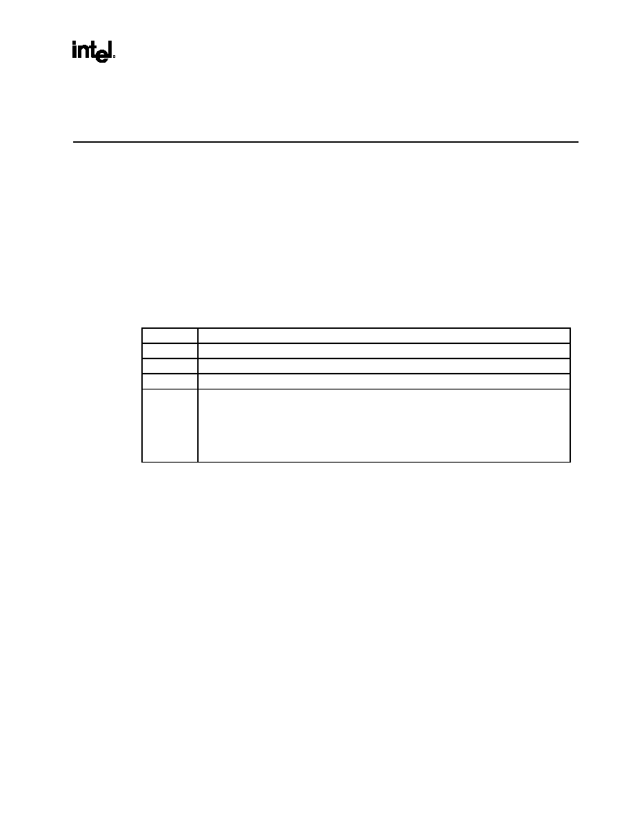
4.1.3. Timing
Controls
DVOBLANK# de-assertion indicates a valid pixel data of a display line. The following diagram is an
example of a display line with 1024 pixels.
Figure 4. DVO Clock Data and Control Diagram
P0
H
P0
L
DVOCLKIN[0]
DVOCLKIN[1]
Invalid
Invalid
.....
.....
DVOBLANK#
P1
H
P1
L
P2
H
P2
L
P1023
H
P1023
L
P1022
H
P1022
L
.....
.....
DVODATA[11:0]
DVOHSYNC signals the beginning of a DVO display line. The number of DVO clocks between two
adjacent DVOHSYNC pulses indicates the H_total of the DVO display line.
DVOVSYNC signals the beginning of a display frame. The number of DVOHSYNC pulses between two
adjacent DVOVSYNC pulses indicates the V_total of the DVO display frame.
The number of DVO clocks of each DVOBLANK# de-asserted period indicates the H_active of the
DVO display line.
The number of DVOBLANK# de-assertions between two adjacent DVOVSYNC pulses indicates the
V_active of the DVO display frame.
The following diagram is an example of DVOBLANK#, DVOHSYNC, and DVOVSYNC in a display
frame of 1024x768 resolution with 807 V_total, including two lines for vertical back-porch blanking and
37 lines for vertical front-porch blanking.

82807AA VCH
Datasheet
27
R
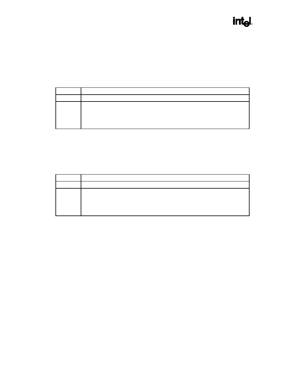
Figure 5. DVO Timing Diagram
DVOHSYNC
DVOVSYNC
line
0
line
1
line
2
line
3
line
768
line
769
line
780
line
781
line
806
line
0
line
1
.....
.....
Frame
n
Frame
n+1
Frame
n-1
V_active
V_blank
V_total
H_total
H_blank (front porch)
V_blank
back porch
front porch
line
2
line
3
.....
H_active
H_blank (back porch)
.....
DVOBLANK#
line
4
line
5
line
805
4.1.4. Differential
Clocking
DVOCLK[1:0] are differential clocks with source synchronous timings. 82807AA VCH uses the cross-
over point between DVOCLK[0] and DVOCLK[1] as the timing reference for latching incoming data.
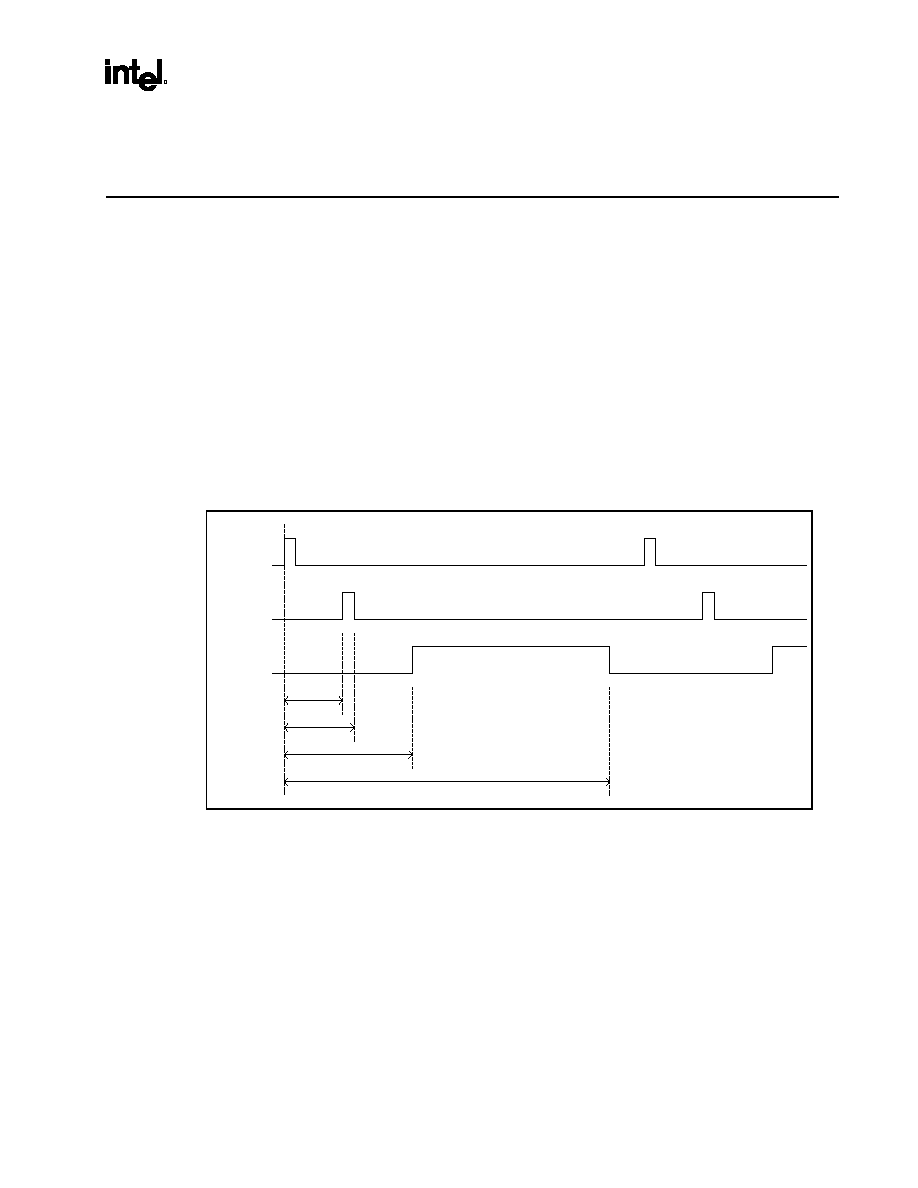
4.1.5. Stalling
DVOSTALL is used by 82807AA VCH to signal to 82815EM for stopping the incoming display stream
in a line by line base. Stalling the DVO stream is a requirement in order to support the 82807AA VCH
up-scaling panel fitting algorithm (see Section 5.1.4).

82807AA VCH
28
Datasheet
R
Figure 6. Stalling Timing Diagram
DVOBLANK#
DVOSTALL
DVODATA
Tstall
setul
DVOHSYNC
line n
line n+1
invalid
DVO H-total
DVO H-active
Tstall
Hold
4.2. DVOr
Interface
DVOr interfaces to a discrete TV encoder, or a discrete DVI transmitter, or an integrated TV encoder
and DVI transmitter.
DVOr protocol and timings are specified in "Intel
Æ
Digital Video Out (DVO) Port" specification.
4.3.
LVDS LCD Interface
There are two LVDS transmitter channels (channel A and channel B) in the 82807AA VCH LVDS LCD
interface. Each channel contains 1 clock pair and 4 data pairs of low voltage differential swing signals.
The following diagram shows a pair of LVDS and their associated swing voltage.

82807AA VCH
Datasheet
29
R
Figure 7. LVDS Signaling
V
a
R
L
=100
V
b
1.425V
0.975V
1.325V
1.075V
"1"
"0"
1.372V
1.028V
Vb
Va
1.20V
450mV
450mV
250mV
250mV
"1"
"0"
344mV
344mV
| Va - Vb |
0.0mV
NOTE:
That 1's and 0's represent the differential voltage between the pair of signals.
VR12[1] enables or disables the LVDS LCD interface. When LVDS LCD interface is disabled, 0's are
output on all LVDS pairs. When the LVDS LCD interface is enabled, the CMOS LCD interface must be
disabled.
The following timing diagram shows a relative relation between LVDS signals and the internal SHFCLK
and pixel data.
Figure 8. LVDS Clock and Data Diagram
4.3.1. Clock
Pair
The SHFCLK frequency is limited to a range from 35 MHz to 112 MHz. A serial pattern of "1100011"
represents 1 cycle of SHFCLK.
4.3.2. Data
Pair
The data pair transfers pixel data and LCD timing control signals. The serial data mapping is specified in
the tables in section 10-1 LVDS LCD Interface Pixel Mapping.
7th
data
1st
data
2nd
data
3rd
data
4th
data
5th
data
6th
data
7th
data
1st
data
1
1
1
0
0
0
1
1
1
LVDS Clock Pair
LVDS Data Pair

82807AA VCH
30
Datasheet
R
This page intentionally left blank.

82807AA VCH
Datasheet
31
R
5.
82807AA VCH Basic Operation
5.1.
82807AA VCH LCD Display Modes
5.1.1. Normal
Mode
When DVO display size (H_active and V_active) is equal to the installed panel size, 82807AA VCH is
in normal operation mode. The 82815EM CRT can be enabled simultaneously with 82807AA VCH in
normal mode.
Panning and centering in 82815EM are used to enable the flexibility of various user display resolutions
(size of display image stored in frame buffer), which may often be different from the installed panel size.
5.1.2. 82815EM
Centering
With centering, the display timings of the DVO port (and CRT if enabled), including DVO clock (dot
clock for CRT) frequency, are set according to the VESA standard at the resolution of installed panel
size, instead of at the user display resolution. DVO (and CRT if enabled) refresh rate is set according to
the installed panel specification (mostly at Vsync=60 Hz). The correct timing setting is the responsibility
of display driver and video BIOS.
Centering is intended for applying to VGA modes due to the necessity of Window OS booting. In the
case of a legacy DOS application changes VGA registers without the involvement of OS and display
driver, the stabilized DVO display size and timings must remain unchanged. The unstable period of DVO
during mode switching is comprehended by 82807AA VCH panel protection function.
5.1.3. 82815EM
Panning
When user display resolution is larger than the installed panel size, panning in 82815EM is used to
equalize the DVO display size to the installed panel size by fetching a portion of the display image from
frame buffer with the size equal to the installed panel size.
If CRT and LCD simultaneous display is enabled, display image is panned on both CRT and LCD.
With panning, the display timings of DVO (and CRT if enabled), including DVO clock (dot clock for
CRT) frequency, are set according to the VESA standard at the resolution of installed panel size, instead
of at the user display resolution. DVO (and CRT if enabled) refresh rate is set according to the installed
panel specification (mostly at 60 Hz). The correct timing setting is the responsibility of display driver.
Panning is not intended for applying to VGA modes due to the installed panel size is not likely to be
smaller than that VGA size.
82807AA VCH
32
Datasheet
R
5.1.4. Panel-fitting
Mode
When DVO display size is smaller than the installed panel size, and panel-fitting function is enabled, the
82807AA VCH is in panel fitting mode.
CRT displaying in 82815EM must be disabled when panel fitting is enabled. Interpolation is used for up
scaling with selectable algorithms of either bi-linear or multiple segmented high order curve
approximation.
Horizontal and vertical scaling ratios are calculated based on installed panel size and DVO display size.
The ratios are used for interpolation weight generation, as well as line stalling generation.
A line based stalling is used in the panel-fitting mode to throttle the incoming stream. The DVOSTALL
signal is multiplexed with the DVOCLKOUT pin at 82807AA VCH DVO interface.
5.1.5.
DVO Bypass Mode
DVO is a point-to-point bus. If there is only one DVO in 82815EM, the DVO is occupied by 82807AA
VCH for LCD displaying in a mobile platform. In order to be able to support TV and DVI displaying,
82807AA VCH DVOr replicates 82815EM DVO to provide a path from 82815EM to a discrete TV
encoder, or a discrete DVI transmitter, or an integrated TV encoder and DVI transmitter. The integrated
TV encoder and DVI transmitter are not expected to operate simultaneously, but can be enabled one at a
time.
DVOr is enabled when 82807AA VCH DVO bypassing is enabled. 82807AA VCH LCD display must be
disabled prior to enabling DVO bypassing.
82807AA VCH PLL is used to generate a 2x DVO clock. The 2x DVO clock is used for DVOr output to
place the clock edge in the middle of the data. 82807AA VCH is also capable of passing TV clock from
the external TV encoder to 82815EM.
Table 3. Single DVO Port System Display Configurations
CRT
82807AA LVDS or CMOS to
Panel
82807AA DVO Bypass (DVOr)
Normal Mode
Normal Mode
Off
Off
Normal Mode
Off
Off
Panel Fitting
Off
Normal Mode
Off
Off
Off
Off
Normal Mode
Normal Mode
Off
Normal Mode
C
onf
igurat
ions
NOTES:
1. Normal Mode includes GMCH Centering and Panning.
2. For Multiple DVO ports, System Display Configurations can be different, see platform guidelines for more details.

82807AA VCH
Datasheet
33
R
5.2. GMBus
Interface
GMBus is used for 82807AA VCH register space accessing. 82807AA VCH GMBus interface supports
up to 400 Kbit/S mode.
82815EM is the only master on this bus. 82807AA VCH operates in slaved mode only.
5.2.1. Base
Address
The 7-bit GMBus base address field of the 82807AA VCH revision, and GMBus base address register
(VR00) determines the base address of 82807AA VCH GMBus. 82807AA VCH GMBus controller will
only respond to a GMBus transfer of which the base address matches the value in the GMBus base
address field of VR00. The user has the ability to strap 82807AA VCH GPIO[8:7] pins in order to select
one of four possible GMBus base addresses (see VR00 register for more description).
5.2.2. Index
Address
An 8-bit index address defines 256 locations of 82807AA VCH register space. Each location contains
16-bit data.
Below are some examples of the index address corresponding to register symbols:
∑ 00h is addressing to register VR00
∑ 01h is addressing to register VR01
∑ 02h is addressing to register VR02
∑ 1Ah is addressing to register VR1A
∑ FFh is addressing to register VRFF
Note: Each VRxx register is 16 bits or 2 bytes of data.

82807AA VCH
34
Datasheet
R
5.2.3. Transfer
Format
Figure 9. Example of the Format for n Consecutive Register Accessing
S
A
Base address
[6:0]
W
index address
[7:0]
A
A
A
Data[7:0]
VRindex
Data[15:8]
VRindex
A
A
Data[7:0]
VRindex+1
Data[15:8]
VRindex+1
...
...
A
A
Data[7:0]
VRindex+n-1
Data[15:8]
VRindex+n-1
S
A
P
START
ACKnowledge
STOP
A#
Not ACKnowledge
R
Read
W
Write
Base address
[6:0]
S
R
A
index address
[7:0]
A
Data[7:0]
VRindex
A
Data[15:8]
VRindex
A
Data[7:0]
VRindex+1
A
Data[15:8]
VRindex+1
A
...
...
Data[7:0]
VRindex+n-1
A
Data[15:8]
VRindex+n-1
A#
P
VCH register Read:
P
VCH register Write:
82807AA VCH
Datasheet
35
R
6. Register
Description
6.1. Register
Description
6.1.1. Header
6.1.1.1.
VR00 ≠ 82807AA VCH Revision and GMbus Base Address
Address offset:
00h
Default:
0002h
Access:
Read only
Bit
Description
15:12
82807AA VCH identification (0h for 82807AA VCH A0)
11:8
82807AA VCH revision number (0h for the first revision of 82807AA VCH A0)
7
Reserved
6:0
82807AA VCH GMBus base address
Possible base addresses are 62h, 42h, 22h or 02h depending on GPIO[8:7] strapping.
VR00[6] = the strapping value of GPIO[8]
VR00[5] = the strapping value of GPIO[7]
VR00[4:0] = 00010b

82807AA VCH
36
Datasheet
R
6.1.1.2.
VR01 ≠ 82807AA VCH Functionality Enable
Address offset:
01h
Default:
0000h
Access:
Read/Write
Bit
Description
15:5
Reserved
4
Reserved
3
Panel Fitting enabled. This bit enables or disables (bypassing) 82807AA VCH panel fitting
function when LCD display is enabled.
0 = disabled
1 = enabled
2
LCD display enabled. This bit enables or disables 82807AA VCH LCD display function.
0 = disabled
1 = enabled
This bit can only be set to 1 if VR01[1] is set to 0, due to there is only one PLL for either LCD
display or DVO bypassing.
1
DVO bypassing enable. This bit enables or disables 82807AA VCH DVOr port.
0 = disabled
1 = enabled
When DVOr is enabled, it repeats the signaling of DVO. When it is disabled, all DVOr outputs are
driven to low, and all DVOr inputs are ignored.
This bit can only be set to 1 if VR01[2] is set to 0, due to there is only one PLL for either LCD
display or DVO bypassing.
0
DVO enable. This bit controls all functions in DVO clock domain by gating the clock of 82807AA
VCH DVO clock domain.
0 = disabled
1 = enabled

82807AA VCH
Datasheet
37
R
6.1.2. LCD
Interfaces
6.1.2.1.
VR10 ≠ LCD Interface Format
Address offset:
10h
Default:
0000h
Access:
Read/Write
Bit
Description
15:5
Reserved
4
LCD interface select.
0 = LVDS disabled, CMOS enabled.
1 = LVDS enabled, CMOS disabled.
Note: there is a desire to split this bit into two bits for driving two panels at the same time.
3:2
Panel interface data width.
00....1x18 bit LVDS
01 1x24 bit LVDS or CMOS (CMOS 1x18 use same MSB's as 1x24 mapping)
10 2x18 bit LVDS or CMOS
11 2x24 bit LVDS
1:0
Panel type.
00 TFT
01 Reserved
10 Reserved
11 Reserved

82807AA VCH
38
Datasheet
R
6.1.2.2.
VR11 ≠ CMOS Output Control
Address offset:
11h
Default:
0000h
Access:
Read/Write
Bit
Description
15
Reserved
14
Shift clock mask.
0 = Allows shift clock output to toggle outside the display enable interval.
1 = Force shift clock output low outside the display enable interval.
13
Force LP during vertical blank.
0 = LP is active during vertical blank time.
1 = LP is inactive during vertical blank time.
12
Force DE during vertical blank.
0 = DE is inactive during vertical blank time.
1 = DE is active during vertical blank time.
11:10
Reserved
9
LCD panel interface group: P[35:0] signals (as a group)
0 = no inversion
1 = invert sense of signal
LCD panel interface group: SHFCLK signal
0 = no inversion
1 = invert sense of signal
7
LCD panel interface group: FLM signal
0 = no inversion
1 = invert sense of signal
6
LCD panel interface group: LP signal
0 = no inversion
1 = invert sense of signal
5
LCD panel interface group: DE signal
0 = no inversion
1 = invert sense of signal
4:2
Reserved
1
LCD timing controls and clock (FLM, LP, DE, and SHFCLK) output buffer strength.
0 = lower drive (12 mA)
1 = higher drive (24 mA)
0
LCD data (P[35:0]) output buffer strength.
0 = lower drive (12 mA)
1 = higher drive (24 mA)
NOTE:
Regardless of the value in VR82, P[35:0], SHFCLK, FLM, LP, and DE will be driven low when ENEXBUF
is asserted.

82807AA VCH
Datasheet
39
R
6.1.2.3.
VR12 ≠ LVDS Output Control
Address offset:
12h
Default:
0080h
Access:
Read/Write
Bit
Description
15:8
Reserved
7:6
LVDS PLL frequency range (Pllrange[1:0])
00 = 35 MHz
01 = 40 MHz
10 = 65 MHz
11 = 108 MHz
5:4
Reserved
3
Data serialization mode
0 = Conventional mode
1 = Non-Conventional mode
2
Second clock pair output control. (En2ndclk)
0 = Disabled
1 = Enabled
1
Software reset to LVDS block.
0 = normal operation
1 = reset the LVDS block
0
LVDS power down control. (drvenslct)
0 = All LVDS pairs are powered up.
1 = Powered down. The pairs not in use will be powered down.
6.1.3. PLL
The three PLL registers are Read/Write with double buffered registers. There are two copies of each of
the three registers. One copy is for SW accessing, and the other copy is for PLL operation. The contents
of the three registers are only transferred from the copy for SW accessing to the copy for PLL operation
is when VR1A is written. And it is required that these registers are programmed in the order of VE18,
VR19, and VR1A. The purpose of the double buffering is for panel protection.

82807AA VCH
40
Datasheet
R
6.1.3.1.
VR18 ≠ PLL clock select
Address offset:
18h
Default:
0010h
Access:
Read/Write with double buffered
Bit
Description
15:0
Reserved
6.1.3.2.
VR19 ≠ PLL clock divisor
Address offset:
19h
Default:
N/A
Access:
Read/Write with double buffered
Bit
Description
15:0
Reserved
6.1.3.3.
VR1A ≠ PLL clock divisor
Address offset:
1Ah
Default:
N/A
Access:
Read/Write with double buffered
Bit
Description
15:0
Reserved

82807AA VCH
Datasheet
41
R
6.1.4.
Flat Panel Timing
6.1.4.1.
VR22 ≠ Horizontal TRP to DE Start Delay
Address offset:
22h
Default:
0000h
Access:
Read/Write
Bit
Description
15:12
Reserved
11:0
Horizontal Timing Reference Point to DE start delay in dot clocks.
6.1.4.2.
VR23 ≠ Horizontal TRP to DE End Delay
Address offset:
23h
Default:
0000h
Access:
Read/Write
Bit
Description
15:0
Reserved
11:0
Horizontal Timing Reference Point to DE end delay in dot clocks.
6.1.4.3.
VR24 ≠ Horizontal TRP to LP Start Delay
Address offset:
24h
Default:
0000h
Access:
Read/Write
Bit
Description
15:12
Reserved
11:0
Horizontal Timing Reference Point to LP Start delay in dot clocks.
6.1.4.4.
VR25 ≠ Horizontal TRP to LP End Delay
Address offset:
25h
Default:
0000h
Access:
Read/Write
Bit
Description
15:12
Reserved
11:0
Horizontal Timing Reference Point to LP End delay in dot clocks.
82807AA VCH
42
Datasheet
R
6.1.4.5.
VR26 ≠ Vertical TRP to FLM Start Delay
Address offset:
26h
Default:
0000h
Access:
Read/Write
Bit
Description
15:12
Reserved
11:0
Vertical Timing Reference Point to FLM Start delay in display lines.
This register specifies the number of lines between V_TRP and FLM Start in vertical direction. In
horizontal direction, FLM is always asserted at the same time as LP pulse assertion. In other
words, FLM is defined in the units of display lines, and LP assertion defines the starting point of
the current display line.
6.1.4.6.
VR27 ≠ Vertical TRP to FLM End Delay
Address offset:
27h
Default:
0000h
Access:
Read/Write
Bit
Description
15:12
Reserved
11:0
Vertical Timing Reference Point to FLM End delay in display lines.
This register specifies the number of lines between V_TRP and FLM End in vertical direction. In
horizontal direction, FLM is always de-asserted at the same time as LP pulse assertion. In other
words, FLM is defined in the units of display lines, and LP assertion also defines the ending point
of the previous display line.

82807AA VCH
Datasheet
43
R
6.1.5.
Power Sequencing and Panel Protection
6.1.5.1.
VR30 ≠ Panel Power Shut Down Status
Address offset:
30h
Default:
0000h
Access:
Read only for [15], Read/write for the rest
Bit
Description
15:15
0 = It is safe to program panel timing and PLL registers in 82807AA VCH. It also indicates panel
powered down sequencing is completed by setting VR01[2] to "0".
1 = It is unsafe to program panel timing and PLL registers in 82807AA VCH.
Note:
This bit is read only.
This bit is set when VR01[2] is set to "1". Software is responsible to enable LCD display by writing
a "1" to VR01[2] after all panel timing and PLL registers are programmed.
This bit is cleared (set to "0") only when VR01[2] has been set to "0" and panel power down
sequencing is completed.
It is also SW responsibility to check this bit before panel timing and PLL registers programming.
14:0
Reserved
6.1.5.2.
VR31 ≠ Tpon Panel Power-on Sequencing Delay
Address offset:
31h
Default:
0200h
Access:
Read/Write
This register controls panel on sequencing delays. The clock source of the power sequencing logic is a
count down of 66 or 48 MHz.
Bit
Description
15:12
Reserved
11:0
Power up delay: Tpon. Programmable value of panel power sequencing delay during power up.
This value can be programmed up to ~256 milliseconds in increments of ~1 millisecond (0.98304
ms actual). A value of 0 is undefined/implementation specific and should be avoided by
programmers.

82807AA VCH
44
Datasheet
R
6.1.5.3.
VR32 ≠ Tpoff Panel Power-off Sequencing Delay
Address offset:
32h
Default:
0200h
Access:
Read/Write
This register controls panel off sequencing delays. The clock source of the power sequencing logic is a
count down of 66 or 48 MHz.
Bit
Description
15:12
Reserved
11:0
Power down delay: Tpoff. Programmable value of panel power sequencing delay during power
down. This value can be programmed up to ~256 milliseconds in increments of ~1 millisecond
(0.98304 ms actual). A value of 0 is undefined/implementation specific and should be avoided by
programmers.
6.1.5.4.
VR33 ≠ Tstay Panel Power-off Stay Down Delay
Address offset:
33h
Default:
0000h
Access:
Read/Write
This register controls how long the panel remains in a power off condition. A few panels limit how fast
the panel may sequence VRom up to down to up again. Typically this is .5-1.5 seconds. This register
forces the panel to stay off. The clock source of the power sequencing logic is a count down of 66 or 48
MHz.
Bit
Description
15:5
Reserved
4:0
Power down delay: Tstay. Programmable value of time panel must remain in a powered down
state. This value can be programmed up to 3.1 seconds in increments of .1 seconds. A value of
0 is no delay.

82807AA VCH
Datasheet
45
R
6.1.5.5.
VR34 ≠ Maximum FLM Pulse Interval
Address offset:
34h
Default:
0001h
Access:
Read/Write
Bit
Description
15
Reserved.
14:0
Maximum FLM pulse interval in display lines.
If no FLM is generated from FPtg when the maximum FLM pulse interval is reached, the
82807AA VCH panel protection state machine generates FLM automatically.
This register is normally programmed to a value, which is less than but close to the maximum
allowance of the installed panel
6.1.5.6.
VR35 ≠ Maximum LP Pulse Interval
Default:
35h
Access:
Read/Write
Bit
Description
15
Reserved.
14:0
Maximum LP pulse interval in dot clocks.
If not, LP is generated from FPtg when the maximum LP pulse interval is reached, the 82807AA
VCH panel protection state machine generates LP automatically.
This register is normally programmed to a value, which is less than but close to the maximum
allowance of the installed panel.

82807AA VCH
46
Datasheet
R
6.1.6. Panel
Fitting
6.1.6.1.
VR40 ≠ Panel Fitting Controls
Address offset:
40h
Default:
0000h
Access:
Read/Write
Bit
Description
15:14
Reserved
13
Stall output enable
0 = disable
1 = enable
12
Vertical interpolation enable
0 = disable
1 = enable
11
Enhanced panel fitting mode enable
0 = disable
1 = enable
10
Horizontal interpolation enable
0 = disable
1 = enable
9
Ratio enable
0 = disable
1 = enable
8
Panel fitting clock gating enable
0 = clock gating is disabled (panel fitting is enabled)
1 = clock gating is enabled (panel fitting is disabled)
7:0
Reserved

82807AA VCH
Datasheet
47
R
6.1.7. GPIO
6.1.7.1.
VR80 ≠ GPIO0 Control
Address offset:
80h,
Default:
0000h
Access:
Read/Write
6.1.7.2.
VR81 ≠ GPIO1 Control
Address offset:
81h,
Default:
0000h
Access:
Read/Write
Bit
VR80,VR81 Description
15:6
Reserved
5
Output inversion
0 = output is not inverted
1 = output is inverted
4
Pull up control
0 = no pull up
1 = 100-Kohm pull up to 3.3V
3
Pull down control
0 = no pull down
1 = 100-Kohm pull down to ground
2
GPIO drive definition
0 = CMOS totem pole outputs
1 = open drain
1
GPIO direction controls
0 = output
1 = input
0
GPIO data
0 = low
1 =high

82807AA VCH
48
Datasheet
R
6.1.7.3.
VR82 ≠ GPIO 2 Control
Address offset:
82h
Default:
0002h
Access:
Read/Write
6.1.7.4.
VR83 ≠ GPIO 3 Control
Address offset:
83h
Default:
0002h
Access:
Read/Write
6.1.7.5.
VR84 ≠ GPIO 4 Control
Address offset:
84h
Default:
0002h
Access:
Read/Write

82807AA VCH
Datasheet
49
R
6.1.7.6.
VR85 ≠ GPIO 5 Control
Address offset:
85h
Default:
0002h
Access:
Read/Write
GPIO[5:2] default to GPI with internal pull down connected at power on reset. Suggested strapping
usage of GPIO[5:2] would be for Panel I.D., with 4 pins used for strapping to allow up to 16 possible
panel types.
Bit
VR82,VR83,VR84, VR85 Description
15:6
Reserved
5
Output inversion
0 = output is not inverted
1 = output is inverted
4
Pull up control
0 = no pull up
1 = 100-Kohm pull up to 3.3V
3
Pull down control
0 = no pull down
1 = 100-Kohm pull down to ground
2
GPIO drive definition
0 = CMOS totem pole outputs
1 = open drain
1
GPIO direction controls
0 = output
1 = input
0
GPIO data
0 = low
1 =high

82807AA VCH
50
Datasheet
R
6.1.7.7.
VR86 ≠ GPIO 6 Control
Address offset:
86h
Default:
0002h
Access:
Read/Write
GPIO[6] default to GPI with internal pull down connected at power on reset.
Note: For 82807AA VCH to be in normal operation mode, GPIO6 must be read as low(0) at the de-assertion
edge of PCIRST#.
Bit
VR86 Description
15:6
Reserved
5
Output inversion
0 = output is not inverted
1 = output is inverted
4
Pull up control
0 = no pull up
1 = 100-Kohm pull up to 3.3V
3
Pull down control
0 = no pull down
1 = 100-Kohm pull down to ground
2
GPIO drive definition
0 = CMOS totem pole outputs
1 = open drain
1
GPIO direction controls
0 = output
1 = input
0
GPIO data
0 = low
1 =high

82807AA VCH
Datasheet
51
R
6.1.7.8.
VR87 ≠ GPIO 7 Control
Address offset:
87h
Default:
0002h
Access:
Read/Write
6.1.7.9.
VR88 ≠ GPIO 8 Control
Address offset:
88h
Default:
0002h
Access:
Read/Write
GPIO[8;7] default to GPI with internal pull down connected at power on reset. The default to GPI for
GPIO[8:7] is used for 82807AA VCH GMBus base address (VR00[6:5]) strapping as follows:
GPIO7=0 at the de-assertion edge of PCIRST#, 82807AA VCH GMBus base address bit 5 (VR00[5]) is
set to 0.
GPIO7=1 at the de-assertion edge of PCIRST#, 82807AA VCH GMBus base address bit 5 (VR00[5]) is
set to 1.
GPIO8=0 at the de-assertion edge of PCIRST#, 82807AA VCH GMBus base address bit 6 (VR00[6]) is
set to 0.
GPIO8=1 at the de-assertion edge of PCIRST#, 82807AA VCH GMBus base address bit 6 (VR00[6]) is
set to 1.
Bit
VR87,VR88 Description
15:6
Reserved
5
Output inversion
0 = output is not inverted
1 = output is inverted
4
Pull up control
0 = no pull up
1 = 100-Kohm pull up to 3.3V
3
Pull down control
0 = no pull down
1 = 100-Kohm pull down to ground
2
GPIO drive definition
0 = CMOS totem pole outputs
1 = open drain
1
GPIO direction controls
0 = output
1 = input
0
GPIO data
0 = low
1 =high

82807AA VCH
52
Datasheet
R
6.1.8.
Graphics BIOS Scratch Space
6.1.8.1.
VR8E ≠ Video BIOS Scratch Register 0
Address offset:
8Eh
Default:
0000h
Access:
Read/Write
Bit
Description
15:0
Graphics BIOS scratch bits
6.1.8.2.
VR8F ≠ Video BIOS Scratch Register 1
Address offset:
8Fh
Default:
0000h
Access:
Read/Write
Bit
Description
15:0
Graphics BIOS scratch bits
82807AA VCH
Datasheet
53
R
7. Functional
Description
7.1. Timing
Control
7.1.1.
Timing Reference Point Generation
DVO timing tracks the X and Y coordinates of a DVO display frames, and generates horizontal and
vertical Timing Reference Point (TRP) according to the DVO X and Y coordinates. DVO timing also
generates vertical display enable (V_DE) by monitoring DVOBLANK#. The horizontal and vertical
TRP, as well as V_DE, are then synchronized to LCD clock domain for FP timing.
7.1.1.1.
Flat Panel Timing Diagram
Figure 10. LP and DE With respect to H_TRP
H_TRP
LP
DE
VR22
VR23
VR24
VR25
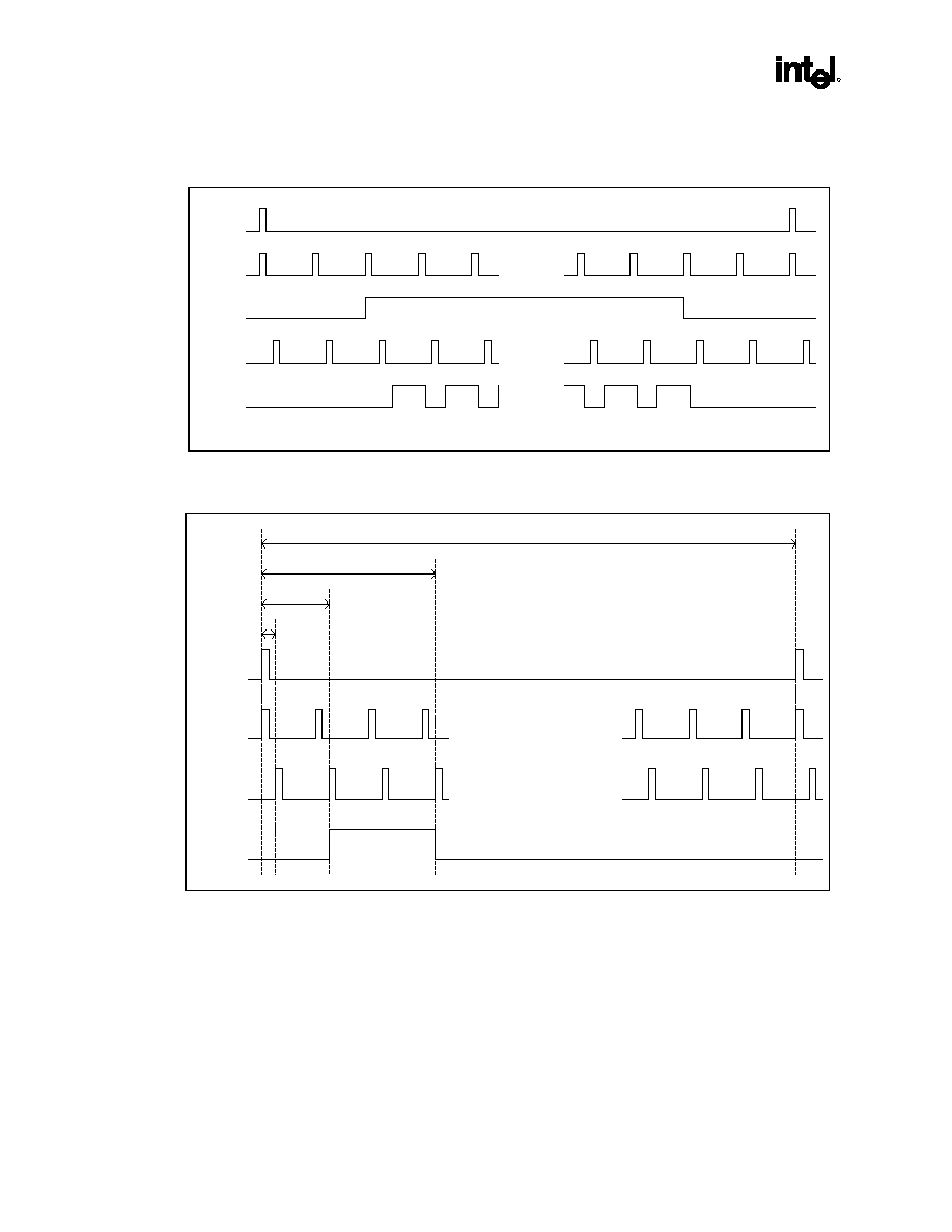
82807AA VCH
54
Datasheet
R
Figure 11. LP and DE With Respect to V_TRP, H_TRP, and V_DE
V_TRP
H_TRP
V_DE
LP
DE
....
....
....
Figure 12. FLM With Respect to V_TRP, H_TRP, and LP
V_total
VR27
VR26
VR22
V_TRP
H_TRP
LP
FLM
....
....
82807AA VCH
Datasheet
55
R
7.2. Up
Scaling
Top left aligned up scaling is supported.
7.2.1. Scaling
Algorithm
Selectable Bi-linear interpolation or multiple-segmented high order curve interpolation scaling
algorithms are used for up scaling function.
7.2.1.1. Bi-Linear
Interpolation
Bi-linear interpolation is to calculate the distance-weighted average of the four neighboring pixels
linearly:
Po(X,Y) = (1-dy) * [(1-dx) * Pi(x,y) + dx * Pi(x+1,y)] + dy * [(1-dx) * Pi(x,y+1) + dx * Pi(x+1,y+1)]
Where:
∑ Po(X,Y) is the calculated pixel output value at (X,Y) coordinates
∑ Pi(x,y) is the input pixel value at (x,y) coordinates
∑ (X,Y) is the output coordinates
∑ (x,y) is the input coordinates
∑ dx is the normalized distance from the output coordinates to the nearest left of the input pixel in horizontal direction
∑ dy is the normalized distance from the output coordinates to the nearest upper of the input pixel in vertical direction
Figure 13. Bi-Linear Interpolation Diagram
Pi(x,y)
Pi(x+1,y)
Pi(x,y+1)
Pi(x+1,y+1)
Po(X,Y)
dx
1-dx
dy
1-dy

82807AA VCH
56
Datasheet
R
7.2.1.2.
Multiple Segmented High Order Curve Interpolation
Scaling with higher order curve algorithm provides better visual quality for deep contrast contents, such
as text, graphics, and video image with sharp edges, etc. This is because the high frequency feature of
the display image requires higher order algorithms to reconstruct. However, higher order algorithm
requires complicated and expensive hardware to realize.
7.3. LVDS
Transmitter
The LVDS (Low Voltage Differential Swing) for LCD flat panels takes a parallel bus and converts it to a
set of high bandwidth serial data streams. Depending on the configuration and mode, it can take 18 bits
of RGB data plus 3 bits of control and output them on three differential outputs; or it can take 24 bits of
RGB data plus 4 bits of control and output it on four differential outputs.
The LVDS supports transmit clock frequency ranges from 35 MHz to 112 MHz, which provides a
throughput of 252 Mbps to 784 Mbps. The phase locked transmit clock is transmitted in parallel with the
data over an additional LVDS channel. The LVDS for flat panel displays is compatible with the
ANSI/TIA/EIA -644-1995 specification.
7.3.1. PLL
The PLL block synthesizes the 7x speed clock required by the high speed serial outputs to set the data
rate of the transmitters. The PLL must also output a synchronized clock at its input clock rate for
transmission over the serial clock line. The frequency of the high speed clock is always 7x it's input.
Since the input clock can operate over a range of 35 MHz to 112 MHz, PLL operation may require a
range switch of at least 1 bit but no more than two bits (4 ranges). There are specific frequencies of
operation that will be likely for LVDS in FPD applications. Those frequencies are 35 MHz, 65 MHz, and
112 MHz. More research is needed to determine the correctness of this information. It is desired that the
common frequencies of operation fall within the center of PLL ranges for best jitter reduction.
7.3.1.1.
Serializer With Control
The serializer block converts 28 bits of parallel data from the graphic controller output into 4 serial data
streams for output on 4 LVDS drivers. A total of four 7-bit wide shift registers are used. The data is
shifted out using a 7x clock generated by the PLL. The registers load in the parallel data from the load
ports using a 1x clock (also generated by the PLL) that is in synchronizes with the 7x clock.
A state machine synchronized to the serial clock generates the load signal. It uses a WAIT state while it
looks for the rising/falling edges of the transmit clock to transit to the WAIT state. The time interval for
the LOAD State is determined by the desired setup/hold time requirement. Upon exiting the LOAD State,
the load signal is asserted for one clock cycle and the SHIFT State starts. The state machine reenters the
WAIT state after 6 cycles and looks again for the edge of the transmit clock.

82807AA VCH
Datasheet
57
R
7.4.
Panel Protection and Power Sequencing
7.4.1. Panel
Protection
When a panel is powered, if the panel timing signals (FLM and LP) are do not toggle after the specified
maximum FLM or LP pulse intervals the panel can be damaged. To prevent this from happening the
82807AA VCH has the ability to assert FLM and LP without DVO H-sync and V-sync.
In 82807AA VCH, LP and FLM signals are generated from the horizontal and vertical TRPs, which are
generated from DVO H-sync and V-sync. When DVO behaves abnormally as the syncs are no longer
toggling, the 82807AA VCH panel protection state machine will automatically assert FLM and LP. The
Maximum FLM pulse interval register (VR34) and the Maximum LP pulse interval register (VR35)
specify the intervals of FLM and LP that are asserted by the panel protection function.
7.4.1.1.
Panel Power Sequencing
The diagram below shows the timing of panel power up and down sequencing.
Figure 14. Panel Sequencing Diagram
PLL_valid
ENAVDD
ENEXBUF
ENABKL
Panel Signaling
Panel Signal
(Data,CLK &
Control)
1 ms
Tpon
Tpoff
Tpoff
Where "Tpon" and "Tpoff" are controlled by the value programmed in VR31 and VR32. Tpon and
Tpoff must satisfy the panel specifications.
7.5. DVO
Bypassing
When the 82807AA VCH Functionality Enable register VR01[1] is set to 1, and the VR01[2] is set to 0,
DVO bypassing mode is enabled.

82807AA VCH
58
Datasheet
R
7.5.1. DVOrRCOM
Please see specific platform design guide for resistor values and routing guidelines for each hub interface
mode.
7.5.2.
DVO to DVOr Electrical Isolation
The 82807AA VCH also provides electrical isolation from the 82815EM DVO to the external TV
encoder or external DVI transmitter. When DVO bypassing is enabled, the LCD display must be
disabled. All circuitry for LCD display are powered down after the panel power-down sequence. When
the DVO bypassing is disabled, all outputs of the DVOr are driven low, and all inputs of the DVOr are
isolated.
7.5.3.
Spread-Spectrum Clocking Support
The 82807AA VCH PLL is capable of locking onto a spread-spectrum referencing clock from the system
clock generator with 0.6% down spreading, while reflecting the spread spectrum in its output. Please
note that the output means both LVDS and Panel signaling. See section 4.7 PLL (OSC) pin description
for more information.
7.6. Power
Supply
7.6.1. System
Connection
The 82807AA VCH has multiple 3.3V and 1.8V power pins. Externally, the 3.3V pins connect to a
single 3.3V supply point, and the 1.8V pins connect to a single 1.8v supply point. The reason for the
multiple dedicated power pins is to provide noise immunity. The separate power pins are not used for
shutting off parts of the chip. In a system, the 3.3V and 1.8V wells in the 82807AA VCH are all
connected to the S3 power plane. A variant of this connection is that the PLL has its own separate 3.3V
regulator for lower noise.
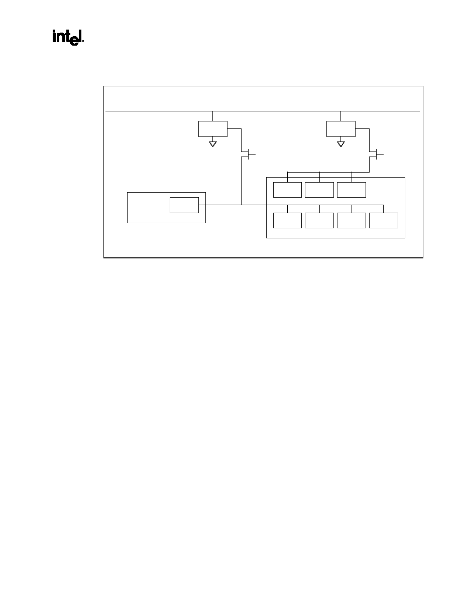
82807AA VCH
Datasheet
59
R
Figure 15. Power Plane Diagram
Raw battery/AC adapter
Unregulated DC 12-18v
(off only during mechanical off)
VCH
I2C
Interface
PLL
LCD
CMOS
Interface
LVDS
DVOr
Interface
DVO
Interface
GMCH
DVO
Interface
1.8v
Regulater
3.3v
Regulater
SLP_S3#
SLP_S3#
VCH
Core
1.8v S3
power plane
3.3v S3
power plane
All S3 power planes are powered during ACPI power states S0-S2. In S3-S5, power is removed.
All dedicated voltage levels in the 82807AA VCH are connected to the S3 power plane in a mobile
platform, and are powered down during S3 to S5.

82807AA VCH
60
Datasheet
R
This page is left intentionally blank.

82807AA VCH
Datasheet
61
R
8.
Pinout and Package Information
8.1.
82807AA VCH Pinout
82807AA VCH Pin Out information contained in Figure 16 and Figure 17

82807AA VCH
62
Datasheet
R
Figure 16. 82807AA VCH Ball Out (Top View-Left Side)
1
2
3
4
5
6
7
A
V
SS
V
CC
3.3
YA0p
YA1p
YA2p
CLKAp
YA3p
B
V
SS
LP
YA0m
YA1m
YA2m
CLKAm
YA3m
C
FLM
ENABKL
ENAV
DD
V
SS
V
CC
1.8
V
CC
3.3
LVDSDC V
CC
D
ENEXBUF
DE
SHFCLK
V
CC
3.3
V
CC
1.8
V
CC
3.3
VREF_LO
E
P2
P1
P0
V
CC
3.3
V
SS
V
SS
V
SS
F
P5
P4
P3
V
CC
1.8
V
SS
V
SS
V
SS
G
P8
P7
P6
V
CC
3.3
V
SS
V
SS
V
SS
H
P11
P10
P9
V
CC
3.3
V
SS
V
SS
V
SS
J
P14
P13
P12
V
CC
3.3
V
SS
V
SS
V
SS
K
P17
P16
P15
V
CC
3.3
V
SS
V
SS
V
SS
L
P20
P19
P18
V
SS
V
CC
1.8
V
CC
3.3
V
CC
1.8
M
P23
P22
P21
P29
P32
P35
DVO DATA9
N
P24
P25
P27
P30
P33
DVO DATA11
DVO DATA8
P
V
SS
P26
P28
P31
P34
DVO DATA10
DVO DATA7
1
2
3
4
5
6
7

82807AA VCH
Datasheet
63
R
Figure 17. 82807AA VCH Ball Out (Top View-Right Side)
8
9
10
11
12
13
14
YB0p
YB1p
YB2p
YB3p
CLKBp
V
CC
3.3
V
SS
A
YB0m
YB1m
YB2m
YB3m
CLKBm
GPIO2
TESTIN
B
LVDSDC V
SS
V
CC
3.3
LVDSpll V
CC
LVDSpll V
SS
GPIO0
GPIO3
GPIO1
C
VREF_HI
V
CC
3.3
V
CC
1.8
V
SS
GMBSCL
GMBSDA
PCIRST
D
V
CC
1.8
V
SS
V
SS
V
CC
1.8
GPIO4
GPIO5
GPIO7
E
V
SS
V
SS
V
SS
V
CC
3.3
GPIO6
GPIO8
DVOr CLKIN F
V
SS
V
SS
V
SS
V
CC
1.8
DVOr
BLANK#
DVOr HSYNC DVOr VSYNC G
V
SS
V
SS
V
SS
V
CC
1.8
DVOr DATA2 DVOr DATA1 DVOr DATA0 H
V
SS
V
SS
V
SS
V
CC
1.8
DVOr
CLKOUT1
DVOr
CLKOUT0
DVOr DATA3 J
V
SS
V
SS
V
SS
V
CC
1.8
DVOr DATA6 DVOr DATA5 DVOr DATA4 K
V
CC
1.8
V
CC
1.8
PLL_V
CC
PLL_V
SS
DVOr DATA9 DVOr DATA8 DVOr DATA7 L
DVOCLKIN0
DVO DATA5
DVO DATA3
DVO DATA0
OSC
DVOrDATA11 DVOrDATA10 M
DVOCLKIN1
DVOr ZCOM
DVO DATA2
DVOBLK#
DVO VSYNC
V
CC
1.8
V
SS
N
DVO DATA6
DVO DATA4
DVO DATA1
DVO HSYNC DVO CLKOUT
LCD VREF
V
SS
P
8
9
10
11
12
13
14

82807AA VCH
64
Datasheet
R
Table 4. Alphabetical Pin Assignment
Signal Name
Ball #
Signal Name
Ball #
Signal Name
Ball #
CLKAm
B6
DVOrDATA3
J14
P10
H2
CLKAp
A6
DVOrDATA4
K14
P11
H1
CLKBm
B12
DVOrDATA5
K13
P12
J3
CLKBp
A12
DVOrDATA6
K12
P13
J2
LVDSDC_V
CC
C7
DVOrDATA7
L14
P14
J1
LVDSDC_V
SS
C8
DVOrDATA8
L13
P15
K3
DE
D2
DVOrDATA9
L12
P16
K2
DVOBLK
N11
DVOrHSYNC
G13
P17
K1
DVOCLKIN0
M8
DVOrVSYC
G14
P18
L3
DVOCLKIN1
N8
DVOrZCOM
N9
P19
L2
DVOCLKOUT
P12
VREF_LO
D7
P2
E1
DVODATA0
M11
VREF_HI
D8
P20
L1
DVODATA1
P10
DVOVSYNC
N12
P21
M3
DVODATA10
P6
ENABKL
C2
P22
M2
DVODATA11
N6
ENAV
DD
C3
P23
M1
DVODATA2
N10
ENEXBUF
D1
P24
N1
DVODATA3
M10
FLM
C1
P25
N2
DVODATA4
P9
GPIO0
C12
P26
P2
DVODATA5
M9
GPIO1
C14
P27
N3
DVODATA6
P8
GMBSDA
D13
P28
P3
DVODATA7
P7
GMBSCL
D12
P29
M4
DVODATA8
N7
GPIO5
E13
P3
F3
DVODATA9
M7
GPIO4
E12
P30
N4
DVOHSYNC
P11
LCDVREF
P13
P31
P4
DVOrBLANK#
G12
GPIO2
B13
P32
M5
DVOrCLKIN
F14
LP
B2
P33
N5
DVOrCLKOUT0
J13
GPIO6
F12
P34
P5
DVOrCLKOUT1
J12
GPIO3
C13
P35
M6
DVOrDATA0
H14
LVDSpll_V
CC
C10
P4
F2
DVOrDATA1
H13
LVDSpll_V
SS
C11
P5
F1
DVOrDATA10
M14
OSC
M12
P6
G3
DVOrDATA11
M13
P0
E3
P7
G2
DVOrDATA2
H12
P1
E2
P8
G1

82807AA VCH
Datasheet
65
R
Table 4. Alphabetical Pin Assignment (cont.)
Signal Name
Ball #
Signal Name
Ball #
Signal Name
Ball #
P9
H3
V
CC
3.3
H4
V
SS
D11
PCIRST
D14
V
CC
3.3
J4
V
SS
F9
PLL_V
CC
L10
V
CC
3.3
K4
V
SS
H8
PLL_V
SS
L11
V
CC
3.3
L6
V
SS
K7
GPIO7
E14
V
SS
E7
V
SS
E5
SHFCLK
D3
V
SS
G7
V
SS
F10
GPIO8
F13
V
SS
J6
V
SS
H9
TESTIN
B14
V
SS
L4
V
SS
K8
V
CC
1.8
C5
V
SS
E9
V
SS
E6
V
CC
1.8
D5
V
SS
G8
V
SS
G5
V
CC
1.8
D10
V
SS
J7
V
SS
H10
V
CC
1.8
E8
V
SS
N14
V
SS
K9
V
CC
1.8
E11
V
SS
E10
V
SS
G6
V
CC
1.8
F4
V
SS
G9
V
SS
J5
V
CC
1.8
G11
V
SS
J8
V
SS
K10
V
CC
1.8
H11
V
SS
P1
YA0m
B3
V
CC
1.8
J11
V
SS
A1
YA0p
A3
V
CC
1.8
K11
V
SS
F5
YA1m
B4
V
CC
1.8
L5
V
SS
G10
YA1p
A4
V
CC
1.8
L7
V
SS
J9
YA2m
B5
V
CC
1.8
L8
V
SS
P14
YA2p
A5
V
CC
1.8
L9
V
SS
A14
YA3m
B7
V
CC
1.8
N13
V
SS
F6
YA3p
A7
V
CC
3.3
A2
V
SS
H5
YB0m
B8
V
CC
3.3
A13
V
SS
J10
YB0p
A8
V
CC
3.3
C6
V
SS
B1
YB1m
B9
V
CC
3.3
C9
V
SS
F7
YB1p
A9
V
CC
3.3
D4
V
SS
H6
YB2m
B10
V
CC
3.3
D6
V
SS
K5
YB2p
A10
V
CC
3.3
D9
V
SS
C4
YB3m
B11
V
CC
3.3
E4
V
SS
F8
YB3p
A11
V
CC
3.3
F11
V
SS
H7
V
CC
3.3
G4
V
SS
K6

82807AA VCH
66
Datasheet
R
8.2. Physical
Dimensions
Figure 18. Physical Dimensions Diagram
Top View and Side View

82807AA VCH
Datasheet
67
R
Figure 19. Physical Diagrams Dimensions
Bottom View

82807AA VCH
68
Datasheet
R
This page is left intentionally ba

82807AA VCH
Datasheet
69
R
External Timing Specifications
8.3.
Related Documents and References
∑ IntelÆ 815EM Design Guide (or other appropriate Design Guide)
- Document Reference Number: 298241
∑ IntelÆ 815EM Chipset: 82815EM Graphics and Memory Controller Hub (GMCH2-M) Datasheet
(or other appropriate Datasheet)
-Document Reference Number: 290689
8.4. Electrical
Characteristics
Unused active low 3.3V tolerant inputs should be connected to 3.3V. Unused active high inputs should
be connected to ground (V
SS
).
8.4.1.
Absolute Maximum DC Ratings
Storage Temperature
-55oC to +150oC
3.3V Supply Voltage with Respect to Vss (V
CC
)
-0.3V to + 3.8V
1.8V Supply Voltage with Respect to Vss
-0.3V to + 2.1V
Warning:
Stressing the device beyond the "Absolute Maximum Ratings" may cause permanent damage. These are
stress ratings only. Operating beyond the "Operating Conditions" is not recommended and extended
exposure beyond "Operating Conditions" may affect reliability.

82807AA VCH
70
Datasheet
R
8.4.2. Signal
Groups
To ease discussion of the AC and DC characteristics, the signals on the 82807AA VCH have been
combined into groups with similar characteristics. These signal groups are referenced throughout this
document.
Table 5. 82807AA VCH Signal Groups
Signal
Group
Signal Type
Signals
(a)
LVDS Output
CLKAp, CLKAm, YA0p, YA0m, YA1p, YA1m, YA2p, YA2m,
YA3p, YA3m, CLKBp, CLKBm, YB0p, YB0m, YB1p, YB1m,
YB2p, YB2m, YB3p, YB3m
(b)
CMOS (3.3V) Input
OSC, TESTIN, PCIRST#
(c)
CMOS (3.3V) Panel Output
P[35:0], SHFCLK, FLM, LP, DE, ENAV
DD
, ENEXBUF, ENABKL
(d)
Digital Video Output Port
Reference Voltage
LCD_VREF
(e)
CMOS (1.8V) I/O
DVOrRCOMP
(f)
CMOS (1.8V) Input
DVOBLANK#, DVODATA[11:0], DVOVSYNC, DVOHSYNC,
DVOCLKIN[1:0], DVOrCLKIN
(g)
CMOS (1.8V) Output
DVOrCLKOUT[1:0], DVOrBLANK#, DVOrDATA[11:0],
DVOrVSYNC, DVOrHSYNC, DVOSTALL/DVOCLKOUT
(h)
CMOS (3.3V) I/O
GMBSCL, GMBSDA
(i)
CMOS I/OD
GPIO[8:0]

82807AA VCH
Datasheet
71
R
8.4.3. DC
Characteristics
Functional Operating Range (Vcc
_1.8
/ LVDSspll_Vcc = 1.80V
±5%, Vcc
_3.3
= 3.3V
±5%; TCASE = 0∞-
95oC).
Table 6. DC Characteristics
Symbol
Sig.Group
Parameter
Min
Max
Unit
Notes
3.3V CMOS I/O Signal DC Characteristics
VIL_3.3
(b,h)
CMOS Input Low Voltage
-0.3
0.8
V
VIH_3.3
(b,h)
CMOS Input High Voltage
2.0
V
sus_3.3
+0.3
V
VOL_3.3
(c,h)
CMOS Output Low Voltage
0.4
V
VOH_3.3
(c,h)
CMOS Output High Voltage
2.4
V
IOL_3.3
(c,h)
CMOS Output Low Current
3
mA
I
LEAK_3.3
(b)
Leakage Current
±10
µA
(c,h)
CMOS Output High Current
-2.0
mA
1.8V CMOS I/O DC Characteristics
VIL_1.8
(f)
CMOS Input Low Voltage
-0.3
0.4(Vcc_
1.8
)
V
VIH_1.8
(f)
CMOS Input High Voltage
0.6(Vcc_
1.8
)
0.3 + (Vcc_
1.8
)
V
VOL_1.8
(g)
CMOS Output Low Voltage
0.1(Vcc_
1.8
)
V
VOH_1.8
(g)
CMOS Output High Voltage
0.9(Vcc_
1.8
)
V
IOL_1.8
(g)
CMOS Output Low Current
1.0
mA
IOH_1.8
(g)
CMOS Output High Current
-1.0
mA
LCD_VREF
(d)
HUBREF voltage reference
0.48(Vcc_
1.8
)
0.52(Vcc_
1.8
)
V
I
LEAK_1.8
(g)
Leakage Current
±10
µA
CMOS I/OD Signal DC Characteristics
VIL_I/OD
(i)
CMOS I/OD Input Low Voltage
0.1
0.8
V
VIH_I/OD
(i)
CMOS I/OD Input High Voltage
2.0
V
sus_3.3
+ 0.1
V
VOL_I/OD
(i)
CMOS I/OD Output Low Voltage
0.4
V
VOH_I/OD
(i)
CMOS I/OD Output High Voltage
2.4
V
IOL_I/OD
(i)
CMOS I/OD Output Low Current
4
mA
I
LEAK_I/OD
(i)
Leakage Current
±100
µA

82807AA VCH
72
Datasheet
R
Functional Operating Range (Vcc
_1.8
/ LVDSspll_Vcc = 1.80V
±5%, Vcc
_3.3
= 3.3V
±5%; TCASE =0∞-
95oC).
Table 7. LVDS DC Characteristics
Symbol
Sig.Group
Parameter
Min
Typ
Max
Unit
Notes
LVDS Driver DC Characteristics
VCM_LVDS
(a)
LVDS Common mode Voltage
1.125 1.25 1.375
V
VCM_LVDS
(a)
LVDS Delta VCM_LVDS
50
mV
VOD_LVDS
(a)
LVDS Differential Output Voltage
250
345
450
mV
VOD_LVDS
(a)
LVDS Delta VOD_LVDS
50
mv
C_LVDS
(a)
LVDS input capacitance
3
pF
NOTE:
R
LOAD
=100
.
8.4.4. Ac
Characteristics
8.4.4.1.
Phase Lock Loop Clock Input Timing
Functional Operating Range (Vcc_1.8
= 1.80V
±5%, V
cc_3.3
= 3.3V
±5%; TCASE =0∞- 95oC).
Table 8. PLL Clock Timing
Symbol
Parameter
48 MHz
66 Mhz
Unit
Notes
OSC (Core PLL clock input)
Typ
Typ
t3a
OSC Period
20.83
15.15
ns
Min
Max
Min
Max
t3b
OSC Jitter
± 300
± 300
t3c
OSC High Time
9.2
5.2
t3d
OSC Low Time
9.2
5.0
t3e
OSC Slew Rate
1.0
4.0
1.0
4.0
t3f
OSC Duty Cycle
45%
55%
45%
55%
8.4.4.2.
Digital Video Out(DVO) Port Interface Timing
All timings are in nanoseconds (ns), unless otherwise specified. In addition, all the clock-to-output values
are specified into 0-pF load, unless otherwise specified.
Functional Operating Range (V
cc_1.8
= 1.80V
±5%, V
cc_3.3
= 3.3V
±5%; TCASE =0∞- 95oC).

82807AA VCH
Datasheet
73
R
Table 9. DVO Port Input Timing: LCD Panel Mode (20-112 MHz)
Symbol
Parameter
Min Max Units Figure
Notes
t4a
DVODATA[11:0], DVOBLANK#, DVOVSYNC, DVOHSYNC valid
before DVOCLKIN[1:0], tTDVb
0.7
ns
23
1
t4b
DVODATA[11:0], DVOBLANK#, DVOVSYNC, DVOHSYNC valid
after DVOCLKIN[1:0], tTDVa
0.9
ns
23
1
Functional Operating Range (V
cc_1.8
= 1.80V
±5%, V
cc_3.3
= 3.3V
±5%; TCASE =0∞- 95oC).
Table 10. DVO Port Input Timing: TV Out Mode
Symbol
Parameter
Min Max Units Figure
Notes
t5a
DVODATA[11:0], DVOBLANK#, DVOVSYNC, DVOHSYNC valid
before DVOCLKIN[1:0], tTDVb
1.7
ns
23
1
t5b
DVODATA[11:0], DVOBLANK#, DVOVSYNC, DVOHSYNC valid
after DVOCLKIN[1:0], tTDVa
1.9
ns
23
1
Functional Operating Range (V
cc_1.8
= 1.80V
±5%, V
cc_3.3
= 3.3V
±5%; TCASE =0∞- 95oC).
Table 11. DVOr Port: TV Out Timings
Symbol
Parameter
Min
Max Units Figure
Notes
t7a
DVOrDATA[11:0], DVOrBLANK#, DVOrVSYNC, DVOrHSYNC valid
before DVOrCLKOUT[1:0], tTDvb
See Table
2-9
ns
23
1
t7b
DVOrDATA[11:0], DVOrBLANK#, DVOrVSYNC, DVOrHSYNC valid
after DVOrCLKOUT[1:0], tTDva
See Table
2-9
ns
23
1
Input Timing
t7c
DVOrCLKIN @ 85 MHz
t7d
DVOrCLKIN Period
11.75
50
ns
t7e
DVVOrCLKIN Jitter
±250
ps
t7f
DVOrCLKIN High Time
3.0
ns
t7g
DVOrCLKIN Low Time
3.0
ns
t7h
DVOrCLKIN Rise Time
0.35
2.0
ns
t7i
DVOrCLKIN Fall Time
0.35
2.0
ns
The output valid delay is measured into a 60-ohm transmission line load and frequency dependent.

82807AA VCH
74
Datasheet
R
Table 12. Data Setup and Hold Times from DVO
DVOrCLKOUT (MHz)
tTDvb
(min)
(ns)
TTDva (min)
(ns)
20
10.75
10.95
25
8.40
8.60
30
6.85
7.05
35
5.74
5.94
40
4.90
5.10
45
4.25
4.45
50
3.73
3.93
55
3.30
3.50
60
2.95
3.15
65
2.65
2.85
70
2.39
2.59
75
2.16
2.36
80
2.01
2.21
85
1.80
2.00
90
1.71
1.91
95
1.58
1.78
100
1.45
1.65
105
1.34
1.54
110
1.24
1.44
112
1.20
1.40
82807AA VCH
Datasheet
75
R
8.4.5.
82807AA VCH LVDS Switching Characteristics
Functional Operating Range (V
cc_1.8
= 1.80V
±5%, V
cc_3.3
= 3.3V
±5%; TCASE =0∞- 95oC).
Table 13. LVDS Interface Timing Parameters
Symbol
Parameter
Min
Typ
Max Units Fig
Notes
Tcs
Channel to Channel Skew
300
ps
25
T9a
Output Skew
-200
0
200
ps
26
1
T9b
Delay time serial bit position 1
1.076 1.276 1.476
ns
26
1
T9c
Delay time serial bit position 2
2.351 2.551 2.751
ns
26
1
T9d
Delay time serial bit position 3
3.626 3.826 4.026
ns
26
1
T9e
Delay time serial bit position 4
4.902 5.102 5.302
ns
26
1
T9f
Delay time serial bit position 5
6.178 6.378 6.578
ns
26
1
T9g
Delay time serial bit position 6
7.453 7.653 7.853
ns
267
1
T9h
Power Down Delay
100
ns
Cycle to Cycle Transmitter Jitter
T9j
F=112 MHz
100
134
ps
T9k
F=65 MHz
175
225
ps
T9m
F=40 MHz
240
380
ps
T9n
F=32.5
260
400
ps
NOTE:
Frequency = 112 MHz.
82807AA VCH
76
Datasheet
R
8.4.5.1.
CMOS LCD Panel Interface Timing
All timings are in nanoseconds (ns), unless otherwise specified. In addition, all the clock-to-output values
are specified into 0 pF load, unless otherwise specified.
Functional Operating Range (V
CC
_1.8
= 1.8V
±5%, V
CC_3.3
/ V
SUS_3.3
= 3.3V
±5%; TCASE =0∞- 95oC)
Table 14. CMOS interface Output Timing
Symbol
Parameter
Min
Max
Units Figure
Notes
t10a
LP, FLM Valid Delay from SFHCLK Rising
-1
3
ns
22
t10b
DE Valid Delay from SFHCLK Rising
-1
3
ns
22
t10c
P[35:0] Valid Delay from SFHCLK Rising
-1
3
ns
22
SHFCLK Timings
t10d
SFHCLK Jitter
250
ps
t10e
SFHCLK Slew Rate
3.4
6.3
V/ns
t10f
SFHCLK Duty Cycle
45
55
%
8.5.
82807AA VCH Timing Diagrams
Figure 20. 3.3V Clocking Interface
SCLK/DVOrCLKIN
DCLKREF
2.0V
0.8V
Period
High Time
Low Time
Fall Time
Rise Time
1.5V
2.0V
0.8V
2.0V
0.8V
1.5V

82807AA VCH
Datasheet
77
R
Figure 21. 3.3V Clock Duty Cycle
Clock
(3.3V)
1.5V
1.5V
Duty Cycle Max
Duty Cycle Min
Figure 22. CMOS Panel Out Timing
SHFCLK
P[35:0]
DE
LP
FLM
Valid Delay
(t
10a-c)

82807AA VCH
78
Datasheet
R
Figure 23. Source Synchronous Digital Video Out Timings
TDVb
TDVa
CLKOUT1
CLKOUT0
DVODATA[11:0]
DVOBLANK
DVOSYNC(H/V)
8.5.1.
82807AA VCH LVDS Timing Diagrams
Figure 24. Channel-to-Channel Skew
Va-Vb=0
Tcs
Y0 (A/B)
Y1(A/B)
Y2 (A/B)
Y3 (A/B)
CLK (A/B)

82807AA VCH
Datasheet
79
R
Figure 25. LVDS Output Pulse Position Measurements
CLK(A/B)
Y(A/B)
T1
T2
T3
T4
T6
T0
T5
Tclk

82807AA VCH
80
Datasheet
R
8.6. Power/Thermal
Characteristics
8.6.1. Power
Characteristics
Table 15. Power Characteristics
Symbol
Parameter
Min
Max
Unit
Notes
Vcc
_1.8
1.8V Core and I/O Supply Voltage
1.71
1.89
V
Vcc
_3.3
3.3V I/O Buffer Supply Voltage
3.15
3.45
V
Vcc
_LVDS_DC_1.8
1.8V LVDS DC Supply Voltage
1.71
1.89
V
PLL_vcc
Core PLL Supply Voltage
1.71
1.89
V
LVDSpll_vcc
LVDS PLL Supply Voltage
1.71
1.89
V
Icc
_1.8
1.8V Core and I/O Supply Current
450
mA
1.
Icc
_3.3
3.3V I/O Buffer Supply Current
100
mA
1.
Icc
_LVDS_DC1.8
1.8V LVDS DC Supply Current
200
uA
1.
Icc
_core_PLL
Core PLL Supply Current
30
mA
1.
Icc_LVDSpll
LVDS PLL 1.8V supply Current
30
mA
1.
NOTES:
1. The maximum values of the currents should not be used to calculate the maximum power consumption, since
they may not occur at the same time.
Table 16. Thermal Design Power Characteristics
Symbol
Configuration
Typ
Unit
Notes
TDP
Typ
LVDS mode
0.6
W
1.
NOTES:
1. TDP
Typ
was estimated based on the configurations listed. TDP
Typ
is the recommended design power. This
number was generated from power estimation, not tested on silicon. Therefore, it is subjected to change.
8.6.2.
Thermal Management Introduction
In a system environment, the chipset temperature is a function of both the system and component thermal
characteristics. The system level thermal constraints consist of the local ambient temperature at the
component, the airflow over the component and surrounding board as well as the physical constraints at,
above and surrounding the component. The component's case temperature depends on the component
power dissipation, size packaging materials (effective thermal conductivity), the type of interconnection
to the substrate and motherboard, the presence of a thermal cooling solution, the thermal conductivity,
the power density of the substrate, and the nearby components and motherboard.
8.6.3.
Importance of Thermal Management
The objective of thermal management is to ensure that the temperatures of all components in a system are
maintained within functional limits. The functional temperature limit is the range within which the
electrical circuits can be expected to meet specified performance requirements. Operation outside the
functional limit can degrade system performance, cause logic errors or cause component and/or system
damage. Temperatures exceeding the maximum operating limits may result in irreversible changes in the
operating characteristics of the component.
82807AA VCH
Datasheet
81
R
8.6.3.1. Thermal
Specifications
To ensure proper operation and reliability of the Intel
Æ
815EM chipset platform, the thermal solution
must maintain a case temperature (T
CASE
) at or below its specified value. Considering the power
dissipation levels and typical system ambient environments of 50
∞C to 70 ∞C, if the 82807AA VCH case
temperature exceeds the maximum case temperature listed in Table 3-3, system or component level
thermal enhancements will be required to dissipate the generated heat. In general, systems should be
designed to dissipate the highest possible thermal power.
Table 17. Thermal Characteristics
Symbol
Parameter
Max
Unit
Notes
T
CASE
Case Temperature
95
∞C
1
NOTE:
1. T
CASE
is defined as the maximum case temperature without any thermal enhancement to the package.
8.6.3.2. Case
Temperature
The case temperature is a function of the local ambient temperature and the internal temperatures of the
Intel
Æ
815EM Chipset platform. As a local ambient temperature is not specified for the Intel
Æ
815EM
Chipset platform, the only restriction is that the maximum case temperature (TCASE) is not exceeded.
Note that increasing the heat flow through the case increases the difference in temperature between the
junction and case, and that reduces the maximum allowable case temperature.
8.6.3.3.
Measurements for Thermal Specifications
Proper measurements must be made to appropriately determine the thermal properties of the system.
Section 8.6.3.4 provides guidelines to accurately measure the case temperature of the Intel
Æ
815EM
Chipset platform.
8.6.3.4.
Case Temperature Measurements
To ensure functionality and reliability, the Intel
Æ
815EM Chipset platform is specified for proper
operation when TCASE is maintained at or below the maximum case temperature listed in Table 17. The
surface temperature of the case in the geometric center of the mold cap is measured. Special care is
required when measuring TCASE to ensure an accurate temperature measurement.
Thermocouples are often used to measure TCASE. Before any temperature measurements are made, the
thermocouples must be calibrated.
When a surface temperature measurement differs from the surrounding local ambient air temperature,
errors could be introduced in the measurements. These measurement errors may result from having a
poor thermal contact between the thermocouple junction and the surface of the package, heat loss by
radiation, convection, by conduction through thermocouple leads, or by contact between the
thermocouple cement and the heat-sink base for heat-sink solutions. To minimize these measurement
errors, the following approach is recommended:
Attaching the Thermocouple:
∑
Use 36 gauge or smaller diameter T type thermocouples.
∑
Ensure that the thermocouple has been properly calibrated.

82807AA VCH
82
Datasheet
R
∑
Attach the thermocouple bead or junction to the top surface of the package (case) in the center of the mold-cap using
high thermal conductivity cements. An alternative for tape attaches users is to use the tape itself to mount the
thermocouple. It is Critical that the thermocouple be closely connected across the entire moldcap.
∑
The thermocouple should be attached at a 0∞ angle if there is no interference with the thermocouple attaches location
or leads. This is the preferred method and is recommended for use with both unenhanced packages as well as packages
employing Thermal Enhancements.
Figure 26. Technique for Measuring TCASE With 0∞ Angle Attachment
∑
If the thermocouple cannot be attached, the thermocouple may be attached at a 90∞ angle.
∑
The hole size through the heat sink base to route the thermocouple wires out should be smaller than 0.150" in
diameter.
∑
Make sure there is no contact between the thermocouple cement and heat sink base. This contact will affect the
thermocouple reading.
Figure 27. Technique for Measuring TCASE With 90∞ Angle Attachment
82807AA VCH
Datasheet
83
R
9. Appendix
9.1.
CMOS LCD Interface Pixel Data Mapping
Table 18 specifies various data formats for the TFT panels.
Table 18. CMOS Flat Panel Out
Pin Name
1x24
2x18
1x18
P0
Bn[0]
Bn[0]
Bn[0]
P1
Bn[1]
Bn[1]
Bn[1]
P2
Bn[2]
Bn[2]
Bn[2]
P3
Bn[3]
Bn[3]
Bn[3]
P4
Bn[4]
Bn[4]
Bn[4]
P5
Bn[5]
Bn[5]
Bn[5]
P6
Bn[6]
Bn+1[0]
P7
Bn[7]
Bn+1[1]
P8
Gn[0]
Bn+1[2]
Gn[0]
P9
Gn[1]
Bn+1[3]
Gn[1]
P10
Gn[2]
Bn+1[4]
Gn[2]
P11
Gn[3]
Bn+1[5]
Gn[3]
P12
Gn[4]
Gn[0]
Gn[4]
P13
Gn[5]
Gn[1]
Gn[5]
P14
Gn[6]
Gn[2]
P15
Gn[7]
Gn[3]
P16
Rn[0]
Gn[4]
Rn[0]
P17
Rn[1]
Gn[5]
Rn[1]
P18
Rn[2]
Gn+1[0]
Rn[2]
P19
Rn[3]
Gn+1[1]
Rn[3]
P20
Rn[4]
Gn+1[2]
Rn[4]
P21
Rn[5]
Gn+1[3]
Rn[5]
P22
Rn[6]
Gn+1[4]
P23
Rn[7]
Gn+1[5]
P24
-
Rn[0]
P25
-
Rn[1]
P26
-
Rn[2]
P27
-
Rn[3]
P28
-
Rn[4]
P29
-
Rn[5]
P30
-
Rn+1[0]
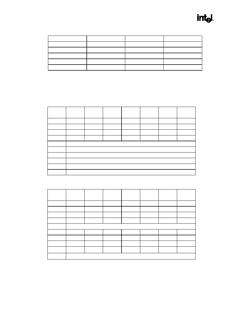
82807AA VCH
84
Datasheet
R
Pin Name
1x24
2x18
1x18
P31
-
Rn+1[1]
P32
-
Rn+1[2]
P33
-
Rn+1[3]
P34
-
Rn+1[4]
P35
-
Rn+1[5]
NOTES:
1. n denotes to nth pixel data.
2. R, G, B denote to the red, green, blue color elements in a pixel and bit 0 is LSB.
9.2.
LVDS LCD Interface Pixel Data Serial Mapping
Table 19. LVDS Conventional Data Mapping for 1x18 Interface
LVDS
Pair
1
st
Data
2
nd
Data
3
rd
Data
4
th
Data
5
th
Data
6
th
Data
7
th
Data
CLKA
1
1
0
0
0
1
1
YA0
Gn[0]
Rn[5]
Rn[4]
Rn[3]
Rn[2]
Rn[1]
Rn[0]
YA1
Bn[1]
Bn[0]
Gn[5]
Gn[4]
Gn[3]
Gn[2]
Gn[1]
YA2
DE
FLM
LP
Bn[5]
Bn[4]
Bn[3]
Bn[2]
YA3
Disabled
CLKB
Disabled
YB0
Disabled
YB1
Disabled
YB2
Disabled
YB3
Disabled
Table 20. LVDS Conventional Data Mapping for 2x18 Interface
LVDS
Pair
1
st
Data
2
nd
Data
3
rd
Data
4
th
Data
5
th
Data
6
th
Data
7
th
Data
CLKA
1
1
0
0
0
1
1
YA0
Gn[0]
Rn[5]
Rn[4]
Rn[3]
Rn[2]
Rn[1]
Rn[0]
YA1
Bn[1]
Bn[0]
Gn[5]
Gn[4]
Gn[3]
Gn[2]
Gn[1]
YA2
DE
FLM
LP
Bn[5]
Bn[4]
Bn[3]
Bn[2]
YA3
Disabled
CLKB
1
1
0
0
0
1
1
YB0
Gn+1[0]
Rn+1[5]
Rn+1[4]
Rn+1[3]
Rn+1[2]
Rn+1[1]
Rn+1[0]
YB1
Bn+1[1]
Bn+1[0]
Gn+1[5]
Gn+1[4]
Gn+1[3]
Gn+1[2]
Gn+1[1]
YB2
0
0
0
Bn+1[5]
Bn+1[4]
Bn+1[3]
Bn+1[2]
YB3
Disabled
NOTES:
1. n denotes to nth pixel data.
2. R, G, B denote to the red, green, blue color elements in a pixel.
3. Based on naming conventions, 18 bpp to 24 bpp are mapped as follows, and bit 0 in each color element is the
LSB of the gray scale.

82807AA VCH
Datasheet
85
R
Table 21. LVDS Conventional Data Mapping for 1x24 Interface
LVDS
Pair
1
st
Data
2
nd
Data
3
rd
Data
4
th
Data
5
th
Data
6
th
Data
7
th
Data
CLKA
1
1
0
0
0
1
1
YA0
Gn[2]
Rn[7]
Rn[6]
Rn[5]
Rn[4]
Rn[3]
Rn[2]
YA1
Bn[3]
Bn[2]
Gn[7]
Gn[6]
Gn[5]
Gn[4]
Gn[3]
YA2
DE
FLM
LP
Bn[7]
Bn[6]
Bn[5]
Bn[4]
YA3
0
Bn[1]
Bn[0]
Gn[1]
Gn[0]
Rn[1]
Rn[0]
CLKB
Disabled
YB0
Disabled
YB1
Disabled
YB2
Disabled
YB3
Disabled

82807AA VCH
86
Datasheet
R
Table 22. LVDS Conventional Data Mapping for 2x24 Interface
LVDS
Pair
1
st
Data
2
nd
Data
3
rd
Data
4
th
Data
5
th
Data
6
th
Data
7
th
Data
CLKA
1
1
0
0
0
1
1
YA0
Gn[2]
Rn[7]
Rn[6]
Rn[5]
Rn[4]
Rn[3]
Rn[2]
YA1
Bn[3]
Bn[2]
Gn[7]
Gn[6]
Gn[5]
Gn[4]
Gn[3]
YA2
DE
FLM
LP
Bn[7]
Bn[6]
Bn[5]
Bn[4]
YA3
0
Bn[1]
Bn[0]
Gn[1]
Gn[0]
Rn[1]
Rn[0]
CLKB
1
1
0
0
0
1
1
YB0
Gn+1[2]
Rn+1[7]
Rn+1[6]
Rn+1[5]
Rn+1[4]
Rn+1[3]
Rn+1[2]
YB1
Bn+1[3]
Bn+1[2]
Gn+1[7]
Gn+1[6]
Gn+1[5]
Gn+1[4]
Gn+1[3]
YB2
0
0
0
Bn+1[7]
Bn+1[6]
Bn+1[5]
Bn+1[4]
YB3
0
Bn+1[1]
Bn+1[0]
Gn+1[1]
Gn+1[0]
Rn+1[1]
Rn+1[0]
Table 23. LVDS Non-Conventional and Conventional Data Mapping
Signal Name
Color Bit Name
24 Bit o/p
18 Bit o/p
48 Bit o/p
36 Bit o/p
CONV
NCON
CONV
NCON
CONV
NCON
CONV
NCON
Channel 0 (YA0)
1st bit
G12
G10
G10
G10
G12
G10
G10
G10
2nd bit
R17
R15
R15
R15
R17
R15
R15
R15
3rd bit
R16
R14
R14
R14
R16
R14
R14
R14
4th bit
R15
R13
R13
R13
R15
R13
R13
R13
5th bit
R14
R12
R12
R12
R14
R12
R12
R12
6th bit
R13
R11
R11
R11
R13
R11
R11
R11
7th bit
R12
R10
R10
R10
R12
R10
R10
R10
Channel 1 (YA1)
1st bit
B13
B11
B11
B11
B13
B11
B11
B11
2nd bit
B12
B10
B10
B10
B12
B10
B10
B10
3rd bit
G17
G15
G15
G15
G17
G15
G15
G15
4th bit
G16
G14
G14
G14
G16
G14
G14
G14
5th bit
G15
G13
G13
G13
G15
G13
G13
G13
6th bit
G14
G12
G12
G12
G14
G12
G12
G12
7th bit
G13
G11
G11
G11
G13
G11
G11
G11
Channel 2 (YA2)
1st bit
DE
DE
DE
DE
DE
DE
DE
DE
2nd bit
VS
VS
VS
VS
VS
VS
VS
VS
3rd bit
HS
HS
HS
HS
HS
HS
HS
HS
4th bit
B17
B15
B15
B15
B17
B15
B15
B15
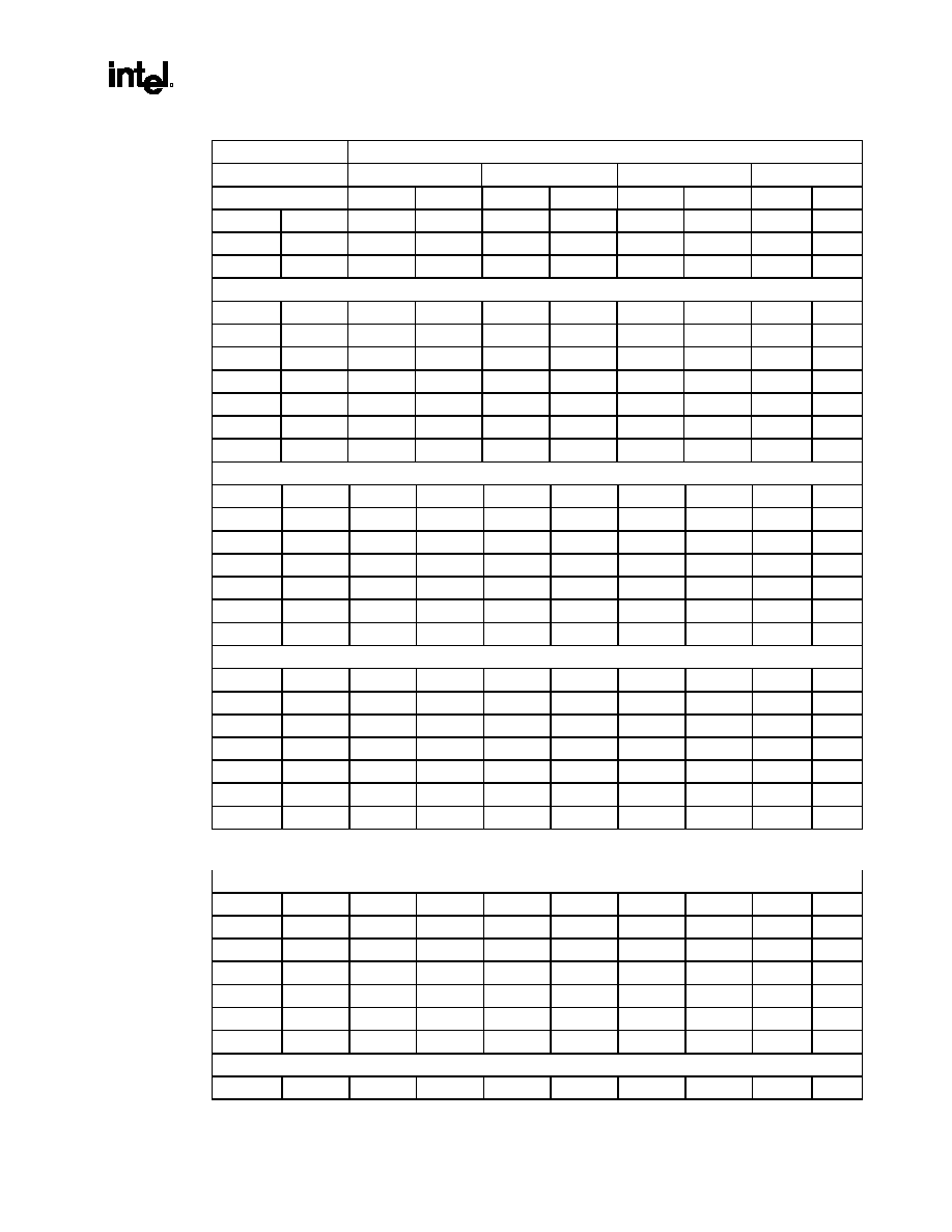
82807AA VCH
Datasheet
87
R
Signal Name
Color Bit Name
24 Bit o/p
18 Bit o/p
48 Bit o/p
36 Bit o/p
CONV
NCON
CONV
NCON
CONV
NCON
CONV
NCON
5th bit
B16
B14
B14
B14
B16
B14
B14
B14
6th bit
B15
B13
B13
B13
B15
B13
B13
B13
7th bit
B14
B12
B12
B12
B14
B12
B12
B12
Channel 3 (YA3)
1st bit
RES
RES
RES
RES
RES
RES
RES
RES
2nd bit
B11
B17
RES
RES
B11
B17
RES
RES
3rd bit
B10
B16
RES
RES
B10
B16
RES
RES
4th bit
G11
G17
RES
RES
G11
G17
RES
RES
5th bit
G10
G16
RES
RES
G10
G16
RES
RES
6th bit
R11
R17
RES
RES
R11
R17
RES
RES
7th bit
R10
R16
RES
RES
R10
R16
RES
RES
Channel 4 (YB0)
1st bit
RES
RES
RES
RES
G22
G20
G20
G20
2nd bit
RES
RES
RES
RES
R27
R25
R25
R25
3rd bit
RES
RES
RES
RES
R26
R24
R24
R24
4th bit
RES
RES
RES
RES
R25
R23
R23
R23
5th bit
RES
RES
RES
RES
R24
R22
R22
R22
6th bit
RES
RES
RES
RES
R23
R21
R21
R21
7th bit
RES
RES
RES
RES
R22
R20
R20
R20
Channel 5 (YB1)
1st bit
RES
RES
RES
RES
B23
B21
B21
B21
2nd bit
RES
RES
RES
RES
B22
B20
B20
B20
3rd bit
RES
RES
RES
RES
G27
G25
G25
G25
4th bit
RES
RES
RES
RES
G26
G24
G24
G24
5th bit
RES
RES
RES
RES
G25
G23
G23
G23
6th bit
RES
RES
RES
RES
G24
G22
G22
G22
7th bit
RES
RES
RES
RES
G23
G21
G21
G21
Channel 6 (YB2)
1st bit
RES
RES
RES
RES
RES
DE
RES
RES
2nd bit
RES
RES
RES
RES
CNTLF
VS
RES
RES
3rd bit
RES
RES
RES
RES
CNTLE
HS
RES
RES
4th bit
RES
RES
RES
RES
B27
B25
B25
B25
5th bit
RES
RES
RES
RES
B26
B24
B24
B24
6th bit
RES
RES
RES
RES
B25
B23
B23
B23
7th bit
RES
RES
RES
RES
B24
B22
B22
B22
Channel 7 (YB3)
1st bit
RES
RES
RES
RES
RES
RES
RES
RES

82807AA VCH
88
Datasheet
R
Signal Name
Color Bit Name
24 Bit o/p
18 Bit o/p
48 Bit o/p
36 Bit o/p
CONV
NCON
CONV
NCON
CONV
NCON
CONV
NCON
2nd bit
RES
RES
RES
RES
B21
B27
RES
RES
3rd bit
RES
RES
RES
RES
B20
B26
RES
RES
4th bit
RES
RES
RES
RES
G21
G27
RES
RES
5th bit
RES
RES
RES
RES
G20
G26
RES
RES
6th bit
RES
RES
RES
RES
R21
R27
RES
RES
7th bit
RES
RES
RES
RES
R20
R26
RES
RES
NOTES:
1. CONV
=
Conventional.
2. NCon
=
Non-Conventional.