 | –≠–ª–µ–∫—Ç—Ä–æ–Ω–Ω—ã–π –∫–æ–º–ø–æ–Ω–µ–Ω—Ç: 82C55A | –°–∫–∞—á–∞—Ç—å:  PDF PDF  ZIP ZIP |
Document Outline
- 82C55A CHMOS PROGRAMMABLE PERIPHERAL INTERFACE
- Pin Description
- 82C55A FUNCTIONAL DESCRIPTION
- General
- Data Bus Buffer
- Read/Write and Control Logic
- Group A and Group B Controls
- Ports A, B, and C
- 82C55A OPERATIONAL DESCRIPTION
- Mode Selection
- Single Bit Set/Reset Feature
- Interrupt Control Functions
- Operating Modes
- MODE 0 (BASIC INPUT)
- MODE 0 (BASIC OUTPUT)
- MODE 0 Port Definition
- MODE 0 Configurations
- MODE 1 (Strobed Input/Output).
- Input Control Signal Definition
- IBF (Input Buffer Full F/F)
- INTR (Interrupt Request)
- Output Control Signal Definition
- Combinations of MODE 1
- MODE 2 (Strobed Bidirectional Bus I/O)
- Bidirectional Bus I/O Control Signal Definition
- Output Operations
- Mode Definition Summary
- Special Mode Combination Considerations
- Current Drive Capability
- Reading Port C Status
- Reading Port C Status
- ABSOLUTE MAXIMUM RATINGS*
- D.C. CHARACTERISTICS
- CAPACITANCE
- A.C. CHARACTERISTICS
- BUS PARAMETERS
- READ CYCLE
- WRITE CYCLE
- OTHER TIMINGS
- WAVEFORMS
- MODE 0 (BASIC INPUT)
- MODE 0 (BASIC OUTPUT)
- MODE 1 (STROBED INPUT)
- MODE 1 (STROBED OUTPUT)
- MODE 2 (BIDIRECTIONAL)
- WRITE TIMING
- READ TIMING
- A.C. TESTING INPUT, OUTPUT WAVEFORM
- A.C. TESTING LOAD CIRCUIT

October 1995
Order Number 231256-004
82C55A
CHMOS PROGRAMMABLE PERIPHERAL INTERFACE
Y
Compatible with all Intel and Most
Other Microprocessors
Y
High Speed ``Zero Wait State''
Operation with 8 MHz 8086 88 and
80186 188
Y
24 Programmable I O Pins
Y
Low Power CHMOS
Y
Completely TTL Compatible
Y
Control Word Read-Back Capability
Y
Direct Bit Set Reset Capability
Y
2 5 mA DC Drive Capability on all I O
Port Outputs
Y
Available in 40-Pin DIP and 44-Pin PLCC
Y
Available in EXPRESS
Standard Temperature Range
Extended Temperature Range
The Intel 82C55A is a high-performance CHMOS version of the industry standard 8255A general purpose
programmable I O device which is designed for use with all Intel and most other microprocessors It provides
24 I O pins which may be individually programmed in 2 groups of 12 and used in 3 major modes of operation
The 82C55A is pin compatible with the NMOS 8255A and 8255A-5
In MODE 0 each group of 12 I O pins may be programmed in sets of 4 and 8 to be inputs or outputs In
MODE 1 each group may be programmed to have 8 lines of input or output 3 of the remaining 4 pins are used
for handshaking and interrupt control signals MODE 2 is a strobed bi-directional bus configuration
The 82C55A is fabricated on Intel's advanced CHMOS III technology which provides low power consumption
with performance equal to or greater than the equivalent NMOS product The 82C55A is available in 40-pin
DIP and 44-pin plastic leaded chip carrier (PLCC) packages
231256 ≠ 1
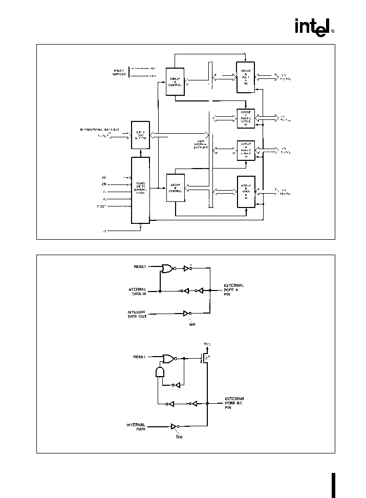
Figure 1 82C55A Block Diagram
231256 ≠ 31
231256 ≠ 2
Figure 2 82C55A Pinout
Diagrams are for pin reference only Package
sizes are not to scale

82C55A
Table 1 Pin Description
Symbol
Pin Number
Type
Name and Function
Dip
PLCC
PA
3≠0
1 ≠ 4
2 ≠ 5
I O
PORT A PINS 0 ≠ 3
Lower nibble of an 8-bit data output latch
buffer and an 8-bit data input latch
RD
5
6
I
READ CONTROL
This input is low during CPU read operations
CS
6
7
I
CHIP SELECT
A low on this input enables the 82C55A to
respond to RD and WR signals RD and WR are ignored
otherwise
GND
7
8
System Ground
A
1≠0
8 ≠ 9
9 ≠ 10
I
ADDRESS
These input signals in conjunction RD and WR
control the selection of one of the three ports or the control
word registers
A
1
A
0
RD
WR
CS
Input Operation (Read)
0
0
0
1
0
Port A - Data Bus
0
1
0
1
0
Port B - Data Bus
1
0
0
1
0
Port C - Data Bus
1
1
0
1
0
Control Word - Data Bus
Output Operation (Write)
0
0
1
0
0
Data Bus - Port A
0
1
1
0
0
Data Bus - Port B
1
0
1
0
0
Data Bus - Port C
1
1
1
0
0
Data Bus - Control
Disable Function
X
X
X
X
1
Data Bus - 3 - State
X
X
1
1
0
Data Bus - 3 - State
PC
7≠4
10 ≠ 13
11 13 ≠ 15
I O
PORT C PINS 4 ≠ 7
Upper nibble of an 8-bit data output latch
buffer and an 8-bit data input buffer (no latch for input) This port
can be divided into two 4-bit ports under the mode control Each
4-bit port contains a 4-bit latch and it can be used for the control
signal outputs and status signal inputs in conjunction with ports
A and B
PC
0≠3
14 ≠ 17
16 ≠ 19
I O
PORT C PINS 0 ≠ 3
Lower nibble of Port C
PB
0-7
18 ≠ 25
20 ≠ 22
I O
PORT B PINS 0 ≠ 7
An 8-bit data output latch buffer and an 8-
24 ≠ 28
bit data input buffer
V
CC
26
29
SYSTEM POWER a
5V Power Supply
D
7≠0
27 ≠ 34
30 ≠ 33
I O
DATA BUS
Bi-directional tri-state data bus lines connected to
35 ≠ 38
system data bus
RESET
35
39
I
RESET
A high on this input clears the control register and all
ports are set to the input mode
WR
36
40
I
WRITE CONTROL
This input is low during CPU write
operations
PA
7≠4
37 ≠ 40
41 ≠ 44
I O
PORT A PINS 4 ≠ 7
Upper nibble of an 8-bit data output latch
buffer and an 8-bit data input latch
NC
1 12
No Connect
23 34
2

82C55A
82C55A FUNCTIONAL DESCRIPTION
General
The 82C55A is a programmable peripheral interface
device designed for use in Intel microcomputer sys-
tems Its function is that of a general purpose I O
component to interface peripheral equipment to the
microcomputer system bus The functional configu-
ration of the 82C55A is programmed by the system
software so that normally no external logic is neces-
sary to interface peripheral devices or structures
Data Bus Buffer
This 3-state bidirectional 8-bit buffer is used to inter-
face the 82C55A to the system data bus Data is
transmitted or received by the buffer upon execution
of input or output instructions by the CPU Control
words and status information are also transferred
through the data bus buffer
Read Write and Control Logic
The function of this block is to manage all of the
internal and external transfers of both Data and
Control or Status words It accepts inputs from the
CPU Address and Control busses and in turn issues
commands to both of the Control Groups
Group A and Group B Controls
The functional configuration of each port is pro-
grammed by the systems software In essence the
CPU ``outputs'' a control word to the 82C55A The
control word contains information such as ``mode''
``bit set'' ``bit reset'' etc
that initializes the func-
tional configuration of the 82C55A
Each of the Control blocks (Group A and Group B)
accepts ``commands'' from the Read Write Control
Logic receives ``control words'' from the internal
data bus and issues the proper commands to its as-
sociated ports
Control Group A - Port A and Port C upper (C7 ≠ C4)
Control Group B - Port B and Port C lower (C3 ≠ C0)
The control word register can be both written and
read as shown in the address decode table in the
pin descriptions Figure 6 shows the control word
format for both Read and Write operations When
the control word is read bit D7 will always be a logic
``1'' as this implies control word mode information
Ports A B and C
The 82C55A contains three 8-bit ports (A B and C)
All can be configured in a wide variety of functional
characteristics by the system software but each has
its own special features or ``personality'' to further
enhance the power and flexibility of the 82C55A
Port A
One 8-bit data output latch buffer and one
8-bit input latch buffer Both ``pull-up'' and ``pull-
down'' bus hold devices are present on Port A
Port B
One 8-bit data input output latch buffer
Only ``pull-up'' bus hold devices are present on Port
B
Port C
One 8-bit data output latch buffer and one
8-bit data input buffer (no latch for input) This port
can be divided into two 4-bit ports under the mode
control Each 4-bit port contains a 4-bit latch and it
can be used for the control signal outputs and status
signal inputs in conjunction with ports A and B Only
``pull-up'' bus hold devices are present on Port C
See Figure 4 for the bus-hold circuit configuration for
Port A B and C
3
82C55A
231256 ≠ 3
Figure 3 82C55A Block Diagram Showing Data Bus Buffer and Read Write Control Logic Functions
NOTE
231256 ≠ 4
Port pins loaded with more than 20 pF capacitance may not have their logic level guaranteed following a hardware reset
Figure 4 Port A B C Bus-hold Configuration
4

82C55A
82C55A OPERATIONAL DESCRIPTION
Mode Selection
There are three basic modes of operation that can
be selected by the system software
Mode 0
Basic input output
Mode 1
Strobed Input output
Mode 2
Bi-directional Bus
When the reset input goes ``high'' all ports will be set
to the input mode with all 24 port lines held at a logic
``one'' level by the internal bus hold devices (see
Figure 4 Note) After the reset is removed the
82C55A can remain in the input mode with no addi-
tional initialization required This eliminates the need
for pullup or pulldown devices in ``all CMOS'' de-
signs During the execution of the system program
any of the other modes may be selected by using a
single output instruction
This allows a single
82C55A to service a variety of peripheral devices
with a simple software maintenance routine
The modes for Port A and Port B can be separately
defined while Port C is divided into two portions as
required by the Port A and Port B definitions All of
the output registers including the status flip-flops
will be reset whenever the mode is changed Modes
may be combined so that their functional definition
can be ``tailored'' to almost any I O structure For
instance Group B can be programmed in Mode 0 to
monitor simple switch closings or display computa-
tional results Group A could be programmed in
Mode 1 to monitor a keyboard or tape reader on an
interrupt-driven basis
231256 ≠ 5
Figure 5 Basic Mode Definitions and Bus
Interface
231256 ≠ 6
Figure 6 Mode Definition Format
The mode definitions and possible mode combina-
tions may seem confusing at first but after a cursory
review of the complete device operation a simple
logical I O approach will surface The design of the
82C55A has taken into account things such as effi-
cient PC board layout control signal definition vs PC
layout and complete functional flexibility to support
almost any peripheral device with no external logic
Such design represents the maximum use of the
available pins
Single Bit Set Reset Feature
Any of the eight bits of Port C can be Set or Reset
using a single OUTput instruction This feature re-
duces software requirements in Control-based appli-
cations
When Port C is being used as status control for Port
A or B these bits can be set or reset by using the Bit
Set Reset operation just as if they were data output
ports
5