 | –≠–Ľ–Ķ–ļ—ā—Ä–ĺ–Ĺ–Ĺ—č–Ļ –ļ–ĺ–ľ–Ņ–ĺ–Ĺ–Ķ–Ĺ—ā: 845E | –°–ļ–į—á–į—ā—Ć:  PDF PDF  ZIP ZIP |

Intel
ģ
845E Chipset
Datasheet
Intel
ģ
82845 Memory Controller Hub (MCH) for DDR
May 2002
Document Number:
290742-001
R

R
2
Intel
ģ
82845 MCH Datasheet
Information in this document is provided in connection with Intel
ģ
products. No license, express or implied, by estoppel or otherwise, to any intellectual
property rights is granted by this document. Except as provided in Intel's Terms and Conditions of Sale for such products, Intel assumes no liability
whatsoever, and Intel disclaims any express or implied warranty, relating to sale and/or use of Intel products including liability or warranties relating to
fitness for a particular purpose, merchantability, or infringement of any patent, copyright or other intellectual property right. Intel products are not
intended for use in medical, life saving, or life sustaining applications.
Intel may make changes to specifications and product descriptions at any time, without notice.
Designers must not rely on the absence or characteristics of any features or instructions marked "reserved" or "undefined." Intel reserves these for
future definition and shall have no responsibility whatsoever for conflicts or incompatibilities arising from future changes to them.
The Intel
ģ
845E chipset may contain design defects or errors known as errata which may cause the product to deviate from published specifications.
Current characterized errata are available on request.
Contact your local Intel sales office or your distributor to obtain the latest specifications and before placing your product order.
I
2
C is a two-wire communications bus/protocol developed by Philips. SMBus is a subset of the I
2
C bus/protocol and was developed by Intel.
Implementations of the I
2
C bus/protocol may require licenses from various entities, including Philips Electronics N.V. and North American Philips
Corporation.
Alert on LAN is a result of the Intel-IBM Advanced Manageability Alliance and a trademark of IBM.
Intel, Pentium, and the Intel logo are trademarks or registered trademarks of Intel Corporation or its subsidiaries in the United States and other
countries.
*Other names and brands may be claimed as the property of others.
Copyright © 2002, Intel Corporation

R
Intel
ģ
82845 MCH Datasheet
3
Contents
1
Introduction ........................................................................................................................11
1.1
Terminology and Notations ...................................................................................11
1.2
Reference Documents ..........................................................................................13
1.3
Intel
ģ
845E Chipset System Architecture..............................................................14
1.4
Intel
ģ
82845 MCH Overview .................................................................................14
1.4.1
System Bus Interface ............................................................................15
1.4.2
System Bus Error Checking ..................................................................15
1.4.3
System Memory Interface .....................................................................16
1.4.4
AGP Interface........................................................................................16
1.4.5
Hub Interface.........................................................................................17
1.4.6
MCH Clocking .......................................................................................17
1.4.7
System Interrupts ..................................................................................18
1.4.8
Powerdown Flow ...................................................................................18
2
Signal Description..............................................................................................................19
2.1
System Bus Signals ..............................................................................................21
2.2
DDR SDRAM Interface Signals ............................................................................23
2.3
Hub Interface Signals............................................................................................24
2.4
AGP Interface Signals...........................................................................................24
2.4.1
AGP Addressing Signals .......................................................................24
2.4.2
AGP Flow Control Signals .....................................................................25
2.4.3
AGP Status Signals ...............................................................................25
2.4.4
AGP Strobes Signals.............................................................................26
2.4.5
AGP/PCI Signals ...................................................................................26
2.5
Clocks, Reset, and Miscellaneous Signals ...........................................................28
2.6
Voltage Reference and Power Signals .................................................................29
2.7
Pin States during Reset ........................................................................................30
3
Register Description ..........................................................................................................31
3.1
Register Terminology............................................................................................31
3.2
PCI Bus Configuration Space Access...................................................................32
3.2.1
Standard PCI Bus Configuration Mechanism........................................33
3.2.2
Routing Configuration Accesses ...........................................................33
3.3
I/O Mapped Registers ...........................................................................................34
3.3.1
CONF_ADDR--Configuration Address Register ..................................34
3.3.2
CONF_DATA--Configuration Data Register.........................................36
3.4
Memory-Mapped Register Space .........................................................................36
3.4.1
DRAMWIDTH--DRAM Width Register.................................................37
3.4.2
DQCMDSTR--Strength Control Register (SDQ and CMD Signal
Groups) .................................................................................................38
3.4.3
CKESTR--Strength Control Register (SCKE Signal Group) ................39
3.4.4
CSBSTR--Strength Control Register (SCS# Signal Group).................40
3.4.5
CKSTR--Strength Control Register (Clock Signal Group) ...................41
3.4.6
RCVENSTR--Strength Control Register (RCVENOUT Signal Group).42
3.5
Host-to-Hub Interface Bridge/DRAM Controller Registers (Device 0) ..................43

R
4
Intel
ģ
82845 MCH Datasheet
3.5.1
VID--Vendor Identification Register (Device 0) ....................................45
3.5.2
DID--Device Identification Register (Device 0).....................................45
3.5.3
PCICMD--PCI Command Register (Device 0) .....................................46
3.5.4
PCISTS--PCI Status Register (Device 0).............................................47
3.5.5
RID--Revision Identification Register (Device 0)..................................48
3.5.6
SUBC--Sub-Class Code Register (Device 0).......................................48
3.5.7
BCC--Base Class Code Register (Device 0)........................................48
3.5.8
MLT--Master Latency Timer Register (Device 0).................................49
3.5.9
HDR--Header Type Register (Device 0) ..............................................49
3.5.10
APBASE--Aperture Base Configuration Register (Device 0) ...............50
3.5.11
SVID--Subsystem Vendor Identification (Device 0) .............................51
3.5.12
SID--Subsystem Identification (Device 0) ............................................51
3.5.13
CAPPTR--Capabilities Pointer (Device 0)............................................51
3.5.14
AGPM--AGP Miscellaneous Configuration Register (Device 0)...........52
3.5.15
DRB[0:7]--DRAM Row Boundary Registers (Device 0)........................53
3.5.16
DRA--DRAM Row Attribute Registers (Device 0) ................................54
3.5.17
DRT--DRAM Timing Register (Device 0) .............................................56
3.5.18
DRC--DRAM Controller Mode Register (Device 0) ..............................57
3.5.19
DERRSYN--DRAM Error Syndrome Register (Device 0) ....................59
3.5.20
EAP--Error Address Pointer Register (Device 0) .................................59
3.5.21
PAM[0:6]--Programmable Attribute Map Registers (Device 0) ...........60
3.5.22
FDHC--Fixed DRAM Hole Control Register (Device 0)........................63
3.5.23
SMRAM--System Management RAM Control Register (Device 0) ......64
3.5.24
ESMRAMC--Extended System Management RAM Control Register
(Device 0) ..............................................................................................65
3.5.25
ACAPID--AGP Capability Identifier Register (Device 0).......................66
3.5.26
AGPSTAT--AGP Status Register (Device 0) .......................................67
3.5.27
AGPCMD--AGP Command Register (Device 0)..................................68
3.5.28
AGPCTRL--AGP Control Register (Device 0)......................................69
3.5.29
APSIZE--Aperture Size (Device 0) .......................................................70
3.5.30
ATTBASE--Aperture Translation Table Base Register (Device 0).......71
3.5.31
AMTT--AGP Interface Multi-Transaction Timer Register (Device 0) ...72
3.5.32
LPTT--AGP Low Priority Transaction Timer Register (Device 0).........73
3.5.33
TOM--Top of Low Memory Register (Device 0) ...................................74
3.5.34
MCHCFG--MCH Configuration Register (Device 0).............................75
3.5.35
ERRSTS--Error Status Register (Device 0) .........................................76
3.5.36
ERRCMD--Error Command Register (Device 0) .................................77
3.5.37
SMICMD--SMI Command Register (Device 0) ....................................79
3.5.38
SCICMD--SCI Command Register (Device 0) .....................................79
3.5.39
SKPD--Scratchpad Data Register (Device 0) ......................................80
3.5.40
CAPID--Product Specific Capability Identifier Register (Device 0) ......80
3.6
Host-to-AGP Bridge Registers (Device 1).............................................................81
3.6.1
VID1--Vendor Identification Register (Device 1) ..................................82
3.6.2
DID1--Device Identification Register (Device 1)...................................82
3.6.3
PCICMD1--PCI-PCI Command Register (Device 1)............................83
3.6.4
PCISTS1--PCI-PCI Status Register (Device 1)....................................84
3.6.5
RID1--Revision Identification Register (Device 1)................................85
3.6.6
SUBC1--Sub-Class Code Register (Device 1).....................................85
3.6.7
BCC1--Base Class Code Register (Device 1)......................................85
3.6.8
MLT1--Master Latency Timer Register (Device 1)...............................86
3.6.9
HDR1--Header Type Register (Device 1) ............................................86
3.6.10
PBUSN1--Primary Bus Number Register (Device 1) ...........................86
3.6.11
SBUSN1--Secondary Bus Number Register (Device 1) ......................87
3.6.12
SUBUSN1--Subordinate Bus Number Register (Device 1)..................87

R
Intel
ģ
82845 MCH Datasheet
5
3.6.13
SMLT1--Secondary Master Latency Timer Register (Device 1) .........88
3.6.14
IOBASE1--I/O Base Address Register (Device 1) ...............................89
3.6.15
IOLIMIT1--I/O Limit Address Register (Device 1) ................................89
3.6.16
SSTS1--Secondary PCI-PCI Status Register (Device 1) .....................90
3.6.17
MBASE1--Memory Base Address Register (Device 1) ........................91
3.6.18
MLIMIT1--Memory Limit Address Register (Device 1).........................91
3.6.19
PMBASE1--Prefetchable Memory Base Address Register (Device 1) 92
3.6.20
PMLIMIT1--Prefetchable Memory Limit Address Register (Device 1) .93
3.6.21
BCTRL1--PCI-PCI Bridge Control Register (Device 1) ........................94
3.6.22
ERRCMD1--Error Command Register (Device 1) ...............................95
3.6.23
DWTC--DRAM Write Thermal Management Control Register
(Device 0) ..............................................................................................96
3.6.24
DRTC--DRAM Read Thermal Management Control Register
(Device 0) ..............................................................................................97
4
System Address Map.........................................................................................................99
4.1
Memory Address Ranges .....................................................................................99
4.1.1
VGA and MDA Memory Space............................................................102
4.1.2
PAM Memory Spaces..........................................................................103
4.1.3
ISA Hole Memory Space .....................................................................104
4.1.4
TSEG SMM Memory Space ................................................................104
4.1.5
IOAPIC Memory Space .......................................................................104
4.1.6
System Bus Interrupt APIC Memory Space ........................................104
4.1.7
High SMM Memory Space...................................................................104
4.1.8
AGP Aperture Space (Device 0 BAR) .................................................105
4.1.9
AGP Memory and Prefetchable Memory.............................................105
4.1.10
Hub Interface Subtractive Decode ......................................................105
4.2
AGP Memory Address Ranges...........................................................................105
4.2.1
AGP DRAM Graphics Aperture ...........................................................106
4.3
System Management Mode (SMM) Memory Range...........................................106
4.3.1
SMM Space Definition.........................................................................107
4.3.2
SMM Space Restrictions .....................................................................107
4.4
I/O Address Space..............................................................................................108
4.5
MCH Decode Rules and Cross-Bridge Address Mapping ..................................108
4.5.1
Hub Interface Decode Rules ...............................................................108
4.5.2
AGP Interface Decode Rules ..............................................................109
5
Functional Description .....................................................................................................111
5.1
System Bus.........................................................................................................111
5.1.1
Dynamic Bus Inversion........................................................................111
5.1.2
System Bus Interrupt Delivery.............................................................112
5.1.3
Upstream Interrupt Messages.............................................................112
5.2
System Memory Interface ...................................................................................113
5.2.1
Double Data Rate (DDR) SDRAM Interface Overview........................113
5.2.2
Memory Organization and Configuration.............................................113
5.2.2.1
Configuration Mechanism for DIMMs ................................114
5.2.3
Memory Address Translation and Decoding .......................................115
5.2.4
DRAM Performance Description .........................................................116
5.2.4.1
Data Integrity (ECC)...........................................................116
5.3
AGP Interface Overview .....................................................................................116
5.3.1
AGP Target Operations.......................................................................116
5.3.2
AGP Transaction Ordering ..................................................................118
5.3.3
AGP Signal Levels...............................................................................118

R
6
Intel
ģ
82845 MCH Datasheet
5.3.4
4X AGP Protocol .................................................................................118
5.3.5
Fast Writes ..........................................................................................118
5.3.6
AGP FRAME# Transactions on AGP ..................................................119
5.4
Power and Thermal Management ......................................................................121
5.4.1
Processor Power State Control ...........................................................121
5.4.2
Sleep State Control .............................................................................122
5.5
MCH Clocking .....................................................................................................122
5.6
MCH System Reset and Power Sequencing ......................................................122
6
Electrical Characteristics .................................................................................................123
6.1
Absolute Maximum Ratings ................................................................................123
6.2
Power Characteristics .........................................................................................124
6.3
Signal Groups .....................................................................................................124
6.4
DC Characteristics ..............................................................................................126
7
Ballout and Package Information.....................................................................................129
7.1
Package Mechanical Information........................................................................138
8
Testability.........................................................................................................................141
8.1
XOR Test Mode Initialization ..............................................................................141
8.2
XOR Chains ........................................................................................................142

R
Intel
ģ
82845 MCH Datasheet
7
Figures
Figure 1. Intel
ģ
82845 MCH Signal Interface Diagram ......................................................20
Figure 2. PAM Register Attributes .....................................................................................61
Figure 3. Addressable Memory Space ..............................................................................99
Figure 4. DOS Compatible Area Address Map................................................................100
Figure 5. Extended Memory Range Address Map ..........................................................101
Figure 6. Intel
ģ
82845 MCH Ballout Diagram (Top View--Left Side) ..............................130
Figure 7. Intel
ģ
82845 MCH Ballout Diagram (Top View--Right Side)............................131
Figure 8. Intel
ģ
82845 MCH FC-BGA Package Dimensions (Top and Side View)..........138
Figure 9. Intel
ģ
82845 MCH FC-BGA Package Dimensions (Bottom View)....................139
Figure 10. XOR Tree Chain.............................................................................................141
Tables
Table 1. General Terminology ...........................................................................................11
Table 2. Data Type Notation..............................................................................................12
Table 3. Number Format Notation.....................................................................................12
Table 4. Memory Capacity.................................................................................................16
Table 5. MCH Clock Ratio Table .......................................................................................17
Table 6. MCH Internal Device Assignments......................................................................32
Table 7. Memory-Mapped Register Address Map.............................................................36
Table 8. Host-to-Hub Bridge/DRAM Controller Register Address Map (Device 0)...........43
Table 9. PAM Register Attributes ......................................................................................62
Table 10. Host-to-AGP Bridge Register Address Map (Device 1).....................................81
Table 11. SMM Space Address Ranges .........................................................................107
Table 12. Supported DIMM Configurations .....................................................................113
Table 13. Data Bytes on DIMM Used for Programming DRAM Registers ......................114
Table 14. Address Translation and Decoding .................................................................115
Table 15. AGP Commands Supported by the MCH When Acting As an AGP Target ....117
Table 16. Data Rate Control Bits .....................................................................................119
Table 17. PCI Commands Supported by the MCH When Acting As a FRAME# Target.119
Table 18. Absolute Maximum Ratings.............................................................................123
Table 19. Power Characteristics......................................................................................124
Table 20. Signal Groups ..................................................................................................125
Table 21. DC Characteristics...........................................................................................126
Table 22. Intel
ģ
82845 MCH Ballout Listed Alphabetically by Signal Name ....................132
Table 23. XOR Chain 0 ...................................................................................................142
Table 24. XOR Chain 1 ...................................................................................................144
Table 25. XOR Chain 2 ...................................................................................................145
Table 26. XOR Chain 3 ...................................................................................................146
Table 27. XOR Chain 4 ...................................................................................................147
Table 28. XOR Chain 5 ...................................................................................................149
Table 29. XOR Chain 6 ...................................................................................................150
Table 30. XOR Chain 7 ...................................................................................................151

R
8
Intel
ģ
82845 MCH Datasheet
Revision History
Revision
Number
Description Date
-001
Initial Release.
May 2002

R
Intel
ģ
82845 MCH Datasheet
9
Intel
ģ
82845 MCH for DDR Features
!
Intel
ģ
Pentium
ģ
4 Processor (478-pin package)
Support
Enhanced Mode Scaleable Bus Protocol
2X Address, 4X Data
System Bus interrupt delivery
400/533-MHz system bus
System Bus Dynamic Bus Inversion (DBI)
32-bit system bus addressing
12 deep In-Order Queue
AGTL+ bus driver technology with
integrated AGTL+ termination resistors
!
System Memory Support
Directly supports one DDR SDRAM
channel, 64 bits wide (72 bits with ECC)
200/266 MHz Double Data Rate (DDR)
SDRAM devices
64-Mb, 128-Mb, 256-Mb and 512-Mb
technologies for x8 and x16 devices
By using 64-Mb technology, the smallest
memory capacity possible is 32 MB
Configurable optional ECC operation (single
bit Error Correction and multiple bit Error
Detection)
Page sizes of 2 KB, 4 KB, 8 KB and 16 KB
(individually selected for every row)
Thermal management
Maximum of two Double-Sided DIMMs
(four rows populated) with unbuffered
DDR200/266 (with or without ECC)
Note: Mixed mode, populating ECC and
Non-ECC Memories simultaneously is not
supported.
2 GB Maximum using 512-Mb technology
Supports up to 16 simultaneous open pages
Maximum memory bandwidth of 2.1 GB/s
with DDR266
!
Hub Interface to Intel
ģ
82801DB ICH4
266 MB/s point-to-point hub interface to
ICH4
66 MHz base clock
MSI interrupt messages, power management
state change, SMI, SCI and SERR error
indication
!
Accelerated Graphics Port (AGP) Interface
Supports a single AGP device (either a
connector or on the motherboard)
Supports AGP 2.0 including 1X, 2X, and 4X
AGP data transfers and 2X/4X Fast Write
protocol
Supports only 1.5 V AGP electrical
characteristics
32 deep AGP request queue
Delayed
transaction support for AGP-to-
System Memory FRAME# semantic reads
!
System Interrupt Support
System bus interrupt delivery mechanism
Interrupts signaled as upstream memory
writes from AGP/PCI
Supports peer MSI between hub interface
and AGP
Provides redirection for IPI and upstream
interrupts to the system bus
!
Power Management
SMRAM space remapping to A0000h
Supports extended SMRAM space above
256 MB, additional TSEG from Top of
Memory
SMRAM accesses from AGP or hub
interface are not supported
PC '99 suspend to DRAM support
ACPI, Revision 1.0b compliant power
management
APM, Revision 1.2 compliant power
management
NT Hardware Design Guide, Version 1.0
compliant
!
Package
MCH: 593-pin FC-BGA (37.5 x 37.5 mm)
R
10
Intel
ģ
82845 MCH Datasheet
System Block Diagram
Intel
ģ
82801DB
I/O Controller Hub 4
(ICH4)
System Memory
sys_blk
PCI Bus
Intel
ģ
82845
Memory
Controller Hub
(MCH)
4x AGP
Graphics
Controller
Hub
Interface
6 USB Ports; 3 HC
(Supports USB 2.0 Ports)
UltraATA/100
AC '97 Codec(s)
(optional)
AC'97 2.3
LPC I/F
Super I/O
Keyboard,
Mouse, FD, PP,
SP, IR
FWH Flash
BIOS
PCI
Slots
AGP 2.0
Intel
ģ
Pentium
ģ
4
Processor
Intel
ģ
845E Chipset
PCI
Agent
GPIO
LAN Connect
4 IDE Devices
DDR-
SDRAM
DDR SDRAM
Interface
SMBus
SMBus
Devices

Introduction
R
Intel
ģ
82845 MCH Datasheet 11
1 Introduction
The Intel
ģ
82845 Memory Controller Hub (MCH) is designed for use with the Intel
ģ
Pentium
ģ
4
processor in the 478-pin package. The Intel
ģ
845E chipset contains two main components: the
Intel 82845 Memory Controller Hub (MCH) for the host bridge and the Intel 82801DB I/O
Controller Hub (ICH4) for the I/O subsystem. The MCH provides the processor interface, system
memory interface, AGP interface, and hub interface in an 845E chipset desktop platform.
This document describes the 82845 Memory Controller Hub (MCH) for use with DDR (Double
Data Rate) memory devices. Section 1.3 provides an overview of the 845E chipset.
1.1
Terminology and Notations
This section provides the definitions of some of the terms used in this document. Notations used
for data types and numbers are also included. In addition, Section 3.1 contains register
terminology definitions.
Table 1. General Terminology
Term Description
MCH
The MCH (Memory Controller Hub) is the chipset component that contains the processor
interface, System Memory DRAM controller, and AGP interface. It communicates with
the I/O controller hub 4 (ICH4) and other IO controller hubs over proprietary interconnect
called the hub interface.
Intel
ģ
ICH4
The ICH4 (I/O Controller Hub 4) is the chipset component that contains the primary PCI
interface, LPC interface, USB, ATA-100, AC '97, and other I/O functions. It
communicates with the MCH over a proprietary interconnect called the hub interface.
Host
This term is used synonymously with processor.
Core
The internal base logic in the MCH.
System Bus
Processor-to-MCH interface. The system bus runs at 400/533 MHz, from a 100/133-MHz
quad-pumped clock. It consists of source synchronous transfers for address and data,
and system bus interrupt delivery.
Hub Interface
The hub interface is the proprietary hub interconnect that connects the MCH to the ICH4.
In this document hub interface cycles originating from or destined for the primary PCI
interface on the ICH4 are generally referred to as hub interface cycles.
Accelerated
Graphics Port
(AGP)
Refers to the AGP interface that is in the MCH. The MCH supports AGP 2.0 compliant
components only with 1.5 V signaling level. PIPE# and SBA addressing cycles and their
associated data phases are generally referred to as AGP transactions. FRAME# cycles
over the AGP bus are generally referred to as AGP/PCI transactions.
PCI_A
PCI_A is the physical PCI bus, driven directly by the ICH4. It supports 5 V, 32-bit,
33 MHz PCI 2.2 compliant components. Communication between PCI_A and the MCH
occurs over the hub interface.
Note: Even though this PCI bus is referred to as PCI_A, it is not PCI Bus #0 from a
configuration standpoint.
Full Reset
A full MCH reset is defined in this document when RSTIN# is asserted.
Introduction
R
12
Intel
ģ
82845 MCH Datasheet
Term Description
GART
GART is the Graphics Aperture Re-map Table. This table contains the page re-map
information used during AGP aperture address translations.
GTLB
GTLB refers to the Graphics Translation Look-aside Buffer. This is a cache used to store
frequently used GART entries.
UP Uni-Processor.
DBI
Dynamic Bus inversion.
MSI
Message Signaled Interrupts. MSIs allow a device to request interrupt service via a
standard memory write transaction instead of through a hardware signal.
IPI
Inter Processor Interrupt.
DDR
Double Data-Rate SDRAM memory.
Table 2. Data Type Notation
Data Type
Size
bit (b)
Smallest unit, 0 or 1
byte
8 bits
word
16 bits = 2 bytes
DWord (DW)
Doubleword: 32 bits = 4 bytes
QWord (QW)
Quadword: 8 bytes = 4 words
DQWord (DQW)
Double Quadword. 16 bytes or 8 words. This is sometimes
referred to as a Superword (SW or SWord), and is also
referred to as a "Cache Line".
Kilobyte (KB)
1024 bytes
Megabit (Mb)
1, 048,576 bits = 128 KB
Megabyte (MB)
1,048,576 bytes = 1024 KB
Gigabit (Gb)
1024 Mb
Gigabyte (GB)
1024 MB
Table 3. Number Format Notation
Number Format
Notation
Example
Decimal (default)
14
Binary b
1110b
Hex h
0Eh

Introduction
R
Intel
ģ
82845 MCH Datasheet 13
1.2 Reference
Documents
Document
Document Number / Location
Intel
ģ
Pentium 4 Processor in a 478 Pin Package and Intel
ģ
845E
Chipset Platform for DDR Design Guide
298652
Intel
ģ
82801DB I/O Controller Hub (ICH4) Datasheet 290744
Intel
ģ
845E Chipset: Intel
ģ
82845 Thermal and Mechanical Design
Guidelines
298653
Intel
ģ
82801DB I/O Controller Hub (ICH4): Thermal and Mechanical
Design Guidelines
298651
Intel
ģ
82802AB/AC Firmware Hub (FWH) Datasheet
290658
PCI Local Bus Specification, Revision 2.1
http://www.pcisig.com/home
Accelerated Graphics Port Interface Specification, Revision 2.0
http://www.agpforum.org/
Audio Codec '97 Component Specification v2.3
http://developer.intel.com/ial/scala
bleplatforms/audio/index.htm
Intel
ģ
Pentium 4 Processor Datasheet
JEDEC Double Data Rate (DDR) SDRAM Specification, Revision 1.0
http://www.intel.com/technology/m
emory/ddr/specs/ddr_specs.htm
Intel
ģ
DDR200 JEDEC Specification Addendum, Revision 1.0
http://www.intel.com/technology/m
emory/ddr/specs/ddr_specs.htm
Intel
ģ
DDR266 JEDEC Specification Addendum, Revision 1.0
http://www.intel.com/technology/m
emory/ddr/specs/ddr_specs.htm
Note: See the Intel
ģ
Pentium 4 Processor in a 478 Pin Package Datasheet and the Intel
ģ
Pentium 4
Processor in a 478 Pin Package and Intel
ģ
845E Chipset Platform for DDR Design Guide for an
expanded set of related documents.

Introduction
R
14
Intel
ģ
82845 MCH Datasheet
1.3 Intel
ģ
845E Chipset System Architecture
The MCH provides the processor interface, system memory interface, AGP interface, and hub
interface in an 845E chipset desktop platform. The processor interface supports the Pentium 4
processor subset of the Extended Mode of the Scalable Bus Protocol. The MCH supports a single
channel of DDR200/266. The MCH contains advanced power management logic. The 845E
chipset platform supports the I/O Controller Hub 4 (ICH4) to provide the features required by a
desktop platform.
Intel
ģ
82801DB I/O Controller Hub 4 (ICH4)
The ICH4 is a highly integrated multifunctional I/O Controller Hub that provides the interface to
the PCI Bus and integrates many of the functions needed in today's PC platforms. The MCH and
ICH4 communicate over a dedicated hub interface. The ICH4 functions and capabilities include:
∑
PCI Rev 2.2 compliant with support for 33 MHz PCI operations
∑
Supports up to 6 Request/Grant pairs (PCI slots)
∑
Power management logic support
∑
Enhanced DMA controller, interrupt controller, and timer functions
∑
Integrated IDE controller; Ultra ATA/100/66/33
∑
USB host interface; 3 host controllers and supports 6 USB ports; Includes a EHCI high-speed
2.0 USB controller
∑
Integrated LAN controller
∑
System Management Bus (SMBus) compatible with most I
2
C devices; ICH4 has both bus
master and slave capability
∑
Supports AC-link (AC '97 v2.3) for audio and telephony codecs; up to 6 channels (ICH4)
∑
Low Pin Count (LPC) interface
∑
FWH Interface (FWH Flash BIOS support)
∑
Alert on LAN* (AOL and AOL2)
1.4 Intel
ģ
82845 MCH Overview
The MCH role in a system is to manage the flow of information between its four interfaces: the
system bus, the memory interface, the AGP port, and the hub interface. The MCH arbitrates
between the four interfaces, when each initiates an operation. While doing so, the MCH supports
data coherency via snooping and performs address translation for access to AGP Aperture
memory. To increase system performance, the MCH incorporates several queues and a write
cache.
The MCH is in a 593 pin FC-BGA package and contains the following functionality:
∑
Supports single Pentium 4 processor configuration at 400/533 MHz
∑
AGTL+ system bus with integrated termination supporting 32-bit system bus addressing
∑
Up to 2 GB (w/ 512-Mb technology) of DDR200/266 SDRAM
∑
1.5 V AGP interface with 4x SBA/data transfer and 2X/4X fast write capability
∑
8 bit, 66 MHz 4x hub interface to the ICH4
∑
Distributed arbitration for highly concurrent operation

Introduction
R
Intel
ģ
82845 MCH Datasheet 15
1.4.1
System Bus Interface
The MCH is optimized for the Pentium 4 processor. The primary enhancements over the
Compatible Mode P6 bus protocol are:
∑
Source synchronous double-pumped address
∑
Source synchronous quad-pumped data
∑
System bus interrupt and side-band signal delivery
The MCH supports a 64-byte cache line size. Only one processor is supported at a system bus
frequency of 400/533 MHz. The MCH supports a 3:4 host-to-memory frequency ratio (using the
100 MHz clock). The MCH integrates AGTL+ termination resistors on all of the AGTL+ signals.
The MCH supports 32-bit system bus addresses, allowing the processor to access the entire 4 GB
of the MCH memory address space.
The MCH has a 12-deep In-Order Queue to support up to twelve outstanding pipelined address
requests on the system bus. The MCH supports two outstanding defer cycles at a time; however,
only one to any particular I/O interface. Processor-initiated I/O cycles are positively decoded to
AGP/PCI or MCH configuration space and subtractively decoded to the hub interface. Processor-
initiated memory cycles are positively decoded to AGP/PCI or system memory, and are again
subtractively decoded to the hub interface, if under 4 GB. AGP semantic memory accesses
initiated from AGP/PCI to system memory are not snooped on the system bus. Memory accesses
initiated from AGP/PCI using PCI semantics and from the hub interface to system memory will be
snooped on the system bus. Memory accesses whose addresses lie within the AGP aperture are
translated using the AGP address translation table, regardless of the originating interface.
1.4.2
System Bus Error Checking
The MCH does not generate parity, nor check parity for data, address/request, and response
signals on the processor bus.
Introduction
R
16
Intel
ģ
82845 MCH Datasheet
1.4.3
System Memory Interface
The MCH directly supports one channel of DDR200/266 memory. The memory interface supports
Double Data Rate (DDR) devices with densities of 64-Mb, 128-Mb, 256-Mb, and 512-Mb
technology. The memory interface also supports variable page sizes of 2 KB, 4 KB, 8 KB, and
16 KB. Page size is individually selected for every row and a maximum of eight pages per DIMM
may be opened simultaneously.
The MCH supports a maximum of two, double-sided DIMMs (four rows populated) with
unbuffered DDR200/266 (with or without ECC) Note that in mixed mode, populating ECC and
Non-ECC memories simultaneously is not supported.
Table 4. Memory Capacity
Technology DDR200/266
Maximum
64 Mb
256 MB
128 Mb
512 MB
256 Mb
1 GB
512 Mb
2 GB
The memory interface provides optional ECC error checking for system memory data integrity.
During system memory writes, ECC is generated on a QWord (64 bit) basis. Because the MCH
stores only entire cache lines in its internal buffers, partial QWord writes initially cause a read of
the underlying data, and their write-back into memory is no different from that of a complete cache
line. During system memory reads, and the read of the data that underlies partial writes, the MCH
supports detection of single-bit and multiple-bit errors, and will correct single-bit errors when
correction is enabled.
1.4.4 AGP
Interface
A single AGP component or connector (not both) is supported by the MCH AGP interface. The
AGP buffers operate only in 1.5 V mode. They are not 3.3 V safe.
The AGP interface supports 1X/2X/4X AGP signaling and 2X/4X fast writes. AGP semantic
cycles to system memory are not snooped on the system bus. PCI semantic cycles to system
memory are snooped on the system bus. The MCH supports PIPE# or SBA[7:0] AGP address
mechanisms, but not both simultaneously. Either the PIPE# or the SBA[7:0] mechanism must be
selected during system initialization. Both upstream and downstream addressing is limited to 32
bits for AGP and AGP/PCI transactions. The MCH contains a 32 deep AGP request queue. High-
priority accesses are supported. All accesses from the AGP/PCI interface that fall within the
Graphics Aperture address range pass through an address translation mechanism with a fully
associative 20 entry TLB. Accesses between AGP and hub interface are limited to memory writes
originating from the hub interface destined for AGP. The AGP interface is clocked from a
dedicated 66 MHz clock (66IN). The AGP-to-host/core interface is asynchronous.

Introduction
R
Intel
ģ
82845 MCH Datasheet 17
1.4.5 Hub
Interface
The 8-bit hub interface connects the MCH to the ICH4. All communication between the MCH and
the ICH4 occurs over the hub interface. The hub interface runs at 66 MHz / 266 MB/s. In addition
to the normal traffic types, the following communication also occurs over the hub interface:
∑
Interrupt related messages
∑
Power management events as messages
∑
SMI, SCI, and SERR error indication messages
It is assumed that the hub interface is always connected to an ICH4.
1.4.6 MCH
Clocking
The MCH has the following clock input pins:
∑
Differential BCLK for the host interface
∑
66 MHz clock input for the AGP and hub interface
Clock synthesizer chip(s) generate the system host clocks, AGP and hub interface clocks, and PCI
clocks. The system bus target speed is 400/533 MHz. The MCH does not require any relationship
between the HCLKIN host clock and the 66 MHz clock generated for AGP and the hub interface;
they are asynchronous to each other. The AGP and hub interface runs at a constant 66 MHz base
frequency. The hub interface runs at 4X. AGP transfers can be 1X, 2X, or 4X. Table 5 indicates
the supported frequency ratios between the various interfaces.
Table 5. MCH Clock Ratio Table
Interface Speed Processor
BCLK
(100/133 MHz)
Memory
DDR 266 MHz
Asynchronous
DDR 200 MHz
1:1 synchronous
AGP 66
MHz Asynchronous
Hub interface
66 MHz
Asynchronous

Introduction
R
18
Intel
ģ
82845 MCH Datasheet
1.4.7 System
Interrupts
The MCH supports both Intel
ģ
8259 and Pentium 4 processor interrupt delivery mechanisms. The
serial APIC interrupt mechanism is not supported.
Intel 8259 support consists of flushing inbound hub interface write buffers when an Interrupt
Acknowledge cycle is forwarded from the system bus to the hub interface.
The MCH supports the Pentium 4 processor interrupt delivery mechanism. IOxAPIC and PCI MSI
interrupts are generated as memory writes. The MCH decodes upstream memory writes to the
range 0FEE0_0000h≠0FEEF_FFFFh from AGP and the hub interface as message-based interrupts.
The MCH forwards the memory writes, along with the associated write data, to the system bus as
an interrupt message transaction. Note that since this address does not decode as part of system
memory, the write cycle and the write data are not forwarded to system memory via the write
buffer. The MCH provides the response and TRDY# for all interrupt message cycles, including the
ones originating from the MCH. The MCH supports interrupt re-direction for inter-processor
interrupts (IPIs) as well as upstream interrupt memory writes.
For message-based interrupts, system write-buffer coherency is maintained by relying on strict
ordering of memory writes. The MCH ensures that all memory writes received from a given
interface prior to an interrupt message memory write are delivered to the system bus for snooping
in the same order that they occur on the given interface.
1.4.8 Powerdown
Flow
Since the MCH is powered down during STR, the MCH cannot maintain any state information
when exiting STR. Thus, the entire initialization process when exiting STR must be performed by
the BIOS via accesses to the DRC2 Register.
Entry into STR (ACPI S3) is initiated by the Operating System (OS), based on detecting a lack of
system activity. The OS unloads all system device drivers as part of the process of entering STR.
The OS then writes to the PM1_CNT I/O register in the ICH4 to trigger the transition into STR.

Signal Description
R
Intel
ģ
82845 MCH Datasheet 19
2 Signal
Description
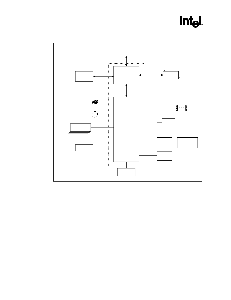
This chapter provides a detailed description of the MCH signals. The signal descriptions are
arranged in functional groups according to their associated interface (see Figure 1). The states of
all of the signals during reset are provided in the System Reset section.
The "#" symbol at the end of a signal name indicates that the active, or asserted state occurs when
the signal is at a low voltage level. When "#" is not present after the signal name the signal is
asserted when at the high voltage level.
The following notations are used to describe the signal type:
I Input
pin
O Output
pin
I/O
Bi-directional Input/Output pin
s/t/s
Sustained Three-state. This pin is driven to its inactive state prior to three-
stating.
as/t/s
Active Sustained Three-state. This applies to some of the hub interface signals.
This pin is weakly driven to its last driven value.
The signal description also includes the type of buffer used for the particular signal:
AGTL+
Open Drain AGTL+ interface signal. Refer to the AGTL+ I/O Specification for
complete details. The MCH integrates AGTL+ termination resistors.
AGP
AGP interface signals. These signals are compatible with AGP 2.0 1.5 V
Signaling Environment DC and AC Specifications. The buffers are not 3.3 V
tolerant.
CMOS
CMOS buffers.
Ref
Voltage reference signal
Note: System address and data bus signals are logically inverted signals. In other words, the actual
values are inverted of what appears on the system bus. This must be taken into account and the
addresses and data bus signals must be inverted inside the MCH. All processor control signals
follow normal convention. A "0" indicates an active level (low voltage) if the signal is followed by
"#" symbol, and a "1" indicates an active level (high voltage) if the signal has no "#" suffix.

Signal Description
R
20
Intel
ģ
82845 MCH Datasheet
Figure 1. Intel
ģ
82845 MCH Signal Interface Diagram
block_dia_845
SCS[3:0]#
SMA[12:0]
SBS[1:0]
SRAS#
SCAS#
SWE#
SDQ[63:0]
SCB[7:0]
SDQS[8:0]
SCKE[3:0]
RCVENOUT#
RCVENIN#
AGP
Interface
SBA[7:0]
PIPE#
ST[2:0]
RBF#
WBF#
AD_STB[1:0], AD_STB[1:0]#
SB_STB, SB_STB#
AGPRCOMP
G_FRAME#
G_IRDY#
G_TRDY#
G_STOP#
G_DEVSEL#
G_REQ#
G_GNT#
G_AD[31:0]
G_C/BE[3:0]#
G_PAR
Processor
System
Bus
Interface
HA[31:3]#
HD[63:0]#
ADS#
BNR#
BPRI#
DBSY#
DEFER#
DRDY#
HIT#
HITM#
HLOCK#
HREQ[4:0]#
HTRDY#
RS[2:0]#
CPURST#
BR0#
DBI[3:0]#
HADSTB[1:0]#
HDSTBP[3:0]#/HDSTBN[3:0]#
System
Memory
SDRAM
Interface
Hub
Interface
HI_[10:0]
HI_STB, HI_STB#
HVREF
SDREF
HI_REF
AGPREF
HLRCOMP
GRCOMP
HRCOMP[1:0]
HSWNG[1:0]
SMRCOMP
VCC1_5
VCC1_8
VCCSM
VCCA[1:0]
VTT
VSS
VSSA[1:0]
Voltage
Refernce,
PLL Power
BCLK, BCLK#
66IN
SCK[5:0], SCK[5:0]#
RSTIN#
TESTIN#
Clocks
and
Reset

Signal Description
R
Intel
ģ
82845 MCH Datasheet 21
2.1
System Bus Signals
Signal Name
Type
Description
ADS# I/O
AGTL+
Address Strobe: The system bus owner asserts ADS# to indicate the first
of two cycles of a request phase.
BNR# I/O
AGTL+
Block Next Request: BNR# is used to block the current request bus
owner from issuing a new request. This signal dynamically controls the
system bus pipeline depth.
BPRI# O
AGTL+
Bus Priority Request: The MCH is the only Priority Agent on the system
bus. It asserts this signal to obtain the ownership of the address bus. This
signal has priority over symmetric bus requests and will cause the current
symmetric owner to stop issuing new transactions unless the HLOCK#
signal was asserted.
BR0# I/O
AGTL+
Bus Request 0#: The MCH pulls the processor bus BR0# signal low
during CPURST#. The signal is sampled by the processor on the active-to-
inactive transition of CPURST#. The minimum setup time for this signal is
4 BCLKs. The minimum hold time is 2 BCLKs and the maximum hold time
is 20 BCLKs. BR0# should be three-stated after the hold time requirement
has been satisfied.
CPURST# O
AGTL+
Processor Reset: The CPURST# pin is an output from the MCH. The
MCH asserts CPURST# while RSTIN# (PCIRST# from the ICH4) is
asserted and for approximately 1 ms after RSTIN# is deasserted. The
CPURST# allows the processor to begin execution in a known state.
DBSY# I/O
AGTL+
Data Bus Busy: DBSY# is used by the data bus owner to hold the data
bus for transfers requiring more than one cycle.
DEFER# O
AGTL+
Defer Response: This signal, when asserted, indicates that the MCH will
terminate the transaction currently being snooped with either a deferred
response or with a retry response.
DBI[3:0]# I/O
AGTL+
Dynamic Bus Inversion: DBI[3:0]# are driven along with the HD[63:0]#
signals. DBI[3:0]# Indicate if the associated data signals are inverted.
DBI[3:0]# are asserted such that the number of data bits driven electrically
low (low voltage) within the corresponding 16-bit group never exceeds 8.
DBI[x]# Data
Bits
DBI3# HD[63:48]#
DBI2# HD[47:32]#
DBI1# HD[31:16]#
DBI0# HD[15:0]#
DRDY# I/O
AGTL+
Data Ready: Asserted for each cycle that data is transferred.
HA[31:3]# I/O
AGTL+
Host Address Bus: HA[31:3]# connect to the system address bus. During
processor cycles, HA[31:3]# are inputs. The MCH drives HA[31:3]# during
snoop cycles on behalf of the hub interface and AGP/Secondary PCI
initiators. HA[31:3]# are transferred at 2X rate. Note that the address is
inverted on the system bus.
HADSTB[1:0]# I/O
AGTL+
Host Address Strobe: The source synchronous strobes used to transfer
HA[31:3]# and HREQ[4:0]# at the 2X transfer rate.
Strobe Address
Bits
HADSTB0#
HA[16:3]#, HREQ[4:0]#
HADSTB1#
HA[31:17]#

Signal Description
R
22
Intel
ģ
82845 MCH Datasheet
Signal Name
Type
Description
HD[63:0]# I/O
AGTL+
Host Data: These signals are connected to the system data bus.
HD[63:0]# are transferred at a 4X rate. Note that the data signals are
inverted on the system bus.
HDSTBP[3:0]#
HDSTBN[3:0]#
I/O
AGTL+
Differential Host Data Strobes: The differential source synchronous
strobes used to transfer HD[63:0]# and DBI[3:0]# at the 4X transfer rate.
Strobe Data
Bits
HDSTBP3#, HDSTBN3#
HD[63:48]#, DBI3#
HDSTBP2#, HDSTBN2#
HD[47:32]#, DBI2#
HDSTBP1#, HDSTBN1#
HD[31:16]#, DBI1#
HDSTBP0#, HDSTBN0#
HD[15:0]#, DBI0#
HIT# I/O
AGTL+
Hit: This signal indicates that a caching agent holds an unmodified version
of the requested line. HIT# is also driven in conjunction with HITM# by the
target to extend the snoop window.
HITM# I/O
AGTL+
Hit Modified: This signal indicates that a caching agent holds a modified
version of the requested line and that this agent assumes responsibility for
providing the line. HITM# is also driven in conjunction with HIT# to extend
the snoop window.
HLOCK# I
AGTL+
Host Lock: All system bus cycles sampled with the assertion of HLOCK#
and ADS#, until the negation of HLOCK# must be atomic (i.e., no hub
interface or AGP snoopable access to system memory are allowed when
HLOCK# is asserted by the processor).
HREQ[4:0]# I/O
AGTL+
Host Request Command: These signals define the attributes of the
request. In Enhanced Mode HREQ[4:0]# are transferred at 2X rate.
HREQ[4:0]# are asserted by the requesting agent during both halves of
Request Phase. In the first half the signals define the transaction type to a
level of detail that is sufficient to begin a snoop request. In the second half
the signals carry additional information to define the complete transaction
type.
The transactions supported by the MCH host bridge are defined in the
Section 5.1.
HTRDY# O
AGTL+
Host Target Ready: HTRDY# indicates that the target of the processor
transaction is able to enter the data transfer phase.
RS[2:0]# O
AGTL+
Response Status: RS[2:0]# indicates the type of response according to
the following the table:
RS[2:0] Response
Type
000
Idle
state
001
Retry
response
010
Deferred
response
011
Reserved (not driven by MCH)
100
Hard Failure (not driven by MCH)
101
No data response
110
Implicit
Write
back
111
Normal
data
response
Signal Description
R
Intel
ģ
82845 MCH Datasheet 23
2.2
DDR SDRAM Interface Signals
Signal Name
Type
Description
SCS[3:0]# O
CMOS
Chip Select: These signals select the particular SDRAM components
during the active state.
Note: There is one SCS# signal per SDRAM row. This signal can be
toggled on every rising SCKx clock edge.
SMA[12:0] O
CMOS
Multiplexed Memory Address: These signals are used to provide the
multiplexed row and column address to SDRAM.
SBS[1:0] O
CMOS
Memory Bank Select: SBS[1:0] define the banks that are selected within
each SDRAM row. The SMA and SBS signals combine to address every
possible location in a SDRAM device.
SRAS# O
CMOS
SDRAM Row Address Strobe: SRAS# is Used with SCAS# and SWE#
(along with SCS#) to define the DRAM commands.
SCAS# O
CMOS
SDRAM Column Address Strobe: SCAS# is used with SRAS# and
SWE# (along with SCS#) to define the SDRAM commands.
SWE# O
CMOS
Write Enable: SWE# is used with SCAS# and SRAS# (along with SCS#)
to define the SDRAM commands.
SDQ[63:0] I/O
CMOS
Data Lines: These signals are used to interface to the SDRAM data bus.
SCB[7:0] I/O
CMOS
Check Bit Data Lines: These signals are used to interface to the
SDRAM ECC signals.
SDQS[8:0] I/O
CMOS
Data Strobes: The following list indicates the data byte and strobe
signal association:
Signal Data
Byte
SDQS8
SCB[7:0]
SDQS7
SDQ[63:56]
SDQS6
SDQ[55:48]
SDQS5
SDQ[47:40]
SDQS4
SDQ[39:32]
SDQS3
SDQ[31:24]
SDQS2
SDQ[23:16]
SDQS1
SDQ[15:8]
SDQS0
SDQ[7:0]
SCKE[3:0] O
CMOS
Clock Enable: These pins are used to signal a self-refresh or
Powerdown command to a SDRAM array when entering system
suspend. There is one SCKE per SDRAM row. These signals can be
toggled on every rising SCKx edge.
RCVENOUT# O
CMOS
Clock Output: RCVENOUT# is Part of the feedback used to enable the
DQS input buffers during reads. This signal Connects to RCVENIN#.
RCVENIN# I
CMOS
Clock Input: RCVENIN# connects to RCVENOUT#. This input (driven
from RCVENOUT#) enables the DQS input buffers during reads.

Signal Description
R
24
Intel
ģ
82845 MCH Datasheet
2.3
Hub Interface Signals
Signal Name
Type
Description
HI_[10:0] I/O
CMOS
Hub Interface Signals: Signals used for the hub interface.
HI_STB I/O
CMOS
Hub Interface Strobe: One of two differential strobe signals used to
transmit or receive packet data over the hub interface.
HI_STB# I/O
CMOS
Hub Interface Strobe Compliment: One of two differential strobe
signals used to transmit or receive packet data over the hub interface.
2.4
AGP Interface Signals
2.4.1
AGP Addressing Signals
Signal Name
Type
Description
PIPE# I
AGP
Pipelined Read: This signal is asserted by the AGP master to indicate a
full-width address is to be enqueued on by the target using the AD bus.
One address is placed in the AGP request queue on each rising clock
edge while PIPE# is asserted. When PIPE# is deasserted, no new
requests are queued across the AD bus.
During SBA Operation: Not Used.
During FRAME# Operation: Not Used.
PIPE# is a sustained three-state signal from masters (graphics
controller), and is an MCH input.
Note: Initial AGP designs may not use PIPE# (i.e., PCI only 66 MHz).
Therefore, an 8 k
pull-up resistor connected to this pin is
required on the motherboard.
SBA[7:0] I
AGP
Sideband Address: These signals are used by the AGP master
(graphics controller) to place addresses into the AGP request queue.
The SBA bus and AD bus operate independently. That is, a transaction
can proceed on the SBA bus and the AD bus simultaneously.
During PIPE# Operation: Not Used.
During FRAME# Operation: Not Used.
Note: When sideband addressing is disabled, these signals are
isolated (no external/internal pull-up resistors are required).
NOTE: The above table contains two mechanisms to queue requests by the AGP master. Note that the
master can only use one mechanism. The master may not switch methods without a full reset of the
system. When PIPE# is used to queue addresses the master is not allowed to queue addresses using
the SBA bus. For example, during configuration time, if the master indicates that it can use either
mechanism, the configuration software will indicate which mechanism the master will use. Once this
choice has been made, the master will continue to use the mechanism selected until the master is
reset (and reprogrammed) to use the other mode. This change of modes is not a dynamic mechanism
but rather a static decision when the device is first being configured after reset.

Signal Description
R
Intel
ģ
82845 MCH Datasheet 25
2.4.2
AGP Flow Control Signals
Signal Name
Type
Description
RBF# I
AGP
Read Buffer Full: RBF# indicates if the master is ready to accept
previously requested low priority read data. When RBF# is asserted, the
MCH is not allowed to initiate the return low priority read data. That is, the
MCH can finish returning the data for the request currently being
serviced. RBF# is only sampled at the beginning of a cycle. If the AGP
master is always ready to accept return read data, then it is not required
to implement this signal.
During FRAME# Operation: Not Used.
WBF# I
AGP
Write-Buffer Full: Indicates if the master is ready to accept fast write
data from the MCH. When WBF# is asserted, the MCH is not allowed to
drive fast write data to the AGP master. WBF# is only sampled at the
beginning of a cycle. If the AGP master is always ready to accept fast
write data, then it is not required to implement this signal.
During FRAME# Operation: Not Used.
2.4.3
AGP Status Signals
Signal Name
Type
Description
ST[2:0] O
AGP
Status: ST[2:0] provides information from the arbiter to an AGP Master
on what it may do. ST[2:0] only have meaning to the master when its
G_GNT# is asserted. When G_GNT# is deasserted, these signals have
no meaning and must be ignored. Refer to the AGP Interface
Specification, Revision 2.0 for further explanation of the ST[2:0] values
and their meanings.
During FRAME# Operation: These signals are not used during
FRAME#-based operation, except that a `111' indicates that the master
may begin a FRAME# transaction.

Signal Description
R
26
Intel
ģ
82845 MCH Datasheet
2.4.4
AGP Strobes Signals
Signal Name
Type
Description
AD_STB0 I/O
(s/t/s)
AGP
Address/Data Bus Strobe-0: This signal provides timing for 2X and 4X
data on AD[15:0] and the C/BE[1:0]# signals. The agent that is providing
the data drives this signal.
AD_STB0# I/O
(s/t/s)
AGP
Address/Data Bus Strobe-0 Compliment: Differential strobe pair that
provides timing information for the AD[15:0] and C/BE[1:0]# signals. The
agent that is providing the data drives this signal.
AD_STB1 I/O
(s/t/s)
AGP
Address/Data Bus Strobe-1: This signal provides timing for 2X- and 4X-
clocked data on AD[31:16] and C/BE[3:2]# signals. The agent that is
providing the data drives this signal.
AD_STB1# I/O
(s/t/s)
AGP
Address/Data Bus Strobe-1 Compliment: The differential compliment
to the AD_STB1 signal. It is used to provide timing for 4X-clocked data.
SB_STB I
AGP
Sideband Strobe: This signal provides timing for 2X- and 4X- clocked
data on the SBA[7:0] bus. It is driven by the AGP master after the system
has been configured for 2X- or 4X- clocked sideband address delivery.
SB_STB# I
AGP
Sideband Strobe Compliment: SB_STB# is the differential compliment
to the SB_STB signal. It is used to provide timing for 4X-clocked data.
2.4.5 AGP/PCI
Signals
For transactions on the AGP interface carried using AGP FRAME# protocol, these signals operate
similar to their semantics in the PCI 2.1 specification the exact role of all AGP FRAME# signals
are defined below.
Signal Name
Type
Description
G_FRAME# I/O
s/t/s
AGP
FRAME: During FRAME# Operations, G_FRAME# is an output when the
MCH acts as an initiator on the AGP Interface.
G_IRDY# I/O
s/t/s
AGP
Initiator Ready#: This signal indicates the AGP compliant master is
ready to provide all write data for the current transaction. Once G_IRDY#
is asserted for a write operation, the master is not allowed to insert wait-
states. The master is never allowed to insert a wait-state during the initial
data transfer (32 bytes) of a write transaction. However, it may insert
wait-states after each 32-byte block is transferred.
G_TRDY# I/O
s/t/s
AGP
Target Ready: This signal indicates the AGP compliant target is ready to
provide read data for the entire transaction (when the transfer size is less
than or equal to 32 bytes) or is ready to transfer the initial or subsequent
block (32 bytes) of data when the transfer size is greater than 32 bytes.
The target is allowed to insert wait-states after each block (32 bytes) is
transferred on write transactions.
G_STOP# I/O
s/t/s
AGP
STOP: G_STOP Is an input when the MCH acts as a FRAME#-based
AGP initiator and an output when the MCH acts as a FRAME#-based
AGP target. G_STOP# is used for disconnect, retry, and abort
sequences on the AGP interface.

Signal Description
R
Intel
ģ
82845 MCH Datasheet 27
Signal Name
Type
Description
G_DEVSEL# I/O
s/t/s
AGP
Device Select: This signal indicates that a FRAME#-based AGP target
device has decoded its address as the target of the current access. The
MCH asserts G_DEVSEL# based on the DRAM address range being
accessed by a PCI initiator. As an input it indicates whether any device
on the bus has been selected.
G_REQ# I
AGP
Request: Indicates that a FRAME# or PIPE#-based AGP master is
requesting use of the AGP interface. This signal is an input into the
MCH.
G_GNT# O
AGP
Grant: During SBA, PIPE# and FRAME# operation, G_GNT#, along with
the information on the ST[2:0] signals (status bus), indicates how the
AGP interface will be used next.
G_AD[31:0] I/O
AGP
Address/Data Bus: These signals are used to transfer both address and
data on the AGP interface.
G_C/BE[3:0]# I/O
AGP
Command/Byte Enable:
During FRAME# Operation: During the address phase of a transaction,
G_C/BE[3:0]# define the bus command. During the data phase,
G_C/BE[3:0]# are used as byte enables. The byte enables determine
which byte lanes carry meaningful data.
During PIPE# Operation: When an address is enqueued using PIPE#,
the G_C/BE# signals carry command information. The command
encoding used during PIPE#-based AGP is DIFFERENT than the
command encoding used during FRAME#-based AGP cycles (or
standard PCI cycles on a PCI bus).
G_PAR I/O
AGP
Parity:
During FRAME# Operations: This signal is driven by the MCH when it
acts as a FRAME#-based AGP initiator during address and data phases
for a write cycle, and during the address phase for a read cycle. PAR is
driven by the MCH when it acts as a FRAME#-based AGP target during
each data phase of a FRAME#-based AGP memory read cycle. Even
parity is generated across AD[31:0] and G_C/BE[3:0]#.
During SBA and PIPE# Operation: This signal is not used during SBA
and PIPE# operation.
NOTE: PCIRST# from the ICH4 is connected to RSTIN# and is used to reset AGP interface logic within the
MCH. The AGP agent will also use PCIRST# provided by the ICH4 as an input to reset its internal
logic.

Signal Description
R
28
Intel
ģ
82845 MCH Datasheet
2.5
Clocks, Reset, and Miscellaneous Signals
Signal Name
Type
Description
BCLK
BCLK#
I
CMOS
Differential Host Clock In: These pins receive a differential host clock
from the external clock synthesizer. This clock is used by all of the MCH
logic that is in the host clock domain.
66IN I
CMOS
66 MHz Clock In: This pin receives a 66-MHz clock from the clock
synthesizer. This clock is used by AGP/PCI and hub interface clock
domains.
Note: That this clock input is 3.3 V tolerant.
SCK[5:0] O
CMOS
SDRAM Differential Clock (DDR): These signals deliver a source
synchronous clock to the DIMMs. There are three clocks per DIMM.
SCK[5:0]# O
CMOS
SDRAM Inverted Differential Clock (DDR): These signals are the
complement to the SCK[5:0] signals. There are three clocks per DIMM.
RSTIN# I
CMOS
Reset In: When asserted, this signal asynchronously resets the MCH
logic. RSTIN# is connected to the PCIRST# output of the ICH4. All
AGP/PCI output and bi-directional signals will also three-state compliant
to PCI Rev 2.0 and 2.1 specifications.
Note: This input needs to be 3.3 V tolerant.
TESTIN# I
CMOS
Test Input: This pin is used for manufacturing and board level test
purposes.
Note: This signal has an internal pull-up resistor.

Signal Description
R
Intel
ģ
82845 MCH Datasheet 29
2.6
Voltage Reference and Power Signals
Signal Name
Type
Description
HVREF Ref
Host Reference Voltage: Reference voltage input for the data, address,
and common clock signals of the host AGTL+ interface.
SDREF Ref
SDRAM Reference Voltage: Reference voltage input for DQ, DQS,
RCVENIN# (DDR).
HI_REF Ref
Hub Interface Reference: Reference voltage input for the hub interface.
AGPREF Ref
AGP Reference: Reference voltage input for the AGP interface.
HLRCOMP I/O
CMOS
Compensation for Hub Interface: This signal is used to calibrate the
hub interface I/O buffers. It is connected to a 40.2
pull-up resistor with
1% tolerance and is pulled up to VCC1_8.
GRCOMP I/O
CMOS
Compensation for AGP: This signal is used to calibrate buffers. It is
connected to a 40.2
pull-down resistor with a 1% tolerance.
HRCOMP[1:0] I/O
CMOS
Compensation for Host: These signals are used to calibrate the host
AGTL+ I/O buffers. Each signal is connected to a 24.9
pull-down
resistor with a 1% tolerance.
HSWNG[1:0] I
CMOS
Host Reference Voltage: Reference voltage input for the compensation
logic.
SMRCOMP I/O
CMOS
System Memory RCOMP: This signal is used to calibrate the system
memory buffers.
VCC1_5
1.5 V Power Input: These pins are connected to a 1.5 V power source.
VCC1_8
1.8 V Power Input Pins: These pins are connected to a 1.8 V power
source.
VCCSM
SDRAM Power Input Pins: These pins are connected to a 2.5 V power
source for DDR.
VCCA[1:0]
PLL Power Input Pins: These pins provide power for the PLL.
VTT
AGTL+ Bus Termination Voltage Inputs: These pins provide the
AGTL+ bus termination.
VSS
Ground: The VSS pins are the ground pins for the MCH.
VSSA[1:0]
PLL
Ground:
The VSSA[1:0] pins are the ground pins for the PLL on
the MCH.
Signal Description
R
30
Intel
ģ
82845 MCH Datasheet
2.7
Pin States during Reset
Z Ti-state
ISO
Isolate inputs in inactive state
S
Strap input sampled during assertion or on the de-asserting edge of RSTIN#
H Driven
high
L Driven
low
D
Strong drive (to normal value supplied by core logic if not otherwise stated)
I Input
active
Signal Name
State
During
RSTIN#
Assertion
System Bus Interface
CPURST# L
HADSTB[1:0]# Z/I
AP[1:0]# Z/I
HA[31:4]# Z/I
HD[63:0]# Z/I
HDSTBP[3:0]# Z/I
HDSTBN[3:0]# Z/I
DBI[3:0]# Z/I
ADS# Z/I
BNR# Z/I
BPRI# Z/I
DBSY# Z/I
DEFER# Z/I
DRDY# Z/I
HIT# Z/I
HITM# Z/I
HLOCK# Z/I
HREQ[4:0]# Z/I
HTRDY# Z/I
RS[2:0]# Z/I
BREQ0# Z/I
HVREF I
HLRCOMP Z
Signal Name
State
During
RSTIN#
Assertion
HSWNG I
DDR System Memory
SCK[5:0] Z
SCS[3:0]# Z
SMA[12:0] Z
SBS[1:0] Z
SRAS# Z
SCAS# Z
SWE# Z
SDQ[63:0] Z/I
SCB[7:0] Z
SDQS[8:0] Z
SCKE[3:0] L
RCVENOUT# Z
RCVENIN# I
AGP
PIPE# I
SBA[7:0] ISO/S
RBF# I
WBF# I/S
G_REQ# I
ST[2:0] L/S
G_GNT# H/S
AD_STB[1:0] Z
Signal Name
State
During
RSTIN#
Assertion
AD_STB[1:0]# Z
SB_STB I
SB_STB# I
G_AD[31:0] Z
G_C/BE[3:0]# Z
G_FRAME# Z/I
G_IRDY# Z/I
G_TRDY# Z/I
G_STOP# Z/I
G_DEVSEL# Z/I
G_PAR Z
AGPREF Z
Hub Interface
HI_[10:0] Z/I
HI_STB Z/I
HI_STB# Z/I
Clocks
BCLK I
Miscellaneous
RSTIN# I
TESTIN# I

Register Description
R
Intel
ģ
82845 MCH Datasheet 31
3 Register
Description
The MCH contains two sets of software accessible registers, accessed via the host processor I/O
address space:
∑
Control registers I/O mapped into the processor I/O space, which control access to PCI and
AGP configuration space (see Section 3.3).
∑
Internal configuration registers residing within the MCH are partitioned into two logical
device register sets ("logical" since they reside within a single physical device). The first
register set is for Host-to-Hub Interface bridge and other functionality (i.e., DRAM
configuration, other chipset operating parameters, and optional features). The second register
set is dedicated to Host-to-AGP Bridge functions (controls AGP interface configurations and
operating parameters).
The MCH supports PCI configuration space accesses using the mechanism denoted as
Configuration Mechanism #1 in the PCI specification.
The MCH internal registers (I/O Mapped and configuration registers) are accessible by the
processor. The registers can be accessed as Byte, Word (16-bit), or DWord (32-bit) quantities,
with the exception of CONF_ADDR which can only be accessed as a DWord. All multi-byte
numeric fields use "little-endian" ordering (i.e., lower addresses contain the least significant parts
of the field).
3.1 Register
Terminology
Term Description
RO
Read Only. If a register is read only, writes to this register have no effect.
R/W
Read/Write. A register with this attribute can be read and written.
R/W/L
Read/Write/Lock. A register with this attribute can be read, written, and locked.
R/WC
Read/Write Clear. A register bit with this attribute can be read and written. However, a
write of a 1 clears (sets to 0) the corresponding bit and a write of a 0 has no effect.
R/WO
Read/Write Once. A register bit with this attribute can be written to only once after
power up. After the first write, the bit becomes read only.
L
Lock. A register bit with this attribute becomes Read Only after a lock-bit is set.
Reserved Bits
Some of the MCH registers described in this section contain reserved bits. These bits
are labeled "Reserved". Software must deal correctly with fields that are reserved. On
reads, software must use appropriate masks to extract the defined bits and not rely on
reserved bits being any particular value. On writes, software must ensure that the
values of reserved bit positions are preserved. That is, the values of reserved bit
positions must first be read, merged with the new values for other bit positions and
then written back. Note that software does not need to perform a read-merge-write
operation for the Configuration Address (CONF_ADDR) register.
Register Description
R
32
Intel
ģ
82845 MCH Datasheet
Term Description
Reserved
Registers
In addition to reserved bits within a register, the MCH contains address locations in the
configuration space that are marked "Reserved". When a "Reserved" register location
is read, a random value is returned. ("Reserved" registers can be 8-, 16-, or 32-bits in
size). Registers that are marked as "Reserved" must not be modified by system
software. Writes to "Reserved" registers may cause system failure.
Default Value
upon a Reset
Upon a Full Reset, the MCH sets all of its internal configuration registers to
predetermined default states. Some register values at reset are determined by
external strapping options. The default state represents the minimum functionality
feature set required to successfully bring up the system. Hence, it does not represent
the optimal system configuration. It is the responsibility of the system initialization
software (usually BIOS) to properly determine the DRAM configurations, operating
parameters and optional system features that are applicable, and to program the MCH
registers accordingly.
3.2
PCI Bus Configuration Space Access
The MCH and ICH4 are physically connected by the hub interface. From a configuration
standpoint, the hub interface is PCI bus 0. As a result, all devices internal to the MCH and ICH4
appear to be on PCI bus 0. The system's primary PCI expansion bus is physically attached to the
ICH4 and, from a configuration perspective appears to be a hierarchical PCI bus behind a PCI-PCI
bridge and, therefore, has a programmable PCI Bus number. Note that the primary PCI bus is
referred to as PCI_A in this document and is not PCI bus #0 from a configuration
standpoint. The AGP appears to system software to be a real PCI bus behind PCI-PCI bridges
resident as devices on PCI bus 0.
The MCH contains two PCI devices within a single physical component. The configuration
registers for the four devices are mapped as devices residing on PCI bus 0.
∑
Device 0: Host-to-Hub Interface Bridge/DRAM Controller. Logically this appears as a PCI
device residing on PCI bus 0. Physically, Device 0 contains the standard PCI registers,
DRAM registers, the Graphics Aperture controller, and other MCH specific registers.
∑
Device 1: Host-to-AGP Bridge. Logically this appears as a "virtual" PCI-PCI bridge residing
on PCI bus 0. Physically Device 1 contains the standard PCI-to-PCI bridge registers and the
standard AGP/PCI configuration registers (including the AGP I/O and memory address
mapping).
Table 6 shows the Device # assignment for the various internal MCH devices.
Table 6. MCH Internal Device Assignments
MCH Function
Bus 0, Device #
DRAM Controller/8 bit HI_A Controller
Device 0
Host-to-AGP Bridge (virtual PCI-to-PCI)
Device 1
NOTE: A physical PCI bus 0 does not exist. The hub interface and the internal devices in
the MCH and ICH4, logically constitute PCI Bus 0 to configuration software.

Register Description
R
Intel
ģ
82845 MCH Datasheet 33
3.2.1
Standard PCI Bus Configuration Mechanism
The PCI Bus defines a slot based "configuration space" that allows each device to contain up to
eight functions with each function containing up to 256 8-bit configuration registers. The PCI
specification defines two bus cycles to access the PCI configuration space: Configuration Read
and Configuration Write. Memory and I/O spaces are supported directly by the processor.
Configuration space is supported by a mapping mechanism implemented within the MCH. The
PCI specification defines two mechanisms to access configuration space, Mechanism #1 and
Mechanism #2. The MCH supports only Mechanism #1.
The configuration access mechanism makes use of the CONF_ADDR Register (at I/O address
0CF8h though 0CFBh) and CONF_DATA register (at I/O address 0CFCh though 0CFFh). To
reference a configuration register a DWord I/O write cycle is used to place a value into
CONF_ADDR that specifies the PCI bus, the device on that bus, the function within the device,
and a specific configuration register of the device function being accessed. CONF_ADDR[31]
must be 1 to enable a configuration cycle. CONF_DATA then becomes a window into the four
bytes of configuration space specified by the contents of CONF_ADDR. Any read or write to
CONF_DATA results in the MCH translating the CONF_ADDR into the appropriate
configuration cycle.
The MCH is responsible for translating and routing the processor's I/O accesses to the
CONF_ADDR and CONF_DATA registers to internal MCH configuration registers, hub interface
or AGP.
3.2.2
Routing Configuration Accesses
The MCH supports two bus interfaces: the hub interface and AGP. PCI configuration cycles are
selectively routed to one of these interfaces. The MCH is responsible for routing PCI configuration
cycles to the proper interface. PCI configuration cycles to the ICH4 internal devices and Primary
PCI (including downstream devices) are routed to the ICH4 via the hub interface. AGP
configuration cycles are routed to AGP. The AGP interface is treated as a separate PCI bus from
the configuration point of view. Routing of configuration AGP is controlled via the standard PCI-
to-PCI bridge mechanism using information contained within the Primary Bus Number, the
Secondary Bus Number, and the Subordinate Bus Number registers of the corresponding PCI-to-
PCI bridge device.
A detailed description of the mechanism for translating processor I/O bus cycles to configuration
cycles on one of the buses is described below.
PCI Bus 0 Configuration Mechanism
The MCH decodes the Bus Number (bits 23:16) and the Device Number fields of the
CONF_ADDR register. If the Bus Number field of CONF_ADDR is 0, the configuration cycle is
targeting a PCI Bus 0 device.
∑
The Host-HI Bridge entity in the MCH is hardwired as Device 0 on PCI Bus 0.
∑
The Host-AGP Bridge entity in the MCH is hardwired as Device 1 on PCI Bus 0.
Configuration cycles to any of the MCH's internal devices are confined to the MCH and not sent
over the hub interface. Accesses to disabled MCH internal devices are forwarded over the hub
interface as Type 0 Configuration Cycles.

Register Description
R
34
Intel
ģ
82845 MCH Datasheet
Primary PCI and Downstream Configuration Mechanism
If the Bus Number in the CONF_ADDR is non-zero, and is less than the value in the Host-AGP
device's Secondary Bus Number register, or greater than the value in the Host-AGP device's
Subordinate Bus Number register, the MCH will generate a Type 1 hub interface configuration
cycle. The ICH4 compares the non-zero Bus Number with the Secondary Bus Number and
Subordinate Bus Number registers of its PCI-to-PCI bridges to determine if the configuration
cycle is meant for Primary PCI, or a downstream PCI bus.
AGP Configuration Mechanism
From the chip-set configuration perspective, AGP is seen as a PCI bus interface residing on a
Secondary Bus side of the "virtual" PCI-to-PCI bridges referred to as the MCH Host-AGP bridge.
On the Primary Bus side, the "virtual" PCI-to-PCI bridge is attached to PCI Bus 0. Therefore, the
Primary Bus Number register is hardwired to 0. The "virtual" PCI-to-PCI bridge entity converts
Type 1 PCI bus configuration cycles on PCI Bus 0 into Type 0 or Type 1 configuration cycles on
the AGP interface. Type 1 configuration cycles on PCI Bus 0 that have a Bus Number that
matches the Secondary Bus Number of the MCH's "virtual" Host-to-PCI_B/AGP bridge will be
translated into Type 0 configuration cycles on the AGP interface.
If the Bus Number is non-zero, greater than the value programmed into the Secondary Bus
Number Register, and less than or equal to the value programmed into the Subordinate Bus
Number Register, the MCH will generate a Type 1 PCI configuration cycle on AGP.
3.3
I/O Mapped Registers
The MCH contains two registers that reside in the processor I/O address space: the Configuration
Address (CONF_ADDR) register and the Configuration Data (CONF_DATA) register. The
Configuration Address register enables/disables the configuration space and determines what
portion of configuration space is visible through the configuration data window.
3.3.1
CONF_ADDR--Configuration Address Register
I/O Address:
0CF8h Accessed as a DWord
Default Value:
00000000h
Access: R/W
Size: 32
bits
CONF_ADDR is a 32-bit register that can be accessed only as a DWord. A Byte or Word
reference will "pass through" the Configuration Address register and the hub interface, onto the
PCI bus as an I/O cycle. The CONF_ADDR register contains the Bus Number, Device Number,
Function Number, and Register Number for which a subsequent configuration access is intended.

Register Description
R
Intel
ģ
82845 MCH Datasheet 35
Bit Descriptions
31
Configuration Enable (CFGE).
0 = Disable.
1 = Enable. Accesses to PCI configuration space are enabled.
30:24
Reserved. These bits are read only and have a value of 0.
23:16
Bus Number. When Bus Number is programmed to 00h, the target of the configuration cycle is
a hub interface agent (MCH, ICH4, etc.).
The configuration cycle is forwarded to the hub interface, if Bus Number is programmed to 00h
and the MCH is not the target (the device number is
2).
If Bus Number is non-zero and matches the value programmed into the Secondary Bus Number
Register of device 1, a Type 0 PCI configuration cycle will be generated on AGP.
If Bus Number is non-zero, greater than the value in the Secondary Bus Number register of
device 1 and less than or equal to the value programmed into the Subordinate Bus Number
register of device 1 a Type 1 PCI configuration cycle will be generated on AGP.
If Bus Number is non-zero, and does not fall within the ranges enumerated by device 1's
Secondary Bus Number or Subordinate Bus Number register, then a hub interface Type 1
configuration cycle is generated.
15:11
Device Number. This field selects one agent on the PCI bus selected by the Bus Number field.
When the Bus Number field is 00, the MCH decodes the Device Number field. The MCH is
always Device Number 0 for the Host-Hub Interface bridge entity and Device Number 1 for the
Host-AGP entity. Therefore, when Bus Number =0 and Device Number=0≠1, the internal MCH
devices are selected.
If the Bus Number is non-zero and matches the value programmed into the Secondary Bus
Number register a Type 0 PCI configuration cycle is generated on AGP. The MCH decodes the
Device Number field ([15:11]) and assert the appropriate GAD signal as an IDSEL. For PCI-to-
PCI Bridge translation, one of the 16 IDSELs is generated. When bit [15] = 0, bits [14:11] are
decoded to assert a signal AD[31:16] IDSEL. GAD16 is asserted to access Device 0, GAD17 for
Device 1, and so forth up to Device 15 which asserts AD31. All device numbers higher than 15
cause a type 0 configuration access with no IDSEL asserted, which results in a Master Abort
reported in the MCH's "virtual" PCI-to-PCI bridge registers.
For Bus Numbers resulting in hub interface configuration cycles, the MCH propagates the device
number field as A[15:11]. For bus numbers resulting in AGP type 1 configuration cycles, the
device number is propagated as GAD[15:11].
10:8
Function Number. This field is mapped to GAD[10:8] during AGP configuration cycles and
A[10:8] during Hub Interface configuration cycles. This allows the configuration registers of a
particular function in a multi-function device to be accessed. The MCH ignores configuration
cycles to its internal devices if the function number is not equal to 0.
7:2
Register Number. This field selects one register within a particular bus, device, and function as
specified by the other fields in the Configuration Address register. This field is mapped to
GAD[7:2] during AGP configuration cycles and A[7:2] during hub interface configuration cycles.
1:0 Reserved.
Register Description
R
36
Intel
ģ
82845 MCH Datasheet
3.3.2
CONF_DATA--Configuration Data Register
I/O Address:
0CFCh
Default Value:
00000000h
Access: R/W
Size: 32
bits
CONF_DATA is a 32-bit read/write window into configuration space. The portion of
configuration space that is referenced by CONF_DATA is determined by the contents of
CONF_ADDR.
Bit Descriptions
31:0
Configuration Data Window (CDW). If bit 31 of the CONF_ADDR register is 1, any I/O access
to the CONF_DATA register will be mapped to configuration space using the contents of
CONF_ADDR.
3.4
Memory-Mapped Register Space
All system memory control functions have been consolidated into a new memory-mapped address
region within Device 0, Function 0. This space will be accessed using a new Base Address register
(BAR) located at Device 0, Function 0 (address offset 14h). By default this BAR is invisible
(i.e., read-only as 0s).
Note: All accesses to these memory-mapped registers must be made as a single DWord (4 bytes) or less.
Access must be aligned on a natural boundary.
The high-level address map for the memory-mapped registers is shown in Table 7.
Table 7. Memory-Mapped Register Address Map
Memory Address Offset
Register Group
020h≠02Bh Reserved
2Ch
DRAM Width Register
02Dh≠02Fh Reserved
030h≠034h Strength
Registers
040h≠0DFh Reserved
140h≠1DFh Reserved

Register Description
R
Intel
ģ
82845 MCH Datasheet 37
3.4.1
DRAMWIDTH--DRAM Width Register
Address Offset:
2Ch
Default Value:
00h
Access: R/W
Size: 8
bits
This register determines the width of SDRAM devices populated in each row of memory.
Bit Descriptions
7:4 Reserved.
3
Row 3 Width. Width of devices in Row 3
0 = 16-bit wide devices, or Unpopulated (default)
1 = 8-bit wide devices
2
Row 2 Width. Width of devices in Row 2
0 = 16-bit wide devices, or Unpopulated (default)
1 = 8-bit wide devices
1
Row 1 Width. Width of devices in Row 1
0 = 16-bit wide devices, or Unpopulated (default)
1 = 8-bit wide devices
0
Row 0 Width. Width of devices in Row 0
0 = 16-bit wide devices, or Unpopulated (default)
1 = 8-bit wide devices
Note: Since there are multiple clock signals assigned to each row of a DIMM, it is important to clarify
exactly which row width field affects which clock signal.
Row Parameters
DDR Clocks Affected
0 SCK[2:0]/SCK[2:0]#
1 SCK[2:0]/SCK[2:0]#
2 SCK[5:3]/SCK[5:3]#
3 SCK[5:3]/SCK[5:3]#

Register Description
R
38
Intel
ģ
82845 MCH Datasheet
3.4.2
DQCMDSTR--Strength Control Register (SDQ and CMD
Signal Groups)
Memory Address Offset:
30h
Default Value:
00h
Access: R/W
Size: 8
bits
This register controls the drive strength of the I/O buffers for the DQ/DQS and CMD signal
groups.
Bit Descriptions
7 Reserved.
6:4
CMD Strength Control (SRAS#, SCAS#, SWE#, SMA[12:0], SBS[1:0]). This field selects the
signal drive strength.
000 = 0.75 X (default)
001 = 1.00 X
010 = 1.25 X
011 = 1.50 X
100 = 2.00 X
101 = 2.50 X
110 = 3.00 X
111 = 4.00 X
3 Reserved.
2:0
SDQ/SDQS Strength Control. This field selects the signal drive strength.
000 = 0.75 X (default)
001 = 1.00 X
010 = 1.25 X
011 = 1.50 X
100 = 2.00 X
101 = 2.50 X
110 = 3.00 X
111 = 4.00 X

Register Description
R
Intel
ģ
82845 MCH Datasheet 39
3.4.3
CKESTR--Strength Control Register (SCKE Signal Group)
Memory Address Offset:
31h
Default Value:
00h
Access: R/W
Size: 8
bits
This register controls the drive strength of the I/O buffers for the CKE signal group. This group
has two possible loadings depending on the width of SDRAM devices used in each row of memory
(x8 or x16). The proper strength can be independently programmed for each configuration. The
actual strength used for each signal is determined by the DRAMWIDTH Register (offset 2Ch).
Bit Descriptions
7 Reserved.
6:4
SCKE x16 Strength Control. This field selects the signal drive strength.
000 = 0.75 X (default)
001 = 1.00 X
010 = 1.25 X
011 = 1.50 X
100 = 2.00 X
101 = 2.50 X
110 = 3.00 X
111 = 4.00 X
3 Reserved.
2:0
SCKE x8 Strength Control. This field selects the signal drive strength.
000 = 0.75 X (default)
001 = 1.00 X
010 = 1.25 X
011 = 1.50 X
100 = 2.00 X
101 = 2.50 X
110 = 3.00 X
111 = 4.00 X

Register Description
R
40
Intel
ģ
82845 MCH Datasheet
3.4.4
CSBSTR--Strength Control Register (SCS# Signal Group)
Memory Address Offset:
32h
Default Value:
00h
Access: R/W
Size: 8
bits
This register controls the drive strength of the I/O buffers for the SCS# signal group. This group
has two possible loadings depending on the width of SDRAM devices used in each row of memory
(x8 or x16). The proper strength can be independently programmed for each configuration. The
actual strength used for each signal is determined by the DRAMWIDTH Register (offset 2Ch).
Bit Descriptions
7 Reserved.
6:4
SCS# x16 Strength Control. This field selects the signal drive strength.
000 = 0.75 X (default)
001 = 1.00 X
010 = 1.25 X
011 = 1.50 X
100 = 2.00 X
101 = 2.50 X
110 = 3.00 X
111 = 4.00 X
3 Reserved.
2:0
SCS# x8 Strength Control. This field selects the signal drive strength.
000 = 0.75 X (default)
001 = 1.00 X
010 = 1.25 X
011 = 1.50 X
100 = 2.00 X
101 = 2.50 X
110 = 3.00 X
111 = 4.00 X

Register Description
R
Intel
ģ
82845 MCH Datasheet 41
3.4.5
CKSTR--Strength Control Register (Clock Signal Group)
Memory Address Offset:
33h
Default Value:
00h
Access: R/W
Size: 8
bits
This register controls the drive strength of the I/O buffers for the Clock (CK) signal group
including both the CK and CK# signals. This group has two possible loadings depending on the
width of SDRAM devices used in each row of memory (x8 or x16). The proper strength can be
independently programmed for each configuration. The actual strength used for each signal is
determined by the DRAMWIDTH Register (offset 2Ch).
Bit Descriptions
7 Reserved.
6:4
CK x16 Strength Control. This field selects the signal drive strength.
000 = 0.75 X (default)
001 = 1.00 X
010 = 1.25 X
011 = 1.50 X
100 = 2.00 X
101 = 2.50 X
110 = 3.00 X
111 = 4.00 X
3 Reserved.
2:0
CK x8 Strength Control. This field selects the signal drive strength.
000 = 0.75 X (default)
001 = 1.00 X
010 = 1.25 X
011 = 1.50 X
100 = 2.00 X
101 = 2.50 X
110 = 3.00 X
111 = 4.00 X

Register Description
R
42
Intel
ģ
82845 MCH Datasheet
3.4.6
RCVENSTR--Strength Control Register (RCVENOUT
Signal Group)
Memory Address Offset:
34h
Default Value:
00h
Access: R/W
Size: 8
bits
This register controls the drive strength of the I/O buffers for the Receive Enable Out signal group
(RDCLKO# signal).
Bit Descriptions
7:3 Reserved.
2:0
Receive Enable Out Signal Group (RCVEnOut) Strength Control. This field selects the
signal drive strength.
000 = 0.75 X (default)
001 = 1.00 X
010 = 1.25 X
011 = 1.50 X
100 = 2.00 X
101 = 2.50 X
110 = 3.00 X
111 = 4.00 X

Register Description
R
Intel
ģ
82845 MCH Datasheet 43
3.5
Host-to-Hub Interface Bridge/DRAM Controller
Registers (Device 0)
Table 8 provides the register address map for Device 0 PCI configuration space. An "s" in the
Default Value column indicates that a strap determines the power-up default value for that bit.
Table 8. Host-to-Hub Bridge/DRAM Controller Register Address Map (Device 0)
Address
Offset
Symbol Register
Name Default
Access
00≠01h VID
Vendor
Identification
8086h
RO
02≠03h DID
Device
Identification
1A30h
RO
04≠05h
PCICMD
PCI Command
0006h
RO, R/W
06≠07h
PCISTS
PCI Status
0090h
RO, R/WC
08h RID
Revision
Identification
11h
RO
09h --
Reserved.
--
--
0Ah SUBC
Sub-Class
Code
00h RO
0Bh
BCC
Base Class Code
06h
RO
0Dh MLT
Master
Latency
Timer
00h
RO
0Eh HDR
Header
Type
00h
RO
0Fh --
Reserved.
--
--
10≠13h
APBASE
Aperture Base Configuration
00000008h
RO, R/W
14≠2Bh --
Reserved.
-- --
2C≠2Dh
SVID
Subsystem Vendor Identification
0000h
R/WO
2E≠2Fh SID
Subsystem
Identification
0000h
R/WO
30≠33h --
Reserved.
-- --
34h CAPPTR
Capabilities
Pointer
A0h RO
35≠50h --
Reserved.
-- --
51h
AGPM
AGP Miscellaneous Configuration
00h
R/W
52≠5Fh --
Reserved.
-- --
60≠67h
DRB[0:7]
DRAM Row Boundary (8 registers)
00h
R/W
68≠6Fh --
Reserved.
-- --
70≠73h
DRA
DRAM Row Attribute (4 registers)
00h
R/W
74≠77h --
Reserved.
-- --
78≠7Bh
DRT
DRAM Timing Register
00000010h
R/W
7C≠7Fh
DRC
DRAM Controller Mode
0000h
R/W, RO
80≠85h --
Reserved.
-- --
86h DERRSYN
DRAM
Error
Syndrome
00h RO

Register Description
R
44
Intel
ģ
82845 MCH Datasheet
Address
Offset
Symbol Register
Name Default
Access
87≠8Bh --
Reserved.
-- --
8C≠8Fh
EAP
Error Address Pointer
00000000h
RO
90≠96h
PAM[0:6]
Programmable Attribute Map (7 Registers)
0000000000
0000h
RO, R/W
97h
FDHC
Fixed DRAM Hole Control
00h
R/W
98≠9Ch --
Reserved.
-- --
9Dh
SMRAM
System Management RAM Control
02h
RO, R/W,
R/W/L
9Eh
ESMRAMC
Extended System Mgmt RAM Control
38h
RO, R/W,
R/WC,
R/W/L
9Fh --
Reserved.
--
--
A0≠A3h ACAPID
AGP
Capability
Identifier
00200002h
RO
A4≠A7h AGPSTAT
AGP
Status
1F000216h RO
A8≠ABh AGPCMD AGP
Command
00000000h R/W
AC≠AFh -- Reserved.
-- --
B0≠B3h AGPCTRL
AGP
Control
00000000h R/W
B4h APSIZE
Aperture
Size
00h R/W
B5≠B7h --
Reserved
-- --
B8≠BBh
ATTBASE
Aperture Translation Table Base
00000000h
R/W
BCh
AMTT
AGP MTT Control
00h
R/W
BDh
LPTT
AGP Low Priority Transaction Timer
00h
R/W
BE≠C3h Reserved
C4≠C5h
TOM
Top of Low Memory
0000h
R/W
C6≠C7h
MCHCFG
MCH Configuration
0000h
R/W, RO
C8≠C9h ERRSTS Error
Status
0000h R/WC
CA≠CBh ERRCMD Error
Command
0000h R/W
CC≠CDh
SMICMD
SMI Command
0000h
R/W
CE≠CFh
SCICMD
SCI Command
0000h
R/W
D0≠DDh -- Reserved.
-- --
DE≠DFh SKPD Scratchpad
Data
0000h R/W
E0≠E3h --
Reserved.
-- --
E4≠E7h
CAPID
Product Specific Capability Identifier
F104A009h
RO
E8≠FFh --
Reserved.
-- --

Register Description
R
Intel
ģ
82845 MCH Datasheet 45
3.5.1
VID--Vendor Identification Register (Device 0)
Address Offset:
00≠01h
Default Value:
8086h
Attribute: RO
Size: 16
bits
The VID Register contains the vendor identification number. This 16-bit register combined with
the DID Register uniquely identifies any PCI device. Writes to this register have no effect.
Bit Description
15:0
Vendor Identification Number. This is a 16-bit value assigned to Intel.
Intel VID = 8086h.
3.5.2
DID--Device Identification Register (Device 0)
Address Offset:
02≠03h
Default Value:
1A30h
Attribute: RO
Size: 16
bits
This 16-bit register combined with the VID Register uniquely identifies any PCI device. Writes to
this register have no effect.
Bit Description
15:0
Device Identification Number. This is a 16-bit value assigned to the MCH Host-Hub Interface
Bridge Function #0.

Register Description
R
46
Intel
ģ
82845 MCH Datasheet
3.5.3
PCICMD--PCI Command Register (Device 0)
Address Offset:
04≠05h
Default: 0006h
Access: R/W,
RO
Size 16
bits
Since MCH Device 0 does not physically reside on PCI0, many of the bits are not implemented.
Bit Descriptions
15:10 Reserved.
9
Fast Back-to-Back--RO. Not implemented; Hardwired to 0. This bit controls whether or not the
master can do fast back-to-back write. Since device 0 is strictly a target this bit is not
implemented.
8
SERR Enable (SERRE)--R/W. This bit is a global enable bit for Device 0 SERR messaging.
The MCH does not have an SERR# signal. The MCH communicates the SERR# condition by
sending a SERR message to the ICH4.
0 = Disable. SERR message is not generated by the MCH for Device 0.
1 = Enable. The MCH is enabled to generate SERR messages over the hub interface for
specific Device 0 error conditions that are individually enabled in the ERRCMD Register. The
error status is reported in the ERRSTS and PCISTS registers.
NOTE: This bit only controls SERR message for the Device 0. Device 1 has its own SERRE
bits to control error reporting for error conditions occurring on their respective devices.
7
Address/Data Stepping--RO. Not implemented; Hardwired to 0.
6
Parity Error Enable (PERRE)--RO. Not implemented; Hardwired to 0.The PERR# signal is not
implemented by the MCH.
5
VGA Palette Snoop--RO. Not implemented; Hardwired to 0.
4
Memory Write and Invalidate Enable (MWIE)--RO. Not implemented; Hardwired to 0.
3
Special Cycle Enable (SCE)--RO. Not implemented; Hardwired to 0.
2
Bus Master Enable (BME)--RO. Hardwired to 1. The MCH is always enabled as a master on
the hub interface.
1
Memory Access Enable (MAE)--RO. Not implemented; Hardwired to 1. The MCH always
allows access to system memory.
0
I/O Access Enable (IOAE)--RO. Not implemented; Hardwired to 0.

Register Description
R
Intel
ģ
82845 MCH Datasheet 47
3.5.4
PCISTS--PCI Status Register (Device 0)
Address Offset:
06≠07h
Default Value:
0090h
Access: RO,
R/WC
Size: 16
bits
PCISTS is a 16-bit status register that reports the occurrence of error events on Device 0s on the
hub interface. Since MCH Device 0 is the Host-to-hub interface bridge, many of the bits are not
implemented.
Bit
Description
15 Reserved.
14
Signaled System Error (SSE)--R/WC.
0 = Software clears this bit by writing a 1 to it.
1 = MCH Device 0 generated an SERR message over the hub interface for any enabled Device
0 error condition. Device 0 error conditions are enabled in the PCICMD and ERRCMD
Registers. Device 0 error flags are read/reset from the PCISTS or ERRSTS Registers.
13
Received Master Abort Status (RMAS)--R/WC.
0 = Software clears this bit by writing a 1 to it.
1 = MCH generated a hub interface request that receives a Master Abort completion packet or
Master Abort Special Cycle.
12
Received Target Abort Status (RTAS)--R/WC.
0 = Software clears this bit by writing a 1 to it.
1 = MCH generated a hub interface request that receives a Target Abort completion packet or
Target Abort Special Cycle.
11
Signaled Target Abort Status (STAS)--RO. Not Implemented; Hardwired to 0. The MCH will
not generate a Target Abort hub interface completion packet or special cycle.
10:9
DEVSEL Timing (DEVT)--RO. Hardwired to 00. Hub interface does not comprehend
DEVSEL# protocol.
8
Master Data Parity Error Detected (DPD)--RO. Not Implemented; Hardwired to 0. PERR
signaling and messaging are not implemented by the MCH.
7
Fast Back-to-Back (FB2B)--RO. Hardwired to 1.
6:5 Reserved.
4
Capability List (CLIST)--RO.
1 = Indicates to the configuration software that this device/function implements a list of new
capabilities. A list of new capabilities is accessed via the CAPPTR Register (offset 34h).
CAPPTR contains an offset pointing to the start address within configuration space of this
device where the AGP Capability standard register resides.
3:0 Reserved.
Register Description
R
48
Intel
ģ
82845 MCH Datasheet
3.5.5
RID--Revision Identification Register (Device 0)
Address Offset:
08h
Default Value:
11h
Access: RO
Size: 8
bits
This register contains the revision number of the MCH Device 0. These bits are read only and
writes to this register have no effect.
Bit Description
7:0
Revision Identification Number. This is an 8-bit value that indicates the revision identification
number for the MCH Device 0.
E0 Stepping = 11h.
3.5.6
SUBC--Sub-Class Code Register (Device 0)
Address Offset:
0Ah
Default Value:
00h
Access: RO
Size: 8
bits
This register contains the Sub-Class Code for the MCH Device 0.
Bit Description
7:0
Sub-Class Code (SUBC). This is an 8-bit value that indicates the category of bridge of the
MCH.
00h = Host bridge.
3.5.7
BCC--Base Class Code Register (Device 0)
Address Offset:
0Bh
Default Value:
06h
Access: RO
Size: 8
bits
This register contains the Base Class Code of the MCH Device 0.
Bit Description
7:0
Base Class Code (BASEC). This is an 8-bit value that indicates the Base Class Code for the
MCH.
06h = Bridge device.

Register Description
R
Intel
ģ
82845 MCH Datasheet 49
3.5.8
MLT--Master Latency Timer Register (Device 0)
Address Offset:
0Dh
Default Value:
00h
Access: RO
Size: 8
bits
The hub interface does not comprehend the concept of Master Latency Timer. Therefore, this
register is not implemented.
Bit Description
7:0
Hardwired to 00h. Writes have no effect.
3.5.9
HDR--Header Type Register (Device 0)
Address Offset:
0Eh
Default: 00h
Access: RO
Size: 8
bits
This register identifies the header layout of the configuration space.
Bit Description
7:0
Hardwired to 00h. Writes have no effect.

Register Description
R
50
Intel
ģ
82845 MCH Datasheet
3.5.10
APBASE--Aperture Base Configuration Register (Device 0)
Address Offset:
10≠13h
Default: 0000_0008h
Access: R/W,
RO
Size: 32
bits
The APBASE is a standard PCI Base Address register that is used to set the base of the Graphics
Aperture. The standard PCI Configuration mechanism defines the base address configuration
register such that only a fixed amount of space can be requested (dependent on which bits are
hardwired to 0 or behave as hardwired to 0). To allow for flexibility (of the aperture), an
additional register called APSIZE is used as a "back-end" register to control, which bits of the
APBASE will behave as hardwired to 0. This register will be programmed by the MCH specific
BIOS code that runs before any of the generic configuration software is run.
Note: Bit 9 of the MCHCFG register is used to prevent accesses to the aperture range before this
register
is initialized by the configuration software and the appropriate translation table structure has been
established in the system memory.
Bit Description
31:28
Upper Programmable Base Address--R/W. These bits are part of the aperture base set by
configuration software to locate the base address of the graphics aperture. They correspond to
bits [31:28] of the base address in the processor's address space that will cause a graphics
aperture translation to be inserted into the path of any memory read or write.
Default = 0000
27:22
Middle "Hardwired"/Programmable Base Address--R/W. These bits are part of the aperture
base set by configuration software to locate the base address of the graphics aperture. They
correspond to bits [27:4] of the base address in the processor's address space that will cause a
graphics aperture translation to be inserted into the path of any memory read or write. These
bits can behave as though they were hardwired to 0, if programmed to do so by the APSIZE bits
of the APSIZE register. This causes configuration software to understand that the granularity of
the graphics aperture base address is either finer or coarser, depending on the bits set by MCH-
specific configuration software in APSIZE.
21:4
Lower "Hardwired" Base Address--RO. Hardwired to 0s. This forces a minimum aperture
size selected by this register to be 4 MB.
3
Prefetchable--RO. This bit is hardwired to 1 to identify the Graphics Aperture range as
prefetchable as per the PCI Local Bus Specification for the base address registers.
There are no side effects on reads, the device returns all bytes on reads, regardless of the byte
enables, and the MCH may merge processor writes into this range without causing errors.
2:1
Type--RO. These bits determine addressing type and they are hardwired to "00" to indicate that
address range defined by the upper bits of this register can be located anywhere in the 32-bit
address space.
0
Memory Space Indicator--RO. Hardwired to 0 to identify aperture range as a memory range.
Register Description
R
Intel
ģ
82845 MCH Datasheet 51
3.5.11
SVID--Subsystem Vendor Identification (Device 0)
Address Offset:
2C≠2Dh
Default: 0000h
Access: R/WO
Size: 16
bits
This value is used to identify the vendor of the subsystem.
Bit Description
15:0
Subsystem Vendor ID. (Default = 0000h). This field should be programmed during boot-up.
After this field is written once, it becomes read only.
3.5.12
SID--Subsystem Identification (Device 0)
Address Offset:
2E≠2Fh
Default: 0000h
Access: R/WO
Size: 16
bits
This value is used to identify a particular subsystem.
Bit Description
15:0
Subsystem ID. (Default = 0000h). This field should be programmed during boot-up. After this
field is written once, it becomes read only.
3.5.13
CAPPTR--Capabilities Pointer (Device 0)
Address Offset:
34h
Default: E4h
Access: RO
Size: 8
bits
The CAPPTR provides the offset that is the pointer to the location where the AGP standard
registers are located.
Bit Description
7:0
AGP Standard Register Block Pointer Address. This address pointer indicates to software
where it can find the beginning of the AGP register block.
E4h = AGP register block beginning address.

Register Description
R
52
Intel
ģ
82845 MCH Datasheet
3.5.14
AGPM--AGP Miscellaneous Configuration Register
(Device 0)
Address Offset:
51h
Default Value:
00h
Access: R/W
Size: 8
bits
Bit Descriptions
7:2 Reserved.
1
Aperture Access Global Enable (APEN). This bit is used to prevent access to the graphics
aperture from any port (processor, hub interface, or AGP/PCI_B) before the aperture range is
established by the configuration software and the appropriate translation table in system
memory has been initialized. The default value is 0; thus, this field must be set after system is
fully configured to enable aperture accesses.
0 Reserved.
Register Description
R
Intel
ģ
82845 MCH Datasheet 53
3.5.15
DRB[0:7]--DRAM Row Boundary Registers (Device 0)
Address Offset:
60≠67h (DRB0≠DRB7)
Default: 00h
Access: R/W
Size: 8
bits
The DRAM Row Boundary Register defines the upper boundary address of each pair of DRAM
rows with a granularity of 32 MB. Each row has its own single-byte DRB register. For example, a
value of 1 in DRB0 indicates that 32 MB of DRAM has been populated in the first row.
Row 0 = 60h
Row 1 = 61h
Row 2 = 62h
Row 3 = 63h
Row 4 = 64h (Note 1)
Row 5 = 65h (Note 1)
Row 6 = 66h (Note 1)
Row 7 = 67h (Note 1)
DRB0 = Total memory in row 0 (in 32 MB increments)
DRB1 = Total memory in row 0 + row 1 (in 32 MB increments)
----
DRB3 = Total memory in row 0 + row 1 + row 2 + row 3 (in 32 MB increments)
Notes:
1. DRB[4:7] must be programmed with value contained in DRB3.
Each row is represented by a byte. Each byte has the following format.
Bit Description
7:0
DRAM Row Boundary Address. This 8-bit value defines the upper and lower addresses for
each DRAM row. This 8-bit value is compared against a set of address lines to determine the
upper address limit of a particular row.

Register Description
R
54
Intel
ģ
82845 MCH Datasheet
3.5.16
DRA--DRAM Row Attribute Registers (Device 0)
Address Offset:
70≠73h (DRA0≠DRA3)
Default: 00h
Access: R/W
Size: 8
bits
The DRAM Row Attribute Register defines the page sizes to be used when accessing different
pairs of rows. Each nibble of information in the DRA registers describes the page size of a pair of
rows:
Row 0, 1 = 70h
Row 2, 3 = 71h
Row 4, 5 = 72h (Not used; see note)
Row 6, 7 = 73h (Not used; see note)
Note: Must contain default value of 00h

Register Description
R
Intel
ģ
82845 MCH Datasheet 55
7 6
4 3 2
0
Reserved
Row attribute for Row 1
Reserved
Row Attribute for Row 0
7 6
4 3 2
0
Reserved
Row attribute for Row 3
Reserved
Row Attribute for Row 2
7 6
4 3 2
0
Reserved
Row attribute for Row 5
Reserved
Row Attribute for Row 4
7 6
4 3 2
0
Reserved
Row attribute for Row 7
Reserved
Row Attribute for Row 6
Bit Description
7 Reserved.
6:4
Row Attribute for Odd-Numbered Row (RAODD). This 3-bit field defines the page size of the
corresponding row.
001 = 2 KB
010 = 4 KB
011 = 8 KB
100 = 16 KB
Others = Reserved
3 Reserved.
2:0
Row Attribute for Even-Numbered Row (RAEVEN). This 3-bit field defines the page size of
the corresponding row.
001 = 2 KB
010 = 4 KB
011 = 8 KB
100 = 16 KB
Others = Reserved
Register Description
R
56
Intel
ģ
82845 MCH Datasheet
3.5.17
DRT--DRAM Timing Register (Device 0)
Address Offset:
78≠7Bh
Default: 00000010h
Access: R/W
Size: 32
bits
Bit Description
31:19 Reserved.
18:16
DRAM Idle Timer. This field determines the number of clocks the DRAM controller will remain
in the idle state before it begins precharging all pages.
000 = Infinite (Default)
001 = 0 DRAM clocks
010 = 8 DRAM clocks
011 = 16 DRAM clocks
100 = 64 DRAM clocks
Others = Reserved
15:11 Reserved.
10:9
Activate to Precharge Delay (tRAS). This bit controls the number of DRAM clocks for tRAS.
00 = 7 clocks (Default)
01 = 6 clocks
10 = 5 clocks
11 = Reserved
8:6 Reserved.
5:4
CAS# Latency (tCL). This bit controls the number of DRAM clocks between when a read
command is sampled by the SDRAMs and when the MCH samples read data from the
SDRAMs.
00 = 2.5
01 = 2 clocks (Default)
10 = Reserved
11 = Reserved
3 Reserved.
2
DRAM RAS# to CAS# Delay (tRCD). This bit controls the number of clocks inserted between a
row activate command and a read or write command to that row.
0 = 3 DRAM clocks (Default)
1 = 2 DRAM clocks
1 Reserved.
0
DRAM RAS# Precharge (tRP). This bit controls the number of clocks that are inserted
between a row precharge command and an activate command to the same row.
0 = 3 DRAM clocks (Default)
1 = 2 DRAM clocks

Register Description
R
Intel
ģ
82845 MCH Datasheet 57
3.5.18
DRC--DRAM Controller Mode Register (Device 0)
Address Offset:
7C≠7Fh
Default: 00000000h
Access: R/W,
RO
Size: 32
bits
Bit Description
31:30
Revision Number (REV)--R/W. Reflects the revision number of the format used for SDRAM
register definition. Currently, this field must be 00, since this revision (rev 00) is the only existing
version of the specification.
29
Initialization Complete (IC)--R/W. This bit is used for communication of software state
between the memory controller and the BIOS. BIOS sets this bit to 1 after initialization of the
DRAM memory array is complete.
28
Dynamic Powerdown Mode Enable--R/W. When set, the system memory controller will put a
pair of rows into powerdown mode when all banks are pre-charged (closed). Once a bank is
accessed, the relevant pair of rows is taken out of powerdown mode.
The entry into powerdown mode is performed by de-activation of CKE. The exit is performed by
activation of CKE.
0 = Disable. System memory powerdown disabled
1 = Enable. System memory powerdown enabled
Note: Dynamic powerdown is a mobile only feature and not supported on desktop applications.
27:24
Active SDRAM Rows--R/W. Implementations may use this field to limit the maximum number
of SDRAM rows that may be active at once.
0000 = All rows allowed to be in the active state
Others = Reserved.
23:22 Reserved.
21:20
DRAM Data Integrity Mode (DDIM)--R/W. These bits select the system memory data integrity
mode.
00 = Non-ECC mode
10 = Error checking with correction
Other = Reserved
19:11 Reserved.
10:8
Refresh Mode Select (RMS)--R/W. This field determines whether refresh is enabled and, if
so, at what rate refreshes will be executed.
000 = Reserved
001 = Refresh enabled. Refresh interval 15.6 us
010 = Refresh enabled. Refresh interval 7.8 us
011 = Refresh enabled. Refresh interval 64 us
111 = Refresh enabled. Refresh interval 64 clocks (fast refresh mode)
Other = Reserved
7 Reserved.

Register Description
R
58
Intel
ģ
82845 MCH Datasheet
Bit Description
6:4
Mode Select (SMS)--R/W. These bits select the special operational mode of the system
memory interface. The special modes are intended for initialization at power up.
000 = Post Reset State. When the MCH exits reset (power-up or otherwise), the mode select
field is cleared to "000".
During any reset sequence, while power is applied and reset is active, the MCH asserts
all CKE signals. After internal reset is deasserted, CKE signals remain deasserted until
this field is written to a value different than "000". On this event, all CKE signals are
asserted.
During suspend, MCH internal signal triggers system memory controller to flush pending
commands and enter all rows into Self-Refresh mode. As part of resume sequence, the
MCH will be reset (which will clear this bit field to "000" and maintain CKE signals
deasserted). After internal reset is deasserted, CKE signals remain deasserted until this
field is written to a value different than "000". On this event, all CKE signals are asserted.
During entry to other low power states (C3, S1), MCH internal signal triggers DRAM
controller to flush pending commands and enter all rows into Self-Refresh mode. During
exit to normal mode, MCH signal triggers DRAM controller to exit Self-Refresh and
resume normal operation without S/W involvement.
001 = NOP Command Enable. All processor cycles to system memory result in a NOP
command on the system memory interface.
010 = All Banks Pre-charge Enable. All processor cycles to system memory result in an "all
banks precharge" command on the system memory interface.
011 = Mode Register Set Enable. All processor cycles to system memory result in a "mode
register" set command on the system memory interface. Host address lines are mapped
to memory address lines to specify the command sent. Host address lines [15:3] are
mapped to SMA[12:0].
100 = Extended Mode Register Set Enable. All processor cycles to SDRAM result in an
"extended mode register set" command on the DRAM interface. Host address lines are
mapped to SDRAM address lines in order to specify the command sent. Host address
lines [15:3] are mapped to SMA[12:0].
101 = Reserved
110 = CBR Refresh Enable. In this mode all processor cycles to system memory result in a
CBR cycle on the SDRAM interface
111 = Normal operation.
3:2 Reserved.
1:0
DRAM Type (DT)--RO. Used to select between supported SDRAM types.
00 = Reserved
01 = Double Data Rate (DDR) SDRAM
10≠11 = Reserved

Register Description
R
Intel
ģ
82845 MCH Datasheet 59
3.5.19
DERRSYN--DRAM Error Syndrome Register (Device 0)
Address Offset:
86h
Default Value:
00h
Access: RO
Size: 8
bits
This register is used to report the ECC syndromes for each QWord of a 32 byte-aligned data
quantity read from the system memory array.
Bit Description
7:0
DRAM ECC Syndrome (DECCSYN). After a system memory ECC error, hardware loads this
field with a syndrome that describes the set of bits found to be in error.
Note: This field is locked from the time that it is loaded up to the time when the error flag is
cleared by software. If the first error was a single bit, correctable error, then a subsequent
multiple bit error will overwrite this field. In all other cases, an error that occurs after the
first error and before the error flag has been cleared by software will escape recording.
3.5.20
EAP--Error Address Pointer Register (Device 0)
Address Offset:
8C≠8Fh
Default Value:
0000_0000h
Access: RO
Size: 32
bits
This register contains the address of the 32 byte-aligned data unit on which system memory ECC
error(s) was detected.
Bit Descriptions
31:30 Reserved.
29:1
Error Address Pointer (EAP). This field is used to store address bits A[33:5] of the 32-byte-
aligned data unit of system memory of which an error (single bit or multi-bit error) has occurred.
Note: The value of this bit field represents the address of the first single or the first multiple bit
error occurrence after the error flag bits in the ERRSTS Register have been cleared by
software. A multiple bit error will overwrite a single bit error. Once the error flag bits are set
as a result of an error, this bit field is locked and does not change as a result of a new error
until the error flag is cleared by software.
0 Reserved.

Register Description
R
60
Intel
ģ
82845 MCH Datasheet
3.5.21
PAM[0:6]--Programmable Attribute Map Registers
(Device 0)
Address Offset:
90≠96h (PAM0≠PAM6)
Default Value:
00h
Attribute: R/W,
RO
Size: 8
bits
The MCH allows programmable memory attributes on 13 Legacy memory segments of various
sizes in the 640-KB to 1-MB address range. Seven Programmable Attribute Map (PAM) Registers
are used to support these features. Cacheability of these areas is controlled via the MTRR registers
in the processor. Two bits are used to specify memory attributes for each memory segment. These
bits apply to host initiator only access to the PAM areas. The MCH forwards to system memory
for any AGP, PCI or hub interface-initiated accesses to the PAM areas. These attributes are:
RE -
Read Enable. When RE = 1, the host read accesses to the corresponding memory
segment are claimed by the MCH and directed to system memory. Conversely, when
RE = 0, the host read accesses are directed to PCI0.
WE -
Write Enable. When WE = 1, the host write accesses to the corresponding memory
segment are claimed by the MCH and directed to system memory. Conversely, when
WE = 0, the host write accesses are directed to PCI0.
The RE and WE attributes permit a memory segment to be Read Only, Write Only, Read/Write, or
disabled. For example, if a memory segment has RE = 1 and WE = 0, the segment is Read Only.
Each PAM Register controls two regions, typically 16 KB in size. Each of these regions has a 4-bit
field. The four bits that control each region have the same encoding and defined in the following
table.
Bits [7, 3]
Reserved
Bits [6, 2]
Reserved
Bits [5, 1]
WE
Bits [4, 0]
RE
Description
X X 0 0
Disabled. System memory is disabled and all
accesses are directed to the hub interface. The MCH
does not respond as a PCI target for any read or write
access to this area.
X X 0 1
Read Only. Reads are forwarded to system memory
and writes are forwarded to the hub interface for
termination. This write protects the corresponding
memory segment. The MCH responds as an AGP or
hub interface target for read accesses but not for any
write accesses.
X X 1 0
Write Only. Writes are forwarded to system memory
and reads are forwarded to the hub interface for
termination. The MCH responds as an AGP or hub
interface target for write accesses but not for any read
accesses.
X X 1 1
Read/Write. This is the normal operating mode of
system memory. Both read and write cycles from the
host are claimed by the MCH and forwarded to
system memory. The MCH responds as an AGP or
hub interface target for both read and write accesses.
Register Description
R
Intel
ģ
82845 MCH Datasheet 61
At the time that a hub interface or AGP accesses to the PAM region may occur, the targeted PAM
segment must be programmed to be both readable and writeable.
As an example, consider BIOS that is implemented on the expansion bus. During the initialization
process, the BIOS can be shadowed in system memory to increase the system performance. When
BIOS is shadowed in system memory, it should be copied to the same address location. To shadow
the BIOS, the attributes for that address range should be set to write only. BIOS is shadowed by
first performing a read of that address. This read is forwarded to the expansion bus. The host then
does a write of the same address, which is directed to system memory. After BIOS is shadowed,
the attributes for that memory area are set to read only so that all writes are forwarded to the
expansion bus. Table 9 and Figure 2 show the PAM registers and the associated attribute bits.
Figure 2. PAM Register Attributes
pam
RE
WE
RE
R
R
WE
R
R
7
6
5
4
3
2
1
0
PAM6
PAM5
PAM4
PAM3
PAM2
PAM1
PAM0
Read Enable (R/W)
1=Enable
0=Disable
Write Enable (R/W)
1=Enable
0=Disable
Reserved
Reserved
Read Enable (R/W)
1=Enable
0=Disable
Write Enable (R/W)
1=Enable
0=Disable
Reserved
Reserved
96h
95h
94h
93h
92h
91h
90h
Offset

Register Description
R
62
Intel
ģ
82845 MCH Datasheet
Table 9. PAM Register Attributes
PAM Reg
Attribute Bits
Memory Segment
Comments
Offset
PAM0[3:0] Reserved 90h
PAM0[7:4] R
R
WE
RE
0F0000h≠0FFFFFh BIOS
Area
90h
PAM1[3:0]
R
R
WE
RE
0C0000h≠0C3FFFh
ISA Add-on BIOS
91h
PAM1[7:4]
R
R
WE
RE
0C4000h≠0C7FFFh
ISA Add-on BIOS
91h
PAM2[3:0]
R
R
WE
RE
0C8000h≠0CBFFFh
ISA Add-on BIOS
92h
PAM2[7:4]
R
R
WE
RE
0CC000h≠0CFFFFh
ISA Add-on BIOS
92h
PAM3[3:0]
R
R
WE
RE
0D0000h≠0D3FFFh
ISA Add-on BIOS
93h
PAM3[7:4]
R
R
WE
RE
0D4000h≠0D7FFFh
ISA Add-on BIOS
93h
PAM4[3:0] R R RE
0D8000h≠0DBFFFh ISA
Add-on
BIOS 94h
PAM4[7:4]
R
R
WE
RE
0DC000h≠0DFFFFh
ISA Add-on BIOS
94h
PAM5[3:0] R
R
WE
RE
0E0000h≠0E3FFFh BIOS
Extension 95h
PAM5[7:4] R
R
WE
RE
0E4000h≠0E7FFFh BIOS
Extension 95h
PAM6[3:0] R
R
WE
RE
0E8000h≠0EBFFFh BIOS
Extension 96h
PAM6[7:4] R
R
WE
RE
0EC000h≠0EFFFFh
BIOS
Extension 96h
For details on overall system address mapping scheme see Chapter 4.
DOS Application Area (00000h≠9FFFh)
The DOS area is 640 KB in size and it is further divided into two parts. The 512-KB area at 0h to
7FFFFh is always mapped to the system memory controlled by the MCH, while the 128-KB
address range from 080000 to 09FFFFh can be mapped to PCI0 or to system memory. By default
this range is mapped to system memory and can be declared as a system memory hole (accesses
forwarded to PCI0) via MCH FDHC configuration register.
Video Buffer Area (A0000h≠BFFFFh)
Attribute bits do not control this 128-KB area. The host -initiated cycles in this region are always
forwarded to either PCI0 or AGP unless this range is accessed in SMM mode. Routing of
accesses is controlled by the Legacy VGA control mechanism of the "virtual" PCI-to-PCI
bridge device embedded within the MCH.
This area can be programmed as SMM area via the SMRAM register. When used as a SMM
space, this range cannot be accessed from the hub interface or AGP.
Expansion Area (C0000h≠DFFFFh)
This 128-KB area is divided into eight, 16-KB segments, which can be assigned with different
attributes via PAM control register as defined by the table above.

Register Description
R
Intel
ģ
82845 MCH Datasheet 63
Extended System BIOS Area (E0000h≠EFFFFh)
This 64 KB area is divided into four, 16-KB segments that can be assigned with different attributes
via PAM control register as defined by the table above.
System BIOS Area (F0000h≠FFFFFh)
This area is a single, 64-KB segment, which can be assigned with different attributes via PAM
control register as defined by the table above.
3.5.22
FDHC--Fixed DRAM Hole Control Register (Device 0)
Address Offset:
97h
Default Value:
00h
Access: R/W
Size: 8
bits
This 8-bit register controls a fixed DRAM hole: 15≠16 MB.
Bit Description
7
Hole Enable (HEN). This bit enables a memory hole in DRAM space. Host cycles matching an
enabled hole are passed on to the ICH4
through the hub interface. The hub interface cycles
matching an enabled hole will be ignored by the MCH. Note that a selected hole is not re-
mapped.
0 = Disabled. No hole
1 = 15 MB≠16 MB (1 MB hole)
6:0 Reserved.

Register Description
R
64
Intel
ģ
82845 MCH Datasheet
3.5.23
SMRAM--System Management RAM Control Register
(Device 0)
Address Offset:
9Dh
Default Value:
02h
Access:
R/W, RO, R/W/L
Size: 8
bits
The SMRAMC register controls how accesses to Compatible and Extended SMRAM spaces are
treated. The Open, Close, and Lock bits function only when the G_SMRAME bit is set to a 1.
Also, the OPEN bit must be reset before the LOCK bit is set.
Bit Description
7 Reserved.
6
SMM Space Open (D_OPEN)--R/W/L. When D_OPEN=1 and D_LCK=0, the SMM space
DRAM is made visible even when SMM decode is not active. This is intended to help BIOS
initialize SMM space. Software should ensure that D_OPEN=1 and D_CLS=1 are not set at the
same time. When D_LCK is set to a 1, D_OPEN is reset to 0 and becomes read only.
5
SMM Space Closed (D_CLS)--R/W. When D_CLS = 1, SMM space DRAM is not accessible
to data references, even if SMM decode is active. Code references may still access SMM
space DRAM. This allows SMM software to reference "through" SMM space to update the
display, even when SMM is mapped over the VGA range. Software should ensure that
D_OPEN=1 and D_CLS=1 are not set at the same time.
Note that the D_CLS bit only applies to Compatible SMM space.
4
SMM Space Locked (D_LCK)--R/W. When D_LCK is set to 1, D_OPEN is reset to 0 and
D_LCK, D_OPEN, C_BASE_SEG, H_SMRAM_EN, TSEG_SZ and TSEG_EN become "Read
Only". D_LCK can be set to 1 via a normal configuration space write but can only be cleared by
a Full Reset. The combination of D_LCK and D_OPEN provide convenience with security. The
BIOS can use the D_OPEN function to initialize SMM space and then use D_LCK to "lock
down" SMM space in the future so that no application software (or BIOS itself) can violate the
integrity of SMM space, even if the program has knowledge of the D_OPEN function.
3
Global SMRAM Enable (G_SMRAME)--R/W/L.
0 = Disable
1 = Enable. Compatible SMRAM functions are enabled, providing 128 KB of DRAM accessible
at the A0000h address while in SMM (ADS# with SMM decode). To enable Extended
SMRAM function this bit has to be set to 1.
Once D_LCK is set, this bit becomes read only.
2:0
Compatible SMM Space Base Segment (C_BASE_SEG)--RO. This field indicates the
location of SMM space. "SMM DRAM" is not remapped. It is simply "made visible" if the
conditions are right to access SMM space, otherwise the access is forwarded to the hub
interface.
010 = Hardwired to 010 to indicate that the MCH supports the SMM space at A0000h≠BFFFFh.

Register Description
R
Intel
ģ
82845 MCH Datasheet 65
3.5.24
ESMRAMC--Extended System Management RAM Control
Register (Device 0)
Address Offset:
9Eh
Default Value:
38h
Access:
RO, R/W, R/WC, R/W/L
Size: 8
bits
The Extended SMRAM register controls the configuration of Extended SMRAM space. The
Extended SMRAM (E_SMRAM) memory provides a write-back cacheable SMRAM memory
space that is above 1 MB.
Bit Description
7
H_SMRAM_EN (H_SMRAME)--R/W/L. Controls the SMM memory space location (i.e., above
1 MB or below 1 MB). When G_SMRAME is 1 and H_SMRAME this bit is set to 1, the high
SMRAM memory space is enabled. SMRAM accesses from FEDA_0000h to FEDB_FFFFh are
remapped to DRAM address 000A0000h to 000BFFFFh.
Once D_LCK is set, this bit becomes read only.
6
E_SMRAM_ERR (E_SMERR)--R/WC.
0 = The software must write a 1 to this bit to clear it.
1 = This bit is set when host accesses the defined memory ranges in Extended SMRAM (High
Memory and T-segment) while not in SMM space and with the D-OPEN bit = 0.
5
SMRAM_Cache (SM_CACHE)--RO. Hardwired to 1.
4
SMRAM_L1_EN (SM_L1)--RO. Hardwired to 1.
3
SMRAM_L2_EN (SM_L2)--RO. Hardwired to 1.
2:1
TSEG_SZ[1-0] (T_SZ)--R/W. Selects the size of the TSEG memory block if enabled. This
memory is taken from the top of system memory space (i.e., TOM ≠ TSEG_SZ), which is no
longer claimed by the memory controller (all accesses to this space are sent to the hub interface
if TSEG_EN is set). This field decodes as follows:
00 = (TOM≠128 KB) to TOM
01 = (TOM≠256 KB) to TOM
10 = (TOM≠512 KB) to TOM
11 = (TOM≠1 MB) to TOM
Once D_LCK is set, this bit becomes read only.
0
TSEG_EN (T_EN)--R/W/L. Enabling of SMRAM memory (TSEG, 128 KB, 256 KB, 512 KB or
1 MB of additional SMRAM memory) for Extended SMRAM space only. When G_SMRAME =1
and TSEG_EN = 1, the TSEG is enabled to appear in the appropriate physical address space.
Once D_LCK is set, this bit becomes read only.

Register Description
R
66
Intel
ģ
82845 MCH Datasheet
3.5.25
ACAPID--AGP Capability Identifier Register (Device 0)
Address Offset:
A0≠A3h
Default Value:
0020_0002h
Access: RO
Size: 32
bits
This register provides standard identifier for AGP capability.
Bit Description
31:24 Reserved.
23:20
Major AGP Revision Number (MAJREV). These bits provide a major revision number of AGP
specification that this version of the MCH conforms. This field is hardwired to value of "0010b"
(i.e., implying Rev 2.x).
19:16
Minor AGP Revision Number (MINREV). These bits provide a minor revision number of AGP
specification that this version of the MCH conforms. This number is hardwired to value of "0000"
(i.e., implying Rev x.0)
Together with the major revision number this field identifies MCH as an AGP Revision 2.0
compliant device.
15:8
Next Capability Pointer (NCAPTR). AGP capability is the first and the last capability described
via the capability pointer mechanism; therefore, these bits are hardwired to 0h to indicate the
end of the capability linked list.
7:0
AGP Capability ID (CAPID). This field identifies the linked list item as containing AGP
registers. This field has a value of 0000_0010b assigned by the PCI SIG.

Register Description
R
Intel
ģ
82845 MCH Datasheet 67
3.5.26
AGPSTAT--AGP Status Register (Device 0)
Address Offset:
A4≠A7h
Default Value:
1F00_0217h
Access: RO
Size: 32
bits
This register reports AGP device capability/status.
Bit Description
31:24
Request Queue (RQ). This field contains the maximum number of AGP command requests the
MCH is configured to manage.
1Fh = Allows a maximum of 32 outstanding AGP command requests.
23:10 Reserved.
9
Side Band Addressing Support (SBA). Hardwired to 1 to indicate that the MCH supports side
band addressing.
8:6 Reserved.
5
Greater that 4 GB Support (4G). Hardwired to 0 to indicate that the MCH does not support
addresses greater than 4.
4
Fast Write Support (FW). Hardwired to 1 to indicate that the MCH supports Fast Writes from the
host to the AGP master.
3 Reserved.
2:0
Data Rate Support (RATE). Hardwired to 111. After reset, the MCH reports its data transfer rate
capability. Bit 0 identifies if AGP device supports 1x data transfer mode, bit 1 identifies if AGP
device supports 2X data transfer mode, bit 2 identifies if AGP device supports 4X data transfer
mode.
111 = 1X, 2X, and 4X data transfer modes are supported by the MCH
Note: The selected data transfer mode applies to both AD bus and SBA bus. It also applies to
Fast Writes if they are enabled.

Register Description
R
68
Intel
ģ
82845 MCH Datasheet
3.5.27
AGPCMD--AGP Command Register (Device 0)
Address Offset:
A8≠ABh
Default Value:
0000_0000h
Access: R/W
Size: 32
bits
This register provides control of the AGP operational parameters.
Bit Description
31:10 Reserved.
9
SideBand Address Enable (SBAEN).
0 = Disable.
1 = Enable.
8
AGP Enable (AGPEN).
0 = The MCH ignores all AGP operations, including the sync cycle. Any AGP operation received
while this bit is 1 will be serviced, even if this bit is set to 0. If this bit transitions from a 1 to a 0
on a clock edge in the middle of an SBA command being delivered in 1X mode, the command
will be issued.
1 = The MCH will respond to AGP operations delivered via PIPE# or to operations delivered via
SBA if the AGP Side Band Enable bit is also set to 1.
7:5 Reserved.
4
Fast Write Enable (FWEN).
0 = When this bit is set to 0, or when the data rate bits are set to 1x mode, the memory write
transactions from the MCH to the AGP master use standard PCI protocol.
1 = MCH uses the Fast Write protocol for memory write transactions from the MCH to the AGP
master. Fast Writes occur at the data transfer rate selected by the DRATE bits (2:0) in this
register.
3 Reserved.
2:0
Data Rate (DRATE). The settings of these bits determine the AGP data transfer rate. One (and
only one) bit in this field must be set to indicate the desired data transfer rate.
001 = 1X transfer mode
010 = 2X transfer mode
100 = 4X transfer mode
Configuration software updates this field by setting only one bit that corresponds to the capability
of AGP master (after that capability has been verified by accessing the same functional register
in the AGP masters' configuration space.)
Note: This field applies to AD and SBA buses. It also applies to Fast Writes if they are enabled.
Register Description
R
Intel
ģ
82845 MCH Datasheet 69
3.5.28
AGPCTRL--AGP Control Register (Device 0)
Address Offset:
B0≠B3h
Default Value:
0000_0000h
Access: R/W
Size: 32
bits
This register provides for additional control of the AGP interface.
Bit Description
31:8 Reserved.
7
GTLB Enable (GTLBEN). This bit provides enable and flush control of the GTLB.
0 = Disable (Default). GTLB is flushed by clearing the valid bits associated with each entry.
1 = Enable. Normal operations of the Graphics Translation Lookaside Buffer.
6:1 Reserved.
0
Data Rate 4x Override.
1 = The RATE[2:0] bit in the AGPSTS register will be read as a 001. This bit allows the BIOS to
force 1x mode. Note that this bit must be set by the BIOS before AGP configuration.

Register Description
R
70
Intel
ģ
82845 MCH Datasheet
3.5.29
APSIZE--Aperture Size (Device 0)
Address Offset:
B4h
Default Value:
00h
Access: R/W
Size: 8
bits
This register determines the effective size of the Graphics Aperture used for a particular MCH
configuration. This register can be updated by the MCH specific BIOS configuration sequence
before the PCI standard bus enumeration sequence takes place. If the register is not updated, the
default value will select an aperture of maximum size (i.e., 256 MB). The size of the table that will
correspond to a 256-MB aperture is not practical for most applications; therefore, these bits must
be programmed to a smaller practical value that will force adequate address range to be requested
via APBASE register from the PCI configuration software.
Bit Description
7:6 Reserved.
5:0
Graphics Aperture Size (APSIZE). Each bit in APSIZE[5:0] operates on similarly ordered bits in
APBASE[27:22] of the Aperture Base configuration register. When a particular bit of this field is 0,
it forces the similarly ordered bit in APBASE[27:22] to behave as "hardwired" to 0. When a
particular bit of this field is set to 1, it allows corresponding bit of the APBASE[27:22] to be
read/write accessible. Only the following combinations are allowed:
5 4 3 2 1 0
Aperture
Size
1 1 1 1 1 1
4
MB
1 1 1 1 1 0
8
MB
1 1 1 1 0 0
16
MB
1 1 1 0 0 0
32
MB
1 1 0 0 0 0
64
MB
1 0 0 0 0 0
128
MB
0 0 0 0 0 0
256
MB
Default for APSIZE[5:0]=000000b forces default APBASE[27:22] =000000b (i.e., all bits respond
as "hardwired" to 0). This provides maximum aperture size of 256 MB. As another example,
programming APSIZE[5:0]=111000b hardwires APBASE[24:22]=000b and while enabling
APBASE[27:25] as read/write.

Register Description
R
Intel
ģ
82845 MCH Datasheet 71
3.5.30
ATTBASE--Aperture Translation Table Base Register
(Device 0)
Address Offset:
B8≠BBh
Default Value:
0000_0000h
Access: R/W
Size: 32
bits
This register provides the starting address of the Graphics Aperture Translation Table Base
located in the system memory. This value is used by the MCH Graphics Aperture address
translation logic (including the GTLB logic) to obtain the appropriate address translation entry
required during the translation of the aperture address into a corresponding physical system
memory address. The ATTBASE register may be dynamically changed.
Note: The address provided via ATTBASE is 4-KB aligned.
Bit Description
31:12
Aperture Translation Table Base (TTABLE). This field contains a pointer to the base of the
translation table used to map memory space addresses in the aperture range to addresses in
system memory.
Note: It should be modified only when the GTLB has been disabled.
11:0 Reserved.
Register Description
R
72
Intel
ģ
82845 MCH Datasheet
3.5.31
AMTT--AGP Interface Multi-Transaction Timer Register
(Device 0)
Address Offset:
BCh
Default Value:
00h
Access: R/W
Size: 8
bits
AMTT is an 8-bit register that controls the amount of time that the MCH arbiter allows AGP
master to perform multiple back-to-back transactions. The MCH AMTT mechanism is used to
optimize the performance of the AGP master (using PCI protocol) that performs multiple back-to-
back transactions to fragmented memory ranges (and as a consequence it can not use long burst
transfers). The AMTT mechanism applies to the host-AGP transactions as well and it guarantees
to the processor a fair share of the AGP interface bandwidth.
The number of clocks programmed in the AMTT represents the guaranteed time slice (measured in
66 MHz clocks) allotted to the current agent (either AGP master or host bridge) after which the
AGP arbiter will grant the bus to another agent. The default value of AMTT is 00h and disables
this function. The AMTT value can be programmed with 8-clock granularity. For example, if the
AMTT is programmed to 18h, then the selected value corresponds to the time period of 24 AGP
(66 MHz) clocks.
Bit Description
7:3
Multi-Transaction Timer Count Value (MTTC). The number programmed in these bits
represents the guaranteed time slice (measured in eight 66 MHz clock granularity) allotted to
the current agent (either AGP master or MCH) after which the AGP arbiter will grant the bus to
another agent.
2:0 Reserved.

Register Description
R
Intel
ģ
82845 MCH Datasheet 73
3.5.32
LPTT--AGP Low Priority Transaction Timer Register
(Device 0)
Address Offset:
BDh
Default Value:
00h
Access: R/W
Size: 8
bits
LPTT is an 8-bit register similar in function to AMTT. This register is used to control the
minimum tenure on the AGP for low-priority data transactions (both reads and writes) issued using
PIPE# or SB mechanisms.
The number of clocks programmed in the LPTT represents the guaranteed time slice (measured in
66 MHz clocks) allotted to the current low priority AGP transaction data transfer state. This does
not necessarily apply to a single transaction but it can span over multiple low-priority transactions
of the same type. After this time expires, the AGP arbiter may grant the bus to another agent if
there is a pending request. The LPTT does not apply in the case of high-priority request where
ownership is transferred directly to high-priority requesting queue. The default value of LPTT is
00h and disables this function. The LPTT value can be programmed with 8-clock granularity. For
example, if the LPTT is programmed to 10h, the selected value corresponds to the time period of
16 AGP (66 MHz) clocks.
Bit Description
7:3
Low Priority Transaction Timer Count Value (LPTTC). The number of clocks programmed in
these bits represents the guaranteed time slice (measured in eight 66 MHz clock granularity)
allotted to the current low priority AGP transaction data transfer state.
2:0 Reserved.

Register Description
R
74
Intel
ģ
82845 MCH Datasheet
3.5.33
TOM--Top of Low Memory Register (Device 0)
Address Offset:
C4≠C5h
Default Value:
0100h
Access: R/W
Size: 16
bits
This register contains the maximum address below 4 GB that should be treated as a memory
access. Note that this register must be set to a value of 0100h (16 MB) or greater. Usually it will
sit below the areas configured for the hub interface, PCI memory, and the graphics aperture.
Bit Description
15:4
Top of Low Memory (TOM). This register contains the address that corresponds to bits 31 to
20 of the maximum system memory address that lies below 4 GB. Configuration software
should set this value to either the maximum amount of memory in the system or to the
minimum address allocated for PCI memory or the graphics aperture, whichever is smaller.
Programming Example: 400h = 1 GB. An access to 4000_0000h or above will be considered
above the TOM and therefore not routed to system memory. It may go to AGP, aperture, or
subtractively decode to the hub interface.
3:0 Reserved.

Register Description
R
Intel
ģ
82845 MCH Datasheet 75
3.5.34
MCHCFG--MCH Configuration Register (Device 0)
Address Offset:
C6≠C7h
Default: 0000h
Access: R/W,
RO
Size: 16
bits
Bit Description
15:13 Reserved.
12
Core/FSB Frequency Select--R/W. This bit is set by the external hardware reset strap
assigned to pin ST1.
0 = 100 MHz core frequency; 400 MHz FSB
1 = 133 MHz core frequency; 533 MHz FSB.
11
System Memory Frequency Select--R/W. This bit must be programmed prior to memory
initialization.
0 = 100 MHz
1 = 133 MHz
11:6 Reserved.
5
MDA Present (MDAP)--R/W. This bit works with the VGA Enable bit in the BCTRL1 register
(device 1) to control the routing of host-initiated transactions targeting MDA compatible I/O and
memory address ranges. This bit should not be set when the VGA Enable bit is not set in either
device 1. If the VGA enable bit is set, then accesses to I/O address range x3BCh≠x3BFh are
forwarded to the hub interface. MDA resources are defined as the following:
Memory: 0B0000h≠0B7FFFh
I/O:
3B4h, 3B5h, 3B8h, 3B9h, 3BAh, 3BFh,
(including ISA address aliases, A[15:10] are not used in decode)
Any I/O reference that includes the I/O locations listed above, or their aliases, are forwarded to
the hub interface, even if the reference includes I/O locations not listed above.
Refer to the Chapter 4 for further information.
4:3 Reserved.
2
In-Order Queue Depth (IOQD)≠RO. This bit reflects the value sampled on HA7# on the
deassertion of the CPURST#. It indicates the depth of the host bus in-order queue (i.e., level of
host bus pipelining).
0 = HA7# was sampled asserted (i.e., 0); the depth of the host bus in-order queue is set to 1
(i.e., no pipelining support on the host bus).
1 = HA7# was sampled 1 (i.e., undriven on the host bus); the depth of the host bus in-order
queue is configured to the maximum allowed by the host bus protocol (i.e., 12). Note that
the MCH has a 12 deep IOQ.
Note that HA7# is not driven by the MCH during CPURST#. If an IOQ size of 1 is desired, HA7#
must be driven low during CPURST# by an external source.
1
APIC Memory Range Disable (APICDIS)--R/W.
0 = The MCH sends cycles between 0_FEC0_0000 and 0_FEC7_FFFF to the hub interface.
1 = The MCH forwards accesses to the IOAPIC regions to the appropriate interface, as
specified by the memory and PCI configuration registers.
0 Reserved.

Register Description
R
76
Intel
ģ
82845 MCH Datasheet
3.5.35
ERRSTS--Error Status Register (Device 0)
Address Offset:
C8≠C9h
Default Value:
0000h
Access: R/WC
Size: 16
bits
This register is used to report various error conditions via the hub interface messages to ICH4. An
SERR, SMI, or SCI error message may be generated via the hub interface on a zero to one
transition of any of these flags when enabled in the PCICMD/ERRCMD, SMICMD, or SCICMD
registers, respectively. These bits are set, regardless of whether or not the SERR is enabled and
generated.
Bit Description
15:10 Reserved.
9
LOCK to non-DRAM Memory Flag (LCKF).
0 = Software must write a 1 to clear this status bit.
1 = Indicates that a host initiated LOCK cycle targeting non-DRAM memory space occurred.
8:7 Reserved.
6
SERR on Hub Interface Target Abort (TAHLA).
0 = Software must write a 1 to clear this status bit.
1 = MCH detected that a MCH-originated hub interface cycle was terminated with a Target Abort
completion packet or special cycle.
5
MCH Detects Unimplemented Hub Interface Special Cycle (HIAUSC).
0 = Software must write a 1 to clear this status bit.
1 = MCH detected an Unimplemented Special Cycle on the hub interface.
4
AGP Access Outside of Graphics Aperture Flag (OOGF).
0 = Software must write a 1 to clear this status bit.
1 = Indicates that an AGP access occurred to an address that is outside of the graphics aperture
range.
3
Invalid AGP Access Flag (IAAF).
0 = Software must write a 1 to clear this status bit.
1 = Indicates that an AGP access was attempted outside of the graphics aperture and either to
the 640 KB ≠ 1 MB range or above the top of memory.
2
Invalid Graphics Aperture Translation Table Entry (ITTEF).
0 = Software must write a 1 to clear this status bit.
1 = Indicates that an invalid translation table entry was returned in response to an AGP access
to the graphics aperture.
1
Multiple-bit DRAM ECC Error Flag (DMERR).
0 = After software completes the error processing, a value of 1 is written to this bit field to set the
value back to 0 and unlock the error logging mechanism.
1 = A memory read data transfer had an uncorrectable multiple-bit error. When this bit is set, the
address and device number that caused the error are logged in the EAP Register. Software
uses bits [1:0] to detect whether the logged error address is for Single or Multiple-bit error.

Register Description
R
Intel
ģ
82845 MCH Datasheet 77
Bit Description
0
Single-bit DRAM ECC Error Flag (DSERR).
0 = Software must write a 1 to clear this bit and unlock the error logging mechanism.
1 = A memory read data transfer had a single-bit correctable error and the corrected data was
sent for the access. When this bit is set, the address, channel number, and device number
that caused the error are logged in the EAP Register. When this bit is set, the EAP, CN, DN,
and ES fields are locked to further single bit error updates until the processor clears this bit
by writing a 1.
3.5.36
ERRCMD--Error Command Register (Device 0)
Address Offset:
CA≠CBh
Default Value:
0000h
Access: R/W
Size: 16
bits
This register enables various errors to generate a SERR message via the hub interface. Since the
MCH does not have an SERR# signal, SERR messages are passed from the MCH to the ICH4
over the hub interface. When a bit in this register is set, a SERR message will be generated on the
hub interface when the corresponding flag is set in the ERRSTS register. The actual generation of
the SERR message is globally enabled for Device 0 via the PCICMD register.
Note: An error can generate one and only one error message via the hub interface. It is software's
responsibility to make sure that when an SERR error message is enabled for an error condition,
SMI and SCI error messages are disabled for that same error condition.
Bit Description
15:10 Reserved.
9
SERR on Non-DRAM Lock (LCKERR).
0 = Disable.
1 = Enable. The MCH will generate a hub interface SERR special cycle when a processor lock
cycle is detected that does not hit system memory.
8:7 Reserved.
6
SERR on Target Abort on Hub Interface Exception (TAHLA_SERR).
0 = Disable.
1 = Enable. Generation of the hub interface SERR message is enabled when a MCH-originated
hub interface cycle is completed with "Target Abort" completion packet or special cycle
status.
5
SERR on Detecting Hub Interface Unimplemented Special Cycle (HIAUSCERR). SERR
messaging for Device 0 is globally enabled in the PCICMD register.
0 = Disable. MCH does not generate an SERR message for this event.
1 = Enable. MCH generates a SERR message over the hub interface when an unimplemented
Special Cycle is received on the hub interface.

Register Description
R
78
Intel
ģ
82845 MCH Datasheet
Bit Description
4
SERR on AGP Access Outside of Graphics Aperture (OOGF_SERR).
0 = Disable.
1 = Enable. Generation of the hub interface SERR message is enabled when an AGP access
occurs to an address outside of the graphics aperture.
3
SERR on Invalid AGP Access (IAAF_SERR).
0 = Disable.
1 = Generation of the hub interface SERR message is enabled when an AGP access occurs to
an address outside of the graphics aperture and either to the 640 KB ≠ 1 MB range or above
the top of memory.
2
SERR on Invalid Translation Table Entry (ITTEF_SERR).
0 = Disable.
1 = Enable. Generation of the hub interface SERR message is enabled when an invalid
translation table entry was returned in response to an AGP access to the graphics aperture.
1
SERR Multiple-Bit DRAM ECC Error (DMERR_SERR).
0 = Disable. For systems not supporting ECC, this bit must be disabled.
1 = Enable. Generation of the hub interface SERR message is enabled when the MCH system
memory controller detects a multiple-bit error.
0
SERR on Single-bit ECC Error (DSERR).
0 = Disable. For systems that do not support ECC, this bit must be disabled.
1 = Enable. Generation of the hub interface SERR message is enabled when the MCH system
memory controller detects a single bit error.

Register Description
R
Intel
ģ
82845 MCH Datasheet 79
3.5.37
SMICMD--SMI Command Register (Device 0)
Address Offset:
CC≠CDh
Default Value:
0000h
Access: R/W
Size: 16
bits
This register enables various errors to generate a SMI message via the hub interface.
Note: An error can generate one and only one error message via the hub interface. It is software's
responsibility to make
sure
that when an SMI error message is enabled for an error condition,
SERR and SCI error messages are disabled for that same error condition.
Bit Description
15:2 Reserved.
1
SMI on Multiple-Bit DRAM ECC Error (DMERR).
0 = Disable. For systems not supporting ECC, this bit must be disabled.
1 = Enable. Generation of the hub interface SMI message is enabled when the MCH system
memory controller detects a multiple-bit error.
0
SMI on Single-Bit ECC Error (DSERR).
0 = Disable. For systems that do not support ECC, this bit must be disabled.
1 = Enable. Generation of the hub interface SMI message is enabled when the MCH system
memory controller detects a single bit error.
3.5.38
SCICMD--SCI Command Register (Device 0)
Address Offset:
CE≠CDh
Default Value:
0000h
Access: R/W
Size: 16
bits
This register enables various errors to generate a SCI message via the hub interface.
Note: An error can generate one and only one error message via the hub interface. It is software's
responsibility to
make
sure that when an SCI error message is enabled for an error condition, SERR
and SMI error messages are disabled for that same error condition.
Bit Description
15:2 Reserved.
1
SCI on Multiple-Bit DRAM ECC Error (DMERR).
0 = Disable. For systems not supporting ECC, this bit must be disabled.
1 = Enable. Generation of the hub interface SCI message is enabled when the MCH system
memory controller detects a multiple-bit error.
0
SCI on Single-bit ECC Error (DSERR).
0 = Disable. For systems that do not support ECC, this bit must be disabled.
1 = Enable. Generation of the hub interface SCI message is enabled when the MCH system
memory controller detects a single bit error.

Register Description
R
80
Intel
ģ
82845 MCH Datasheet
3.5.39
SKPD--Scratchpad Data Register (Device 0)
Address Offset:
DE≠DFh
Default Value:
0000h
Access: R/W
Size: 16
bits
Bit Description
15:0
Scratchpad [15:0]. These bits are R/W storage bits that have no effect on the MCH
functionality.
3.5.40
CAPID--Product Specific Capability Identifier Register
(Device 0)
Address Offset:
E4h
Default Value:
0104A009h
Access: RO
Size: 32
bits
Bit Descriptions
31
System Memory Capability.
0 = Reserved (default)
1 = DDR SDRAM memory; DRAM Type field is read only.
30
Mobile Power Management Capability.
0 = Component is NOT capable of all mobile power management features and is limited to
desktop use only (default)
1 = Component is capable of all mobile power management features.
29
High Frequency DDR System Memory Capability
0 = Reserved
1 = Component supports the high frequency 266 MHz DDR memory system. The actual system
memory frequency is determined by the System Memory Frequency Select field of the
MCHCFG Register (Dev 0, Offset C6h, bit 11).
28 Reserved.
27:24
CAPID Version.
0001b = First revision of the CAPID register definition. (default)
23:16
CAPID Length.
04h = Indicates a structure length of 4 bytes. (default)
15:8
Next Capability Pointer.
A0h = Points to the next Capability ID in this device (ACAPID register). (default)
7:0
CAP_ID.
1001b = Identifies the CAP_ID assigned by the PCI SIG for vendor dependent capability
pointers. (default)

Register Description
R
Intel
ģ
82845 MCH Datasheet 81
3.6
Host-to-AGP Bridge Registers (Device 1)
Table 10. provides the register address map for Device 1 PCI configuration space. An "s" in the
Default Value column indicates that a strap determines the power-up default value for that bit.
Table 10. Host-to-AGP Bridge Register Address Map (Device 1)
Address
Offset
Symbol Name Default
Access
00-01h VID1
Vendor
Identification
8086h RO
02≠03h DID1 Device
Identification
1A31h RO
04≠05h
PCICMD1
PCI Command
0000h
RO, R/W
06≠07h
PCISTS1
PCI Status
00A0h
RO, R/WC
08 RID1
Revision
Identification
11h RO
09 --
Reserved
-- --
0Ah SUBC1
Sub-Class
Code
04h RO
0Bh BCC1
Base
Class
Code
06h RO
0Ch --
Reserved
-- --
0Dh MLT1
Master
Latency
Timer
00h R/W
0Eh HDR1
Header
Type
01h RO
0F≠17h -- Reserved
--
--
18h
PBUSN1
Primary Bus Number
00h
RO
19h
SBUSN1
Secondary Bus Number
00h
R/W
1Ah
SUBUSN1
Subordinate Bus Number
00h
R/W
1Bh
SMLT1
Secondary Bus Master Latency Timer
00h
R/W
1Ch
IOBASE1
I/O Base Address
F0h
R/W
1Dh
IOLIMIT1
I/O Limit Address
00h
R/W
1E≠1Fh SSTS1 Secondary
Status
02A0h RO,
R/WC
20≠21h
MBASE1
Memory Base Address
FFF0h
R/W
22≠23h
MLIMIT1
Memory Limit Address
0000h
R/W
24≠25h
PMBASE1
Prefetchable Memory Base Address
FFF0h
R/W
26≠27h
PMLIMIT1
Prefetchable Memory Limit Address
0000h
R/W
28≠3Dh -- Reserved
--
--
3Eh
BCTRL1
Bridge Control
00h
RO, R/W
3Fh --
Reserved
-- --
40h ERRCMD1
Error
Command
00h
R/W
41≠4Fh -- Reserved
--
--
50≠57h
DWTC
DRAM Write Thermal Management Control
00000000h
R/W/L
58≠5Fh
DRTC
DRAM Read Thermal Management Control
00000000h
R/W/L
59≠FFh -- Reserved
--
--

Register Description
R
82
Intel
ģ
82845 MCH Datasheet
3.6.1
VID1--Vendor Identification Register (Device 1)
Address Offset:
00≠01h
Default Value:
8086h
Attribute: RO
Size: 16
bits
The VID1 register contains the vendor identification number. This 16-bit register combined with
the DID1 Register uniquely identifies any PCI device.
Bit Description
15:0
Vendor Identification Number. This is a 16-bit value assigned to Intel. Intel VID = 8086h.
3.6.2
DID1--Device Identification Register (Device 1)
Address Offset:
02≠03h
Default Value:
1A31h
Attribute: RO
Size: 16
bits
This 16-bit register combined with the VID1 register uniquely identifies any PCI device.
Bit Description
15:0
Device Identification Number. This is a 16-bit value assigned to the MCH Device 1.
MCH1 Device 1 DID = 1A31h.

Register Description
R
Intel
ģ
82845 MCH Datasheet 83
3.6.3
PCICMD1--PCI-PCI Command Register (Device 1)
Address Offset:
04≠05h
Default: 0000h
Access: RO,
R/W
Size 16
bits
Bit Descriptions
15:10 Reserved.
9
Fast Back-to-Back (FB2B)--RO. Not Implemented; Hardwired to 0.
8
SERR Message Enable (SERRE1)--R/W. This bit is a global enable bit for Device 1 SERR
messaging. The MCH does not have an SERR# signal. The MCH communicates the SERR#
condition by sending an SERR message to the ICH4.
0 = Disable. SERR message is not generated by the MCH for Device 1.
1 = Enable. MCH is enabled to generate SERR messages over the hub interface for specific
Device 1 error conditions that are individually enabled in the BCTRL register. The error
status is reported in the PCISTS1 register.
NOTE: This bit only controls SERR messaging for the Device 1. Device 0 has its own SERRE
bit to control error reporting for error conditions occurring on Device 0.
7
Address/Data Stepping (ADSTEP)--RO. Not Implemented; Hardwired to 0.
6
Parity Error Enable (PERRE1)--RO. Not Implemented; Hardwired to 0.
5 Reserved.
4
Memory Write and Invalidate Enable (MWIE)--RO. Not Implemented; Hardwired to 0.
3
Special Cycle Enable (SCE)--RO. Not Implemented; Hardwired to 0.
2
Bus Master Enable (BME1)--R/W. This bit is not functional. It is a R/W bit for compatibility
with compliance testing software.
1
Memory Access Enable (MAE1)--R/W.
0 = Disable. All of Device 1's memory space is disabled.
1 = Enable. The Memory and Prefetchable memory address ranges defined in the MBASE1,
MLIMIT1, PMBASE1, and PMLIMIT1 registers are enabled.
0
I/O Access Enable (IOAE1)--R/W.
0 = Disable. All of device 1's I/O space is disabled.
1 = Enable. This bit must be set to1 to enable the I/O address range defined in the IOBASE1,
and IOLIMIT1 registers.

Register Description
R
84
Intel
ģ
82845 MCH Datasheet
3.6.4
PCISTS1--PCI-PCI Status Register (Device 1)
Address Offset:
06≠07h
Default Value:
00A0h
Access: RO,
R/WC
Size: 16
bits
PCISTS1 is a 16-bit status register that reports the occurrence of error conditions associated with
primary side of the "virtual" PCI-to-PCI bridge embedded n the MCH. Since this device does not
physically reside on PCI_A, it reports the optimum operating conditions so that it does not restrict
the capability of PCI_A.
Bit Descriptions
15
Detected Parity Error (DPE1)--RO. Not Implemented; Hardwired to 0.
14
Signaled System Error (SSE1)--R/WC.
0 = Software clears this bit by writing a 1 to it.
1 = MCH device 1 generated an SERR message over the hub interface for any enabled Device
1 error condition. Device 1 error conditions are enabled in the ERRCMD, PCICMD1 and
BCTRL1 registers. Device 1 error flags are read/reset from the ERRSTS and SSTS1
register.
13
Received Master Abort Status (RMAS1)--RO. Not Implemented; Hardwired to 0.
12
Received Target Abort Status (RTAS1)--RO. Not Implemented; Hardwired to 0.
11
Signaled Target Abort Status (STAS1)--RO. Not Implemented; Hardwired to 0.
10:9
DEVSEL# Timing (DEVT1)--RO. Hardwired to 00b. Indicate that the device 1 uses the fastest
possible decode.
8
Data Parity Detected (DPD1). Not Implemented; Hardwired to 0.
7
Fast Back-to-Back (FB2B1)--RO. Hardwired to 1. The AGP port always supports fast back-to-
back transactions.
6 Reserved.
5
66 MHz Capability (CAP66)--RO. Hardwired to 1. Indicates that the AGP port is 66-MHz
capable.
4:0 Reserved.
Register Description
R
Intel
ģ
82845 MCH Datasheet 85
3.6.5
RID1--Revision Identification Register (Device 1)
Address Offset:
08h
Default Value:
11h
Access: RO
Size: 8
bits
This register contains the revision number of the MCH device 1. These bits are read only and
writes to this register have no effect.
Bit Description
7:0
Revision Identification Number (RID). This is an 8-bit value that indicates the revision
identification number for the MCH device 1.
E0 Stepping = 11h
3.6.6
SUBC1--Sub-Class Code Register (Device 1)
Address Offset:
0Ah
Default Value:
04h
Access: RO
Size: 8
bits
This register contains the Sub-Class Code for the MCH device 1.
Bit Description
7:0
Sub-Class Code (SUBC1). This is an 8-bit value that indicates the category of bridge of the
MCH.
04h = Host bridge.
3.6.7
BCC1--Base Class Code Register (Device 1)
Address Offset:
0Bh
Default Value:
06h
Access: RO
Size: 8
bits
This register contains the Base Class Code of the MCH device 1.
Bit Description
7:0
Base Class Code (BASEC). This is an 8-bit value that indicates the Base Class Code for the
MCH device 1.
06h = Bridge device.

Register Description
R
86
Intel
ģ
82845 MCH Datasheet
3.6.8
MLT1--Master Latency Timer Register (Device 1)
Address Offset:
0Dh
Default Value:
00h
Access: R/W
Size: 8
bits
This functionality is not applicable. It is described here since these bits should be implemented as
a read/write to prevent standard PCI-to-PCI bridge configuration software from getting
"confused."
Bit Description
7:3
Not applicable but supports read/write operations. (Reads return previously written data.)
2:0 Reserved.
3.6.9
HDR1--Header Type Register (Device 1)
Address Offset:
0Eh
Default: 01h
Access: RO
Size: 8
bits
This register identifies the header layout of the configuration space.
Bit Descriptions
7:0
This read only field always returns 01h when read. Writes have no effect.
3.6.10
PBUSN1--Primary Bus Number Register (Device 1)
Address Offset:
18h
Default: 00h
Access: RO
Size: 8
bits
This register identifies that "virtual" PCI-to-PCI Bridge is connected to bus #0.
Bit Descriptions
7:0
Bus Number. Hardwired to 0.

Register Description
R
Intel
ģ
82845 MCH Datasheet 87
3.6.11
SBUSN1--Secondary Bus Number Register (Device 1)
Address Offset:
19h
Default: 00h
Access: R/W
Size: 8
bits
This register identifies the bus number assigned to the second bus side of the "virtual" PCI-to-PCI
bridge (i.e., to AGP). This number is programmed by the PCI configuration software to allow
mapping of configuration cycles to AGP.
Bit Descriptions
7:0
Bus Number. Programmable. Default = 00h.
3.6.12
SUBUSN1--Subordinate Bus Number Register (Device 1)
Address Offset:
1Ah
Default: 00h
Access: R/W
Size: 8
bits
This register identifies the subordinate bus (if any) that resides at the level below AGP. This
number is programmed by the PCI configuration software to allow mapping of configuration
cycles to AGP.
Bit Descriptions
7:0
Bus Number. Programmable. Default = 0.
Register Description
R
88
Intel
ģ
82845 MCH Datasheet
3.6.13
SMLT1--Secondary Master Latency Timer Register
(Device 1)
Address Offset:
1Bh
Default Value:
00h
Access: R/W
Size: 8
bits
This register controls the bus tenure of the MCH on AGP. MLT is an 8-bit register that controls
the amount of time the MCH, as an AGP/PCI bus master, can burst data on the AGP bus. The
count value is an 8-bit quantity; however, MLT[2:0] are reserved and have a value of 0 when
determining the count value. The MCH's MLT is used to guarantee to the AGP master a minimum
amount of the system resources. When the MCH begins the first AGP FRAME# cycle after being
granted the bus, the counter is loaded and enabled to count from the assertion of FRAME#. If the
count expires while the MCH's grant is removed (due to AGP master request), the MCH will lose
the use of the bus, and the AGP master agent may be granted the bus. If the MCH's bus grant is
not removed, the MCH continues to own the AGP bus, regardless of the MLT expiration or idle
condition. Note that the MCH always properly terminates an AGP transaction, with FRAME#
negation prior to the final data transfer.
The number of clocks programmed in the MLT represents the guaranteed time slice (measured in
66 MHz AGP clocks) allotted to the MCH, after which it must complete the current data transfer
phase and then surrender the bus as soon as its bus grant is removed. For example, if the MLT is
programmed to 18h, the value is 24 AGP clocks. The default value of MLT is 00h and disables
this function. When the MLT is disabled, the burst time for the MCH is unlimited (i.e., the MCH
can burst forever).
Bit Description
7:3
Secondary MLT Counter Value. Default=0s (i.e., SMLT disabled)
2:0 Reserved.
Register Description
R
Intel
ģ
82845 MCH Datasheet 89
3.6.14
IOBASE1--I/O Base Address Register (Device 1)
Address Offset:
1Ch
Default Value:
F0h
Access: R/W
Size: 8
bits
This register controls the hosts to AGP I/O access routing based on the following formula:
IO_BASE
address
O_LIMIT
Only upper 4 bits are programmable. For the purpose of address decode, address bits A[11:0] are
treated as 0. Thus, the bottom of the defined I/O address range is aligned to a 4-KB boundary.
Bit Description
7:4
I/O Address Base. Corresponds to A[15:12] of the I/O address. (Default=F0h)
3:0 Reserved.
3.6.15
IOLIMIT1--I/O Limit Address Register (Device 1)
Address Offset:
1Dh
Default Value:
00h
Access: R/W
Size: 8
bits
This register controls the hosts to AGP I/O access routing based on the following formula:
IO_BASE
address
IO_LIMIT
Only upper 4 bits are programmable. For the purpose of address decode, address bits A[11:0] are
assumed to be FFFh. Thus, the top of the defined I/O address range is at the top of a 4-KB aligned
address block.
Bit Description
7:4
I/O Address Limit. Corresponds to A[15:12] of the I/O address. (Default=0)
3:0
Reserved. (Only 16-bit addressing supported.)

Register Description
R
90
Intel
ģ
82845 MCH Datasheet
3.6.16
SSTS1--Secondary PCI-PCI Status Register (Device 1)
Address Offset:
1E≠1Fh
Default Value:
02A0h
Access: RO,
R/WC
Size: 16
bits
SSTS1 is a 16-bit status register that reports the occurrence of error conditions associated with
secondary side (i.e., AGP side) of the "virtual" PCI-to-PCI bridge embedded in the MCH.
Bit Descriptions
15
Detected Parity Error (DPE1)--R/WC.
0 = Software sets this bit to 0 by writing a 1 to it.
1 = MCH detected a parity error in the address or data phase of AGP bus transactions.
14 Reserved.
13
Received Master Abort Status (RMAS1)--R/WC.
0 = Software sets this bit to 0 by writing a 1 to it.
1 = MCH terminated a Host-to-AGP with an unexpected master abort.
12
Received Target Abort Status (RTAS1)--R/WC.
0 = Software sets this bit to 0 by writing a 1 to it.
1 = MCH-initiated transaction on AGP is terminated with a target abort.
11
Signaled Target Abort Status (STAS1)--RO. Hardwired to a 0. The MCH does not generate
target abort on AGP.
10:9
DEVSEL# Timing (DEVT1)--RO. Hardwired to 01. This 2-bit field indicates the timing of the
DEVSEL# signal when the MCH responds as a target on AGP. This field indicates the time
when a valid DEVSEL# can be sampled by the initiator of the PCI cycle.
01 = Medium timing.
8
Master Data Parity Error Detected (DPD1)--RO. Hardwired to 0. MCH does not implement
G_PERR# signal.
7
Fast Back-to-Back (FB2B1)--RO. Hardwired to 1. MCH as a target supports fast back-to-back
transactions on AGP.
6 Reserved.
5
66 MHz Capable (CAP66)--RO. Hardwired to 1. AGP bus is capable of 66 MHz operation.
4:0 Reserved.
Register Description
R
Intel
ģ
82845 MCH Datasheet 91
3.6.17
MBASE1--Memory Base Address Register (Device 1)
Address Offset:
20≠21h
Default Value:
FFF0h
Access: R/W
Size: 16
bits
This register controls the host-to-AGP non-prefetchable memory accesses routing based on the
following formula:
MEMORY_BASE1
address
MEMORY_LIMIT1
The upper 12 bits of the register are read/write and correspond to the upper 12 address bits
A[31:20] of the 32-bit address. The bottom 4 bits of this register are read-only and return 0s when
read. The configuration software must initialize this register. For the purpose of address decode,
address bits A[19:0] are assumed to be 0. Thus, the bottom of the defined memory address range
will be aligned to a 1-MB boundary.
ABit Description
15:4
Memory Address Base 1 (MEM_BASE1). Corresponds to A[31:20] of the memory address.
3:0 Reserved.
3.6.18
MLIMIT1--Memory Limit Address Register (Device 1)
Address Offset:
22≠23h
Default Value:
0000h
Access: R/W
Size: 16
bits
This register controls the host to AGP non-prefetchable memory accesses routing based on the
following formula:
MEMORY_BASE1
address
MEMORY_LIMIT1
The upper 12 bits of the register are read/write and correspond to the upper 12 address bits
A[31:20] of the 32-bit address. The bottom 4 bits of this register are read-only and return 0s when
read. The configuration software must initialize this register. For the purpose of address decode,
address bits A[19:0] are assumed to be FFFFFh. Thus, the top of the defined memory address
range will be at the top of a 1-MB aligned memory block.
Bit Description
15:4
Memory Address Limit 1(MEM_LIMIT1). Corresponds to A[31:20] of the memory address.
Default=0
3:0 Reserved.
Note: Memory range covered by MBASE1 and MLIMIT1 registers are used to map non-prefetchable
AGP address ranges (typically, where control/status memory-mapped I/O data structures of the
graphics controller will reside) and PMBASE 1and PMLIMIT1 Registers are used to map
prefetchable address ranges (typically, graphics local memory). This segregation allows
application of USWC space attributes to be performed in a true plug-and-play manner to the
prefetchable address range for improved host-AGP memory access performance.
Register Description
R
92
Intel
ģ
82845 MCH Datasheet
3.6.19
PMBASE1--Prefetchable Memory Base Address Register
(Device 1)
Address Offset:
24≠25h
Default Value:
FFF0h
Access: R/W
Size: 16
bits
This register controls the host-to-AGP prefetchable memory accesses routing based on the
following formula:
PREFETCHABLE_MEMORY_BASE1
address
PREFETCHABLE_MEMORY_LIMIT1
The upper 12 bits of the register are read/write and correspond to the upper 12 address bits
A[31:20] of the 32-bit address. The bottom 4 bits of this register are read-only and return 0s when
read. The configuration software must initialize this register. For the purpose of address decode,
address bits A[19:0] are assumed to be 0. Thus, the bottom of the defined memory address range
will be aligned to a 1-MB boundary.
Bit Description
15:4
Prefetchable Memory Address Base 1(PMEM_BASE1). Corresponds to A[31:20] of the
memory address.
3:0 Reserved.
Register Description
R
Intel
ģ
82845 MCH Datasheet 93
3.6.20
PMLIMIT1--Prefetchable Memory Limit Address Register
(Device 1)
Address Offset:
26≠27h
Default Value:
0000h
Access: R/W
Size: 16
bits
This register controls the host-to-AGP prefetchable memory accesses routing based on the
following formula:
PREFETCHABLE_MEMORY_BASE1
address
PREFETCHABLE_MEMORY_LIMIT1
The upper 12 bits of the register are read/write and correspond to the upper 12 address bits
A[31:20] of the 32-bit address. The bottom 4 bits of this register are read-only and return 0s when
read. The configuration software must initialize this register. For the purpose of address decode,
address bits A[19:0] are assumed to be FFFFFh. Thus, the top of the defined memory address
range will be at the top of a 1-MB aligned memory block.
Bit Description
15:4
Prefetchable Memory Address Limit 1(PMEM_LIMIT1). Corresponds to A[31:20] of the
memory address. (Default=00h)
3:0 Reserved.
Note: Prefetchable memory range is supported to allow segregation by the configuration software
between the memory ranges that must be defined as UC and the ones that can be designated as a
USWC (i.e., prefetchable) from the processor perspective.

Register Description
R
94
Intel
ģ
82845 MCH Datasheet
3.6.21
BCTRL1--PCI-PCI Bridge Control Register (Device 1)
Address Offset:
3Eh
Default: 00h
Access: RO,
R/W
Size 8
bits
This register provides extensions to the PCICMD1 register that are specific to PCI-to-PCI bridges.
BCTRL1 provides additional control for the secondary interface (i.e., AGP) as well as some bits
that affect the overall behavior of the "virtual" PCI-to-PCI bridge embedded in the MCH (e.g.,
VGA compatible address ranges mapping).
Bit Descriptions
7
Fast Back to Back Enable (FB2BEN)--RO. Hardwired to 0. Since there is only one target
allowed on AGP, this bit is meaningless. The MCH will not generate FB2B cycles in 1x mode, but
will generate FB2B cycles in 2x and 4x Fast Write modes.
6
Secondary Bus Reset (SRESET)--RO. Hardwired to 0. MCH does not support generation of
reset via this bit on the AGP.
Note: The only way to perform a hard reset of the AGP is via the system reset either initiated by
software or hardware via the ICH4.
5
Master Abort Mode (MAMODE)--RO. Hardwired to 0. This means that when acting as a master
on AGP and a Master Abort occurs, the MCH will discard data on writes and return all 1s during
reads.
4
Reserved.
3
VGA Enable (VGA_EN1)--R/W. This bit controls the routing of host-initiated transactions
targeting VGA compatible I/O and memory address ranges.
0 = VGA compatible memory and I/O range accesses are not forwarded to AGP (Default). Rather,
they are mapped to primary PCI unless they are mapped to AGP via I/O and memory range
registers defined above (IOBASE1, IOLIMIT1, MBASE1, MLIMIT1, PMBASE1, PMLIMIT1)
1 = MCH forwards the following host accesses to the AGP:
∑
Memory accesses in the range 0A0000h to 0BFFFFh
∑
I/O addresses where A[9:0] are in the ranges 3B0h to 3BBh and 3C0h to 3DFh
(inclusive of ISA address aliases - A[15:10] are not decoded)
When this bit is set, forwarding of these accesses issued by the host is independent of the I/O
address and memory address ranges defined by the previously defined base and limit
registers. Forwarding of these accesses is also independent of the settings of bit 2 (ISA
Enable) of this register if this bit is 1.
Refer to Chapter 4 for further information.
2
ISA Enable (ISA_EN)--R/W. Modifies the response by the MCH to an I/O access issued by the
host that targets ISA I/O addresses. This applies only to I/O addresses that are enabled by the
IOBASE and IOLIMIT registers.
0 = Disable. All addresses defined by the IOBASE and IOLIMIT Registers for host I/O
transactions are mapped to AGP (Default).
1 = Enable. MCH does not forward to AGP any I/O transactions addressing the last 768 bytes in
each 1 KB block, even if the addresses are within the range defined by the IOBASE and
IOLIMIT registers. Instead of going to AGP, these cycles are forwarded to PCI0 where they
can be subtractively or positively claimed by the ISA bridge.
1
Reserved.
Register Description
R
Intel
ģ
82845 MCH Datasheet 95
Bit Descriptions
0
Parity Error Response Enable (PER_EN)--R/W. Controls MCH's response to data phase parity
errors on AGP.
0 = Address and data parity errors on AGP are not reported via the MCH hub interface SERR#
messaging mechanism. Other types of error conditions can still be signaled via SERR#
messaging independent of this bit's state.
1 = The G_PERR# signal is not implemented by the MCH. However, when this bit is set to 1,
address and data parity errors detected on AGP are reported via hub interface SERR#
messaging mechanism, if further enabled by SERRE1.
3.6.22
ERRCMD1--Error Command Register (Device 1)
Address Offset:
40h
Default Value:
00h
Access: R/W
Size: 8
bits
Bit Description
7:1 Reserved.
0
SERR on Receiving Target Abort (SERTA).
0 = MCH does not assert an SERR message upon receipt of a target abort on AGP. SERR
messaging for Device 1 is globally enabled in the PCICMD1 register.
1 = MCH generates an SERR message over the hub interface when a target abort is received on
AGP.

Register Description
R
96
Intel
ģ
82845 MCH Datasheet
3.6.23
DWTC--DRAM Write Thermal Management Control
Register (Device 0)
Address Offset:
50≠57h
Default Value:
00h
Access: R/W/L
Size: 64
bits
Bit Descriptions
63:41 Reserved.
40:28
Global Write Hexword Threshold (GWHT). The 13-bit value in this field is multiplied by 2
15
to
arrive at the number of hexwords that must be written within the Global DRAM Write Sampling
Window to cause the thermal management mechanism to be invoked.
27:22
Write Thermal Management Time (WTMT). This value provides a multiplier between 0 and 63
that specifies how long thermal management remains in effect as a number of Global DRAM
Write Sampling Windows. For example, if GDWSW is programmed to
1000_0000b and WTT is set to 01_0000b, then thermal management will be performed for
8192*10
5
host clocks (@ 100 MHz) seconds once invoked (128 * 4*10
5
host clocks * 16).
21:15
Write Thermal Management Monitoring Window (WTMMW). The value in this register is
padded with four 0s to specify a window of 0≠2047 host clocks with a 16-clock granularity.
While the thermal management mechanism is invoked, system memory writes are monitored
during this window. If the number of hexwords written during the window reaches the Write
Thermal Management Hexword Maximum (bits 14:3), then write requests are blocked for the
remainder of the window.
14:3
Write Thermal Management Hexword Maximum (WTMHM). The Write Thermal
Management Hexword Maximum defines the maximum number of hexwords between 0≠4095
that are permitted to be written to system memory within one Write Thermal Management
Monitoring Window.
2:1
Write Thermal Management Mode (WTMMode).
00 = Thermal management via Counters and Hardware Thermal Management_on signal
mechanisms disabled.
01 = Hardware Thermal Management_on signal mechanism is enabled. In this mode, as long
as the Thermal Management_on signal is asserted, write thermal management is in effect
based on the settings in WTMW and WTHM. When the Thermal Management_on signal is
deasserted, write thermal management stops and the counters associated with the
WTMW and WTHM are reset. When the hardware Thermal Management_on signal
mechanism is not enabled, the Thermal Management_on signal has no effects.
10 = Counter mechanism controlled through GDWSW and GWHT is enabled. When the
threshold set in GDWSW and GWHT is reached, thermal management start/stop cycles
occur based on the settings in WTT, WTMW and WTHM.
11 = Reserved.
0
START Write Thermal Management (SWTM). Software writes to this bit to start and stop write
thermal management.
0 = Write thermal management stops and the counters associated with WTMW and WTHM are
reset.
1 = Write thermal management begins based on the settings in WTMW and WTHM, and
remains in effect until this bit is reset to 0.
0 Reserved.

Register Description
R
Intel
ģ
82845 MCH Datasheet 97
3.6.24
DRTC--DRAM Read Thermal Management Control Register
(Device 0)
Address Offset:
58≠5Fh
Default Value:
0000_0000_0000_0000h
Access: R/W/L
Size: 64
bits
Bit Descriptions
63:41 Reserved.
40:28
Global Read Hexword Threshold (GRHT). The thirteen-bit value held in this field is multiplied by
2
15
to arrive at the number of hexwords that must be written within the Global DRAM Read
Sampling Window to cause the thermal management mechanism to be invoked.
27:22
Read Thermal Management Time (RTMT). This value provides a multiplier between 0 and 63
that specifies how long counter-based read thermal management remains in effect as a number
of Global DRAM Read Sampling Windows. For example, if GDRSW is programmed to
1000_0000b and RTT is set to 01_0000b, then read thermal management will be performed for
8192*10
5
host clocks (@ 100 MHz) seconds once invoked (128 * 4*10
5
host clocks * 16).
21:15
Read Thermal Management Monitoring Window (RTMMW). The value in this register is
padded with four 0s to specify a window of 0≠2047 host clocks with 16-clock granularity. While
the thermal management mechanism is invoked, system memory reads are monitored during this
window. If the number of hexwords read during the window reaches the Read Thermal
Management Hexword Maximum (bits 14:3), then read requests are blocked for the remainder of
the window.
14:3
Read Thermal Management Hexword Maximum (RTMHM). This field defines the maximum
number of hexwords between 0≠4095 that are permitted to be read from system memory within
one Read Thermal Management Monitoring Window.
2:1
Read Thermal Management Mode (RTMMode).
00 = Thermal management via counters and Hardware Thermal Management_on signal
mechanisms disabled.
01 = Hardware Thermal Management_on signal mechanism is enabled. In this mode, as long as
the Thermal Management_on signal is asserted, read thermal management is in effect
based on the settings in RTMW and RTHM. When the Thermal Management_on signal is
deasserted, read thermal management stops and the counters associated with the RTMW
and RTHM are reset. When the hardware Thermal Management_on signal mechanism is
not enabled, the Thermal Management_on signal has no effects.
10 = Counter mechanism controlled through GDRSW and GRHT is enabled. When the threshold
set in GDRSW and GRHT is reached, thermal management start/stop cycles occur based
on the settings in RTT, RTMW and RTHM.
11 = Reserved.
0
START Read Thermal Management (SRTM). Software writes to this bit to start and stop read
thermal management.
0 = Read thermal management stops and the counters associated with RTMW and RTHM are
reset.
1 = Read thermal management begins based on the settings in RTMW and RTHM, and remains
to be in effect until this bit is reset to 0.

Register Description
R
98
Intel
ģ
82845 MCH Datasheet
This page is intentionally left blank.
System Address Map
R
Intel
ģ
82845 MCH Datasheet 99
4
System Address Map
A system based on the 845E chipset supports 4 GB of addressable memory space and 64 KB+3 of
addressable I/O space. The I/O and memory spaces are divided by system configuration software
into regions. The memory ranges are useful either as system memory or as specialized memory,
while the I/O regions are used solely to control the operation of devices in the system.
When the MCH receives a write request whose address targets an invalid space, the data is
ignored. For reads, the MCH responds by returning all zeros on the requesting interface.
4.1
Memory Address Ranges
The system memory map is broken into two categories:
∑
Extended Memory Range (1 MB to 4 GB). The second is extended memory, existing between
1 MB and 4 GB. It contains a 32-bit memory space, which is used for mapping PCI, AGP,
APIC, SMRAM, and BIOS memory spaces.
∑
DOS Compatible Area (below 1 MB). The final range is a DOS legacy space, which is used
for BIOS and legacy devices on the LPC interface.
Figure 3. Addressable Memory Space
D O S Legacy Address
R ange
System M em ory
Address R ange
PC I M em ory Address
R ange
T op of Low
M em ory
1 M B
4 G B
H ub Interface
AG P
G raphics
Aperture
I/O
Aperture
AP IC s
Independently Program m able
N on-overlapping W indows
s ys_ ad d r_m a p _1
Additional System
M em ory A ddress
R ange
16 G B
These address ranges are always mapped to system memory, regardless of the system
configuration. Memory may be taken out of the system memory segment for use by System
Management Mode (SMM) hardware and software. The Top of Low Memory (TOM) register
defines the top of system memory.
Note that the address of the highest 16 MB quantity of valid memory in the system is placed into
the GBA15 register. For memory populations <3 GB, this value will be the same as the one
programmed into the TOM register. For other memory configurations, the two are unlikely to be
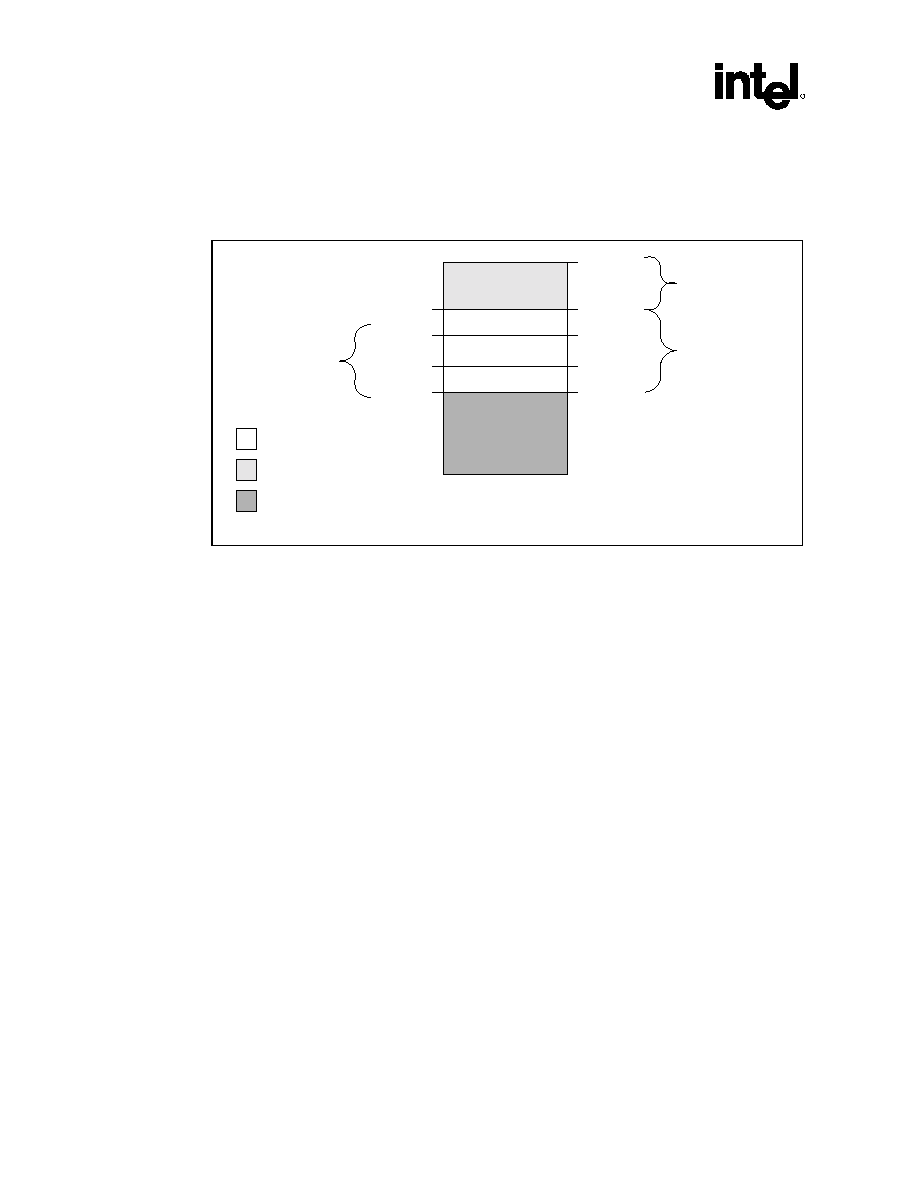
System Address Map
R
100
Intel
ģ
82845 MCH Datasheet
the same, since the PCI configuration portion of the BIOS software will program the TOM register
to the maximum value that is less than the amount of memory in the system and that allows enough
room for all populated PCI devices.
Figure 4. DOS Compatible Area Address Map
Monochrom e Display
Adapter Space
Upper, Lower,
Expansion Card BIOS
and Buffer Area
1 MB
sys_addr_map_2
640 KB
704 KB
736 KB
768 KB
0A0000h
0B0000h
0B8000h
0C0000h
Standard PCI/ISA
Video Mem ory
(SMM Mem ory)
Controlled by
PAM[6:0]
Controlled by
VGA Enable and
MDA Enable
= Optional AGP
= Optional System Mem ory
= System Mem ory
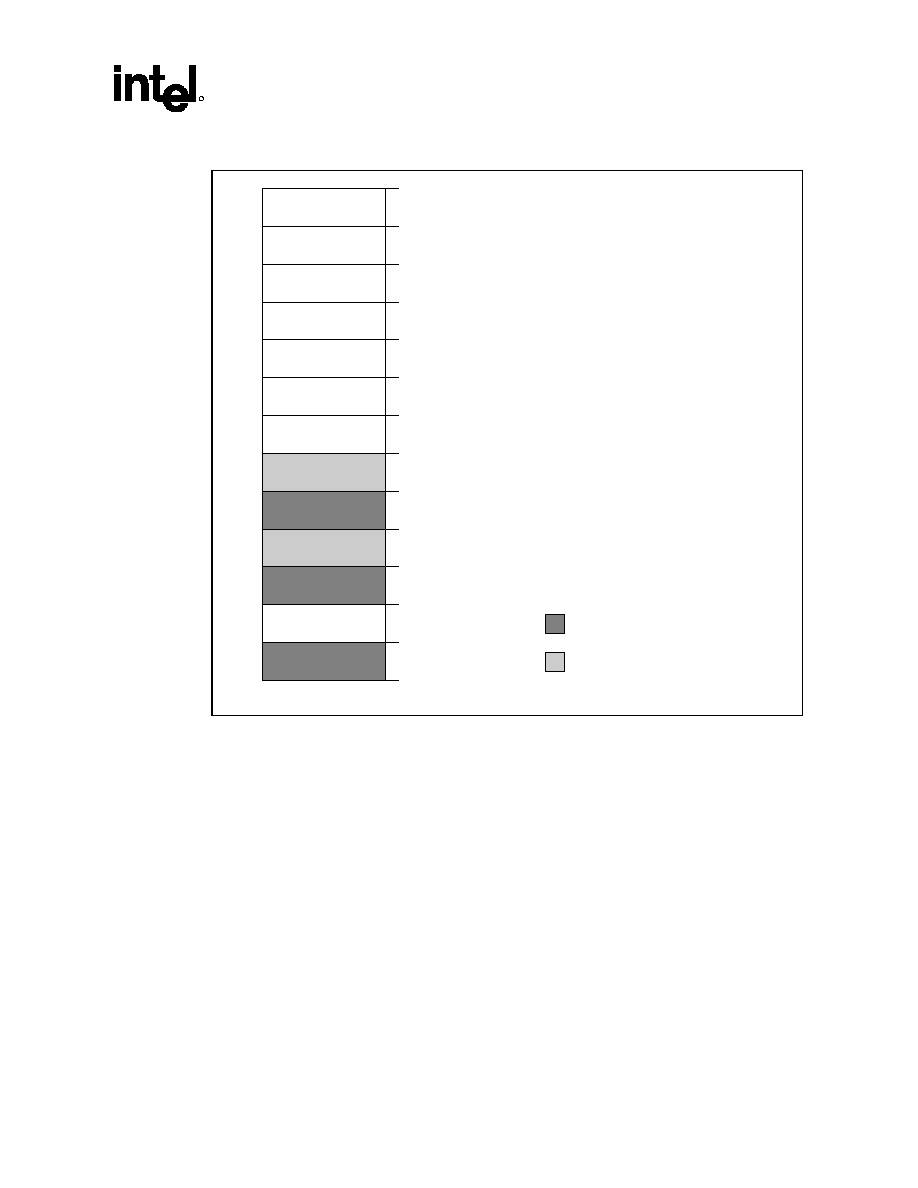
System Address Map
R
Intel
ģ
82845 MCH Datasheet 101
Figure 5. Extended Memory Range Address Map
= System Mem ory Region
= Optional System Mem ory Region
1_0000_0000 (4 GB)
FEF0_0000
FEE0_0000
FED0_0000
Top of Low Memory (TOM)
FEC0_0000
FEC8_0000
FF00_0000
100A_0000
100C_0000
00F0_0000 (15 MB)
0100_0000 (16 MB)
0010_0000 (1 MB)
TEM - TSEG
High BIOS, Optional
extended SMRAM
sys_addr_map_3
ISA Hole
Extended SMRAM
(translated to < 1 MB)
Extended SMRAM
Space
Local APIC Space
I/O APIC Space
I/O APIC Space
AGP/PCI
Hub Interface
(always)
Hub Interface
(always)

System Address Map
R
102
Intel
ģ
82845 MCH Datasheet
4.1.1
VGA and MDA Memory Space
Video cards use these legacy address ranges to map a frame buffer or a character-based video
buffer. The address ranges in this memory space are:
∑
VGAA
0_000A_0000 to 0_000A_FFFF
∑
MDA
0_000B_0000 to 0_000B_7FFF
∑
VGAB
0_000B_8000 to 0_000B_FFFF
By default, accesses to these ranges are forwarded to the hub interface. However, if the VGA_EN1
bit is set in the BCTRL1 configuration register, transactions within the VGA and MDA spaces are
sent to AGP. If the MCHCFG.MDAP configuration bit is set, accesses that fall within the MDA
range are sent to the hub interface independent of the setting of the VGA_EN1 bit.
If the MCHCFG.MDAP configuration bit is set, accesses in the MDA range are sent to the hub
interface, independent of the setting of the VGA_EN1 bit. Legacy support requires the ability to
have a second graphics controller (monochrome) in the system. In an 845E chipset system,
accesses in the standard VGA range are forwarded to AGP. Since the monochrome adapter may be
on the hub interface or (or ISA) bus, the MCH must decode cycles in the MDA range and forward
them to the hub interface. This capability is controlled by a configuration bit (MCHCFG.MDAP).
In addition to the memory range B0000h to B7FFFh, the MCH decodes I/O cycles at 3B4h, 3B5h,
3B8h, 3B9h, 3BAh, and 3BFh and forwards them to the hub interface.
An optimization allows the system to reclaim the memory displaced by these regions. If SMM
memory space is enabled by SMRAM.G_SMRARE and either the SMRAM.D_OPEN bit is set or
the system bus receives an SMM-encoded request for code (not data), then the transaction is
steered to system memory rather than the hub interface. Under these conditions, the VGA_EN1 bit
and the MDAP bit are ignored.

System Address Map
R
Intel
ģ
82845 MCH Datasheet 103
4.1.2
PAM Memory Spaces
The address ranges in this memory space are:
∑
PAMC0
0_000C_0000 to 0_000C_3FFF
∑
PAMC4
0_000C_4000 to 0_000C_7FFF
∑
PAMC8
0_000C_8000 to _000C_BFFF
∑
PAMCC
0_000C_C000 to 0_000C_FFFF
∑
PAMD0
0_000D_0000 to 0_000D_3FFF
∑
PAMD4
0_000D_4000 to 0_000D_7FFF
∑
PAMD8
0_000D_8000 to 0_000D_BFFF
∑
PAMDC
0_000D_C000 to 0_000D_FFFF
∑
PAME0
0_000E_0000 to 0_000E_3FFF
∑
PAME4
0_000E_4000 to 0_000E_7FFF
∑
PAME8
0_000E_8000 to 0_000E_BFFF
∑
PAMEC 0_000E_C000
to
0_000E_FFFF
∑
PAMF0
0_000F_0000 to 0_000F_FFFF
The 256-KB PAM region is divided into three parts:
∑
ISA expansion region; 128 KB area between 0_000C_0000h≠0_000D_FFFFh
∑
Extended BIOS region; 64 KB area between 0_000E_0000h≠0_000E_FFFFh
∑
System BIOS region; 64 KB area between 0_000F_0000h≠0_000F_FFFFh.
The ISA expansion region is divided into eight, 16-KB segments. Each segment can be assigned
one of four read/write states: read-only, write-only, read/write, or disabled. Typically, these blocks
are mapped through MCH and are subtractively decoded to ISA space.
The extended system BIOS region is divided into four, 16-KB segments. Each segment can be
assigned independent read and write attributes so it can be mapped either to main system memory
or to the hub interface. Typically, this area is used for RAM or ROM.
The system BIOS region is a single, 64-KB segment. This segment can be assigned read and write
attributes. It is by default (after reset) read/write disabled and cycles are forwarded to the hub
interface. By manipulating the read/write attributes, the MCH can "shadow" BIOS into system
memory.

System Address Map
R
104
Intel
ģ
82845 MCH Datasheet
4.1.3
ISA Hole Memory Space
BIOS software may optionally open a "window" between 15 MB and 16 MB (0_00F0_0000h to
0_00FF_FFFFh) that relays transactions to the hub interface instead of completing them with a
system memory access. This window is opened by programming the FDHC.HEN configuration
field.
4.1.4
TSEG SMM Memory Space
The TSEG SMM space (TOM ≠ TSEG to TOM) allows system management software to partition
a region of system memory just below the top of low memory (TOM) that is accessible only by
system management software. This region may be 128 KB, 256 KB, 512 KB, or 1 MB in size,
depending on the ESMRAMC.TSEG_SZ field. SMM memory is globally enabled by
SMRAM.G_SMRAME. Requests can access SMM system memory when either SMM space is
open (SMRAM.D_OPEN) or the MCH receives an SMM code request on its system bus. To
access the TSEG SMM space, TSEG must be enabled by ESMRAMC.T_EN. When all of these
conditions are met, then a system bus access to the TSEG space (between TOM≠TSEG and TOM)
is sent to system memory. If the high SMRAM is not enabled or if the TSEG is not enabled, then
all memory requests from all interfaces are forwarded to system memory. If the TSEG SMM space
is enabled, and an agent attempts a non-SMM access to TSEG space, then the transaction is
specially terminated.
Note: Hub interface and AGP originated accesses are not allowed to SMM space.
4.1.5
IOAPIC Memory Space
The IOAPIC space (0_FEC0_0000h to 0_FEC7_FFFFh) is used to communicate with IOAPIC
interrupt controllers that may be populated on the hub interface. Since it is difficult to relocate an
interrupt controller using plug-and-play software, fixed address decode regions have been
allocated for them. Processor accesses to the IOAPIC0 region are always sent to the hub interface.
4.1.6
System Bus Interrupt APIC Memory Space
The system bus interrupt space (0_FEE0_0000h to 0_FEEF_FFFFh) is the address used to deliver
interrupts to the system bus. Any device on AGP may issue a memory write to 0FEEx_xxxxh. The
MCH forwards this memory write, along with the data, to the system bus as an Interrupt Message
Transaction. The MCH terminates the system bus transaction by providing the response and
asserting TRDY#. This memory write cycle does not go to system memory.
4.1.7
High SMM Memory Space
The HIGHSMM space (0_FEDA_0000h to 0_FEDB_FFFFh) allows cacheable access to the
compatible SMM space by re-mapping valid SMM accesses between 0_FEDA_0000 and
0_FEDB_FFFF to accesses between 0_000A_0000 and 0_000B_FFFF. The accesses are
remapped when SMRAM space is enabled; an appropriate access is detected on the system bus,
and when ESMRAMC.H_SMRAME allows access to high SMRAM space. SMM memory

System Address Map
R
Intel
ģ
82845 MCH Datasheet 105
accesses from any hub interface or AGP are specially terminated: reads are provided with the
value from address 0 while writes are ignored entirely.
4.1.8
AGP Aperture Space (Device 0 BAR)
Processors and AGP devices communicate through a special buffer called the "graphics aperture"
(APBASE to APBASE + APSIZE). This aperture acts as a window into main system memory and
is defined by the APBASE and APSIZE configuration registers of the MCH. Note that the AGP
aperture must be above the top of memory and must not intersect with any other address space.
4.1.9
AGP Memory and Prefetchable Memory
Plug-and-play software configures the AGP memory window to provide enough memory space for
the devices behind this PCI-to-PCI bridge. Accesses whose addresses fall within this window are
decoded and forwarded to AGP for completion. The address ranges are:
∑
M1
MBASE1 to MLIMIT1
∑
PM1
PMBASE1 to PMLIMIT1
Note that these registers must be programmed with values that place the AGP memory space
window between the value in the TOM register and 4 GB. In addition, neither region should
overlap with any other fixed or relocatable area of memory.
4.1.10
Hub Interface Subtractive Decode
All accesses that fall between the value programmed into the TOM register and 4 GB
(i.e., TOM to 4 GB) are subtractively decoded and forwarded to the hub interface if they do not
decode to a space that corresponds to another device.
4.2
AGP Memory Address Ranges
The MCH can be programmed to direct memory accesses to the AGP bus interface when
addresses are within either of two ranges specified via registers in MCH device 1 configuration
space. The first range is controlled via the Memory Base Address (MBASE1) register and
Memory Limit Address (MLIMIT1) register. The second range is controlled via the Prefetchable
Memory Base Address (PMBASE1) register and Prefetchable Memory Limit Address
(PMLIMIT1) register
The MCH positively decodes memory accesses to AGP memory address space as defined by the
following equations:
∑
Memory_Base_Address
Address
Memory_Limit_Address
∑
Prefetchable_Memory_Base_Address
Address
Prefetchable_Memory_Limit_Address
The plug-and-play configuration software programs the effective size of the range and it depends
on the size of memory claimed by the AGP device.

System Address Map
R
106
Intel
ģ
82845 MCH Datasheet
Note: The MCH device 1 memory range registers described above are used to allocate memory address
space for any devices sitting on AGP bus that require such a window.
4.2.1
AGP DRAM Graphics Aperture
Memory-mapped, graphics data structures can reside in a Graphics Aperture to system memory.
This aperture is an address range defined by the APBASE and APSIZE registers of the MCH
device 0. The APBASE register follows the standard base address register template as defined by
the PCI Local Bus Specification, Revision 2.1. The size of the range claimed by the APBASE is
programmed via "back-end" register APSIZE (programmed by the chipset specific BIOS before
plug-and-play session is performed). APSIZE allows the BIOS software to pre-configure the
aperture size to be 4 MB, 8 MB, 16 MB, 32 MB, 64 MB, 128 MB or 256 MB. By programming
APSIZE to a specific size, the corresponding lower bits of APBASE are forced to 0 (behave as
hardwired). The default value of APSIZE forces an aperture size of 256 MB. The aperture address
range is naturally aligned.
Accesses within the aperture range are forwarded to the system memory subsystem. The MCH
translates the originally issued addresses via a translation table maintained in system memory. The
aperture range should be programmed as non-cacheable in the processor caches.
Note: Plug-and-play software configuration model does not allow overlap of different address ranges.
Therefore
the AGP Graphics Aperture and AGP memory address range are independent address
ranges that may abut, but cannot overlap one another.
4.3
System Management Mode (SMM) Memory Range
The MCH supports the use of system memory as System Management RAM (SMRAM) enabling
the use of System Management Mode. The MCH supports three SMRAM options: Compatible
SMRAM (C_SMRAM), High Segment (HSEG), and Top of Memory Segment (TSEG). System
Management RAM (SMRAM) space provides a memory area that is available for the SMI
handler's and code and data storage. This memory resource is normally hidden from the system
OS so that the processor has immediate access to this memory space upon entry to SMM. The
MCH provides three SMRAM options:
∑
Below 1- MB option that supports compatible SMI handlers.
∑
Above 1-MB option that allows new SMI handlers to execute with write-back cacheable
SMRAM.
∑
Optional larger write-back cacheable T_SEG area from 128 KB to 1 MB in size above 1 MB
that is reserved from the highest area in system memory. The above 1-MB solutions require
changes to compatible SMRAM handlers' code to properly execute above 1 MB.
Note: Masters from the hub interface and AGP are not allowed to access the SMM space.

System Address Map
R
Intel
ģ
82845 MCH Datasheet 107
4.3.1
SMM Space Definition
Its addressed SMM space and its DRAM SMM space define SMM space. The addressed SMM
space is defined as the range of bus addresses used by the processor to access SMM space. System
memory SMM space is defined as the range of physical system memory locations containing the
SMM code. SMM space can be accessed at one of three transaction address ranges: Compatible,
High, and TSEG. The Compatible and TSEG SMM space is not remapped and, therefore, the
addressed and DRAM SMM space is the same address range. Since the High SMM space is
remapped the addressed and system memory SMM space is a different address range. Note that the
High system memory space is the same as the Compatible Transaction Address space. Therefore,
the table below describes three unique address ranges:
∑
Compatible Transaction Address
∑
High Transaction Address
∑
TSEG Transaction Address
Table 11. SMM Space Address Ranges
SMM Space Enabled
Transaction Address Space
System Memory Space
Compatible
A0000h to BFFFFh
A0000h to BFFFFh
High
0FEDA0000h to 0FEDBFFFFh
A0000h to BFFFFh
TSEG
(TOM≠TSEG_SZ) to TOM
(TOM≠TSEG_SZ) to TOM
Note: High SMM: This is different than in some previous chipsets where the High segment was the
384-KB region from A0000h to FFFFFh.
Note: TSEG SMM: Note that this is different than in previous chipsets where the TSEG address space
was offset by 256 MB to allow for simpler decoding and the TSEG was remapped to just under the
TOM. In the MCH the 256 MB does not offset the TSEG region and it is not remapped.
4.3.2
SMM Space Restrictions
If any of the following conditions are violated, the results of SMM accesses are unpredictable and
may cause the system to hang:
∑
The Compatible SMM space must not be setup as cacheable.
∑
High or TSEG SMM transaction address space must not overlap address space assigned to
system memory, the AGP aperture range, or to any "PCI" devices (including hub interface and
AGP devices). This is a BIOS responsibility.
∑
Both D_OPEN and D_CLOSE must not be set to 1 at the same time.
∑
When TSEG SMM space is enabled, the TSEG space must not be reported to the OS as
available system memory. This is a BIOS responsibility.
∑
Any address translated through the AGP Aperture GTLB must not target system memory from
000A0000h to 000FFFFFh.

System Address Map
R
108
Intel
ģ
82845 MCH Datasheet
4.4
I/O Address Space
The MCH does not support the existence of any other I/O devices beside itself on the system bus.
The MCH generates either hub interface or AGP bus cycles for all processor I/O accesses. The
MCH contains two internal registers in the processor I/O space: Configuration Address
(CONF_ADDR) register and Configuration Data (CONF_DATA) register. These locations are
used to implement the PCI configuration space access mechanism and as described in Chapter 3.
The processor allows 64 KB+3 bytes to be addressed within the I/O space. The MCH propagates
the processor I/O address without any translation on to the destination bus and therefore provides
addressability for 64 KB+3 byte locations. Note that the upper 3 locations can be accessed only
during I/O address wrap-around when signal A16# address signal is asserted. A16# is asserted on
the system bus whenever an I/O access is made to 4 bytes from address 0FFFDh, 0FFFEh, or
0FFFFh. A16# is also asserted when an I/O access is made to 2 bytes from address 0FFFFh.
The I/O accesses (other than ones used for configuration space access) are forwarded normally to
the hub interface unless they fall within the AGP I/O address range as defined by the mechanisms
explained below. The MCH does not post I/O write cycles to IDE.
The MCH never responds to I/O or configuration cycles initiated on AGP or the hub interface.
Hub interface transactions requiring completion are terminated with "master abort" completion
packets on the hub interface. Hub interface write transactions not requiring completion are
dropped. AGP/PCI I/O reads are never acknowledged by the MCH.
4.5
MCH Decode Rules and Cross-Bridge Address
Mapping
The address map described above applies globally to accesses arriving on any of the three
interfaces (i.e., processor system bus, hub interface, or AGP).
4.5.1
Hub Interface Decode Rules
The MCH accepts accesses from the hub interface with the following address ranges:
∑
All memory read and write accesses to main DRAM (except SMM space).
∑
All memory write accesses from the hub interface to AGP memory range defined by
MBASE1, MLIMIT1, PMBASE1, and PMLIMIT1.
∑
All memory read/write accesses to the Graphics Aperture defined by APBASE and APSIZE.
∑
Memory writes to VGA range on AGP if enabled.
All memory reads from the hub interface that target >4-GB memory range are terminated with a
master abort completion, and all memory writes (>4 GB) from the hub interface are ignored.

System Address Map
R
Intel
ģ
82845 MCH Datasheet 109
4.5.2
AGP Interface Decode Rules
Cycles Initiated Using AGP FRAME# Protocol
The MCH does not support any AGP FRAME# access targeting the hub interface. The MCH
claims AGP-initiated memory read and write transactions decoded to the system memory range or
the Graphics Aperture range. All other memory read and write requests will be master-aborted by
the AGP initiator as a consequence of MCH not responding to a transaction.
Under certain conditions, the MCH restricts access to the DOS Compatibility ranges governed by
the PAM registers by distinguishing access type and destination bus. The MCH does NOT accept
AGP FRAME# write transactions to the compatibility ranges if the PAM designates system
memory as writeable. If accesses to a range are not write-enabled by the PAM, the MCH does not
respond and the cycle results in a master-abort. The MCH accepts AGP FRAME# read
transactions to the compatibility ranges if the PAM designates system memory as readable. If
accesses to a range are not read-enabled by the PAM, the MCH does not respond and the cycle
results in a master-abort.
If agent on AGP issues an I/O, PCI Configuration or PCI Special Cycle transaction, the MCH does
not respond and cycle results in a master-abort.
Cycles Initiated Using AGP PIPE# or SB Protocol
All cycles must reference system memory; that is, system memory address range (including PAM)
or Graphics Aperture range (also physically mapped within system memory but using different
address range). AGP accesses to SMM space are not allowed. AGP-initiated cycles that target
system memory are not snooped on the host bus, even if they fall outside of the AGP aperture
range.
If a cycle is outside of the system memory range, then it terminates as follows:
∑
Reads remap to memory address 0h, return data from address 0h, and set the IAAF error bit in
ERRSTS register in device 0
∑
Writes are terminated internally without affecting any chip signals or system memory
AGP Accesses to MCH that Cross Device Boundaries
For AGP FRAME# accesses, when an AGP master gets disconnected, it resumes at the new
address which allows the cycle to be routed to or claimed by the new target. Therefore, the target
on potential device boundaries should disconnect accesses. The MCH disconnects AGP FRAME#
transactions on 4-KB boundaries.
AGP PIPE# and SBA accesses are limited to 256 bytes and must hit system memory. Read
accesses crossing a device boundary will return invalid data when the access crosses out of system
memory. Write accesses crossing out of system memory will be discarded. The IAAF Error bit will
be set.

System Address Map
R
110
Intel
ģ
82845 MCH Datasheet
This page is intentionally left blank.

Functional Description
R
Intel
ģ
82845 MCH Datasheet 111
5 Functional
Description
This chapter describes the system bus that connects the MCH to the processor, the system memory
interface, the AGP interface, the MCH power and thermal management, the MCH clocking, and
the MCH system reset and power sequencing.
5.1 System
Bus
The MCH supports the Pentium 4 processor subset of the Enhanced Mode Scaleable Bus. Source
synchronous transfers are used for the address and data signals. The address signals are double
pumped and a new address can be generated every other bus clock. At 100-MHz bus frequency,
the address signals run at 200 MT/s for a maximum address queue rate of 50-M addresses/sec. The
data is quad pumped and an entire 64-byte cache line can be transferred in two bus clocks. At
100/133-MHz bus frequency, the data signals run at 400/533 MT/s for a maximum bandwidth of
3.2/4.2 GB/s. The MCH supports a 12-deep IOQ.
The MCH supports two outstanding deferred transactions on the system bus. The two transactions
must target different I/O interfaces as only one deferred transaction can be outstanding to any
single I/O interface at a time.
5.1.1
Dynamic Bus Inversion
The MCH supports Dynamic Bus Inversion (DBI) when driving and receiving data from the
system bus. DBI limits the number of data signals that are driven to a low voltage on each quad
pumped data phase. This decreases the power consumption of the MCH. DBI[3:0]# indicates if the
corresponding 16 bits of data are inverted on the bus for each quad pumped data phase:
DBI[3:0]# Data
Bits
DBI0# HD[15:0]#
DBI1# HD[31:16]#
DBI2# HD[47:32]#
DBI3# HD[63:48]#
When the processor or the MCH drives data, each 16-bit segment is analyzed. If more than 8 of
the 16 signals would normally be driven low on the bus, the corresponding DBI# signal will be
asserted and the data will be inverted prior to being driven on the bus. When the processor or the
MCH receives data, it monitors DBI[3:0]# to determine if the corresponding data segment should
be inverted.

Functional Description
R
112
Intel
ģ
82845 MCH Datasheet
5.1.2
System Bus Interrupt Delivery
The Pentium 4 processor supports the system bus interrupt delivery; the APIC serial bus interrupt
delivery mechanism is not supported. Interrupt-related messages are encoded on the system bus as
"Interrupt Message Transactions". In an 845E chipset platform, system bus interrupts can originate
from the processor on the system bus, or from a downstream device on the hub interface or AGP.
In the later case the MCH drives the "Interrupt Message Transaction" onto the system bus.
In an 845E chipset platform, the ICH4 contains IOxAPICs, and its interrupts are generated as
upstream hub interface memory writes. Furthermore, PCI 2.2 defines MSIs (Message Signaled
Interrupts) that are also in the form of memory writes. A PCI 2.2 device can generate an interrupt
as an MSI cycle on it's PCI bus, instead of asserting a hardware signal to the IOxAPIC. The MSI
can be directed to the IOxAPIC, which in turn generates an interrupt as an upstream hub interface
memory write. Alternatively, the MSI can be directed directly to the system bus. The target of a
MSI is dependent on the address of the interrupt memory write. The MCH forwards inbound hub
interface and AGP (PCI semantic only) memory writes to address 0FEEx_xxxxh, to the system bus
as "Interrupt Message Transactions".
5.1.3
Upstream Interrupt Messages
The MCH accepts message-based interrupts from AGP (PCI semantics only) or its hub interface
and forwards them to the system bus as Interrupt Message Transactions. The interrupt messages
presented to the MCH are in the form of memory writes to address 0FEEx_xxxxh. At the hub
interface or AGP interface, the memory write interrupt message is treated like any other memory
write; it is either posted to the inbound data buffer (if space is available) or retried (if data buffer
space is not immediately available). Once posted, the memory write from AGP or the hub interface
to address 0FEEx_xxxxh is decoded as a cycle that needs to be propagated by the MCH to the
system bus as an Interrupt Message Transaction.

Functional Description
R
Intel
ģ
82845 MCH Datasheet 113
5.2
System Memory Interface
The 845E chipset can be configured to support DDR200/266 memory.
5.2.1
Double Data Rate (DDR) SDRAM Interface Overview
The MCH integrates a system memory SDRAM controller with a 64-bit wide interface and twelve
system memory clock signals.
The MCH includes support for:
∑
Up to 2 GB of 200/266 MHz DDR SDRAM
∑
DDR200/266 unbuffered 184 pin DDR SDRAM DIMMs
∑
Maximum of two DIMMs, single-sided and/or double-sided
∑
Configurable optional ECC
The two bank-select lines SBS[1:0] and the thirteen address lines (SMA[12:0]) allow the MCH to
support 64-bit wide DIMMs using 64-Mb, 128-Mb, 256-Mb, and 512-Mb SDRAM technologies.
While address lines SMA[9:0] determine the starting address for a burst, burst lengths are fixed at
four. Four chip selects SCS# lines allow a maximum of two rows with single-sided SDRAM
DIMMs and four rows with double-sided SDRAM DIMMs.
The MCH's system memory controller targets CAS latencies of 2 and 2.5 clocks for SDRAM. The
MCH provides refresh functionality with a programmable rate (normal SDRAM rate is
1 refresh/15.6 Ķs).
5.2.2
Memory Organization and Configuration
In the following discussion the term row refers to a set of memory devices that are simultaneously
selected by a SCS# signal. The MCH supports a maximum of four rows of memory. For the
purposes of this discussion, a "side" of a DIMM is equivalent to a "row" of SDRAM devices.
Table 12. Supported DIMM Configurations
Density
64 Mbit
128 Mbit
256 Mbit
512 Mbit
Device
Width
X8 X16 X8 X16 X8 X16 X8 X16
Single \
Double
SS/DS SS/DS SS/DS SS/DS SS/DS SS/DS SS/DS SS/DS
184 pin
DDR
DIMMs
64 MB /
128 MB
32 MB /
NA
128 MB /
256 MB
64 MB /
NA
256 MB /
512 MB
128 MB /
NA
512 MB /
1024 MB
256 MB /
NA
NOTE: Double-sided X16 DDR SDRAM devices are not supported.

Functional Description
R
114
Intel
ģ
82845 MCH Datasheet
5.2.2.1
Configuration Mechanism for DIMMs
Detection of the type of SDRAM installed on the DIMM is supported via a Serial Presence Detect
mechanism as defined in the JEDEC 184-Pin Unbuffered DDR-DIMM Specification. This uses
the SCL, SDA and SA[2:0] pins on the DIMMs to detect the type and size of the installed DIMMs.
No special programmable modes
are provided on the MCH for detecting the size and type of
memory installed. Type and size detection must be done via the serial presence detection pins.
Memory Detection and Initialization
Before any cycles to the memory interface can be supported, the MCH SDRAM registers must be
initialized. The MCH must be configured for operation with the installed memory types. Detection
of memory type and size is accomplished via the System Management Bus (SMBus) interface on
the ICH4. This two-wire bus is used to extract the SDRAM type and size information from the
Serial Presence Detect port on the SDRAM DIMMs. SDRAM DIMMs contain a 5-pin Serial
Presence Detect interface, including SCL (serial clock), SDA (serial data), and SA[2:0]. Devices
on the SMBus bus have a seven-bit address. For the SDRAM DIMMs, the upper four bits are
fixed at 1010. The lower three bits are strapped on the SA[2:0] pins. SCL and SDA are connected
directly to the system management bus on the ICH4. Thus, data is read from the Serial Presence
Detect port on the DIMMs via a series of I/O cycles to the ICH4. BIOS needs to determine the
size and type of memory used for each of the rows of memory to properly configure the MCH
memory interface.
SMBus Configuration and Access of the Serial Presence Detect Ports
For more details on SMBus Configuration and Serial Present Detect Ports, see the Intel
ģ
82801DB
I/O Controller Hub 4 (ICH4) Datasheet.
Memory Register Programming
This section provides an overview of how the required information for programming the SDRAM
registers is obtained from the Serial Presence Detect ports on the DIMMs. The Serial Presence
Detect ports are used to determine refresh rate, MA and MD buffer strength, row type (on a row by
row basis), SDRAM Timings, row sizes, and row page sizes. Table 13 lists a subset of the data
available through the on-board Serial Presence Detect ROM on each DIMM.
Table 13. Data Bytes on DIMM Used for Programming DRAM Registers
Byte Function
2
Memory type (SDR SDRAM or DDR SDRAM)
3
Number of row addresses, not counting bank addresses
4
Number of column addresses
5
Number of banks of SDRAM (single- or double-sided DIMM)
11
ECC, no ECC
12 Refresh
rate
17
Number banks on each device
Table 13 is only a subset of the defined SPD bytes on the DIMMs. These bytes collectively
provide enough data for programming the MCH SDRAM registers.

Functional Description
R
Intel
ģ
82845 MCH Datasheet 115
5.2.3
Memory Address Translation and Decoding
The 845E MCH contains address decoders that translate the address received on the system bus or
the hub interface. Decoding and translation of these addresses vary with the four SDRAM types.
Also, the number of pages, page sizes, and densities supported vary with the type. In general, the
MCH supports 64-Mb, 128-Mb, 256-Mb, and 512-Mb SDRAM devices. The multiplexed
row/column address
to
the SDRAM memory array is provided by the SBS[1:0] and SMA[12:0]
signals. These addresses are derived from the system address bus as defined by Table 14 for
SDRAM devices.
Table 14. Address Translation and Decoding
Tech Configuration Row
size
Page size
Row / Column
/ Bank
Addr BA1 BA0 A12 A11 A10 A9 A8 A7 A6 A5 A4 A3 A2 A1 A0
64Mb
1Meg x 16 x 4bks
32 MB
12x8x2
Row
24
11 12 24 13 14 15 16 23 22 21 20 19 18 17
2
KB
Col
AP 10 9 8 7 6 5 4 3
64Mb
2Meg x 8 x 4bks
64 MB
12x9x2
Row
25
13 12 24 25 14 15 16 23 22 21 20 19 18 17
4
KB
Col
AP 11
10 9 8 7 6 5 4 3
128Mb 2Meg x 16 x 4bks
64 MB
12x9x2
Row
25
13 12 24 25 14 15 16 23 22 21 20 19 18 17
4
KB
Col
AP 11
10 9 8 7 6 5 4 3
128Mb 4Meg x 8 x 4bks
128 MB
12x10x2 Row
26
14 13 26 25 24 15 16 23 22 21 20 19 18 17
8
KB
Col
AP
12
11
10 9 8 7 6 5 4 3
256Mb 4Meg x 16 x 4bks
128 MB
13x9x2
Row
26
13 12 26 24 25 14 15 16 23 22 21 20 19 18 17
4
KB
Col
AP 11
10 9 8 7 6 5 4 3
256Mb 8Meg x 8 x 4bks
256 MB
13x10x2 Row
27
14 13 27 26 25 24 15 16 23 22 21 20 19 18 17
8
KB
Col
AP
12
11
10 9 8 7 6 5 4 3
512Mb 8Meg x 16 x 4bks
256 MB
13x10x2 Row
27
14 13 27 26 25 24 15 16 23 22 21 20 19 18 17
8
KB
Col
AP
12
11
10 9 8 7 6 5 4 3
512Mb 16Meg x 8 x 4bks
512 MB
13x11x2 Row
28
14 15 27 26 25 24 28 16 23 22 21 20 19 18 17
16
KB
Col
13 AP
12
11
10 9 8 7 6 5 4 3

Functional Description
R
116
Intel
ģ
82845 MCH Datasheet
5.2.4
DRAM Performance Description
The overall memory performance is controlled by the DRAM Timing (DRT) Register, pipelining
depth used in the MCH, memory speed grade, and the type of SDRAM used in the system. In
addition, the exact performance in a system is also dependent on the total memory supported,
external buffering, and memory array layout. The most important contribution to overall
performance by the system memory controller is to minimize the latency required to initiate and
complete requests to memory and to support the highest possible bandwidth (full streaming, quick
turn-arounds). One measure of performance is the total flight time to complete a cache line
request. A complete discussion of performance involves the entire chipset, not just the system
memory controller.
5.2.4.1
Data Integrity (ECC)
The MCH supports single-bit Error Correcting Code (or Error Checking and Correcting) and
multiple-bit EC (Error Checking) on the system memory interface. The MCH generates an 8-bit
code word for each 64-bit QWord of memory. The MCH performs two QWord writes at a time;
thus, two 8-bit codes are sent with each write. Since the code word covers a full QWord, writes of
less than a QWord require a read-merge-write operation. Consider a DWord write to memory. In
this case, when in ECC mode, the MCH reads the QWord where the addressed DWord will be
written, merges in the new DWord, generates a code covering the new QWord, and, finally, writes
the entire QWord and code back to memory. Any correctable (single-bit) errors detected during
the initial QWord read are corrected before merging the new DWord.
The MCH also supports EC (Error Checking) data integrity mode. In this mode, the MCH
generates and stores a code for each QWord of memory. It then checks the code for reads from
memory but does not correct any errors that are found. Thus, the read performance hit associated
with ECC is not incurred.
5.3
AGP Interface Overview
The MCH supports 1.5 V AGP 1x/2x/4x devices. The AGP signal buffers are 1.5 V drive/receive
(buffers are not 3.3 V tolerant). The MCH supports 2X/4X source synchronous clocking transfers
for read and write data, and sideband addressing. The MCH also support 2X and 4X clocking for
Fast Writes initiated from the MCH (on behalf of the processor).
AGP PIPE# or SBA[7:0] transactions to system memory do not get snooped and are, therefore, not
coherent with the processor caches. AGP FRAME# transactions to system memory are snooped.
AGP PIPE# and SBA[7:0] accesses to and from the hub interface are not supported. AGP
FRAME# access from an AGP master to the hub interface are also not supported. Only the AGP
FRAME memory writes from the hub interface are supported.
5.3.1
AGP Target Operations
As an initiator, the MCH does not initiate cycles using AGP enhanced protocols. The MCH
supports AGP cycles targeting the interface to system memory only. The MCH supports
interleaved AGP PIPE# and AGP FRAME#, or AGP SBA[7:0] and AGP FRAME# transactions.

Functional Description
R
Intel
ģ
82845 MCH Datasheet 117
Table 15. AGP Commands Supported by the MCH When Acting As an AGP Target
MCH Host Bridge
AGP
Command
C/BE[3:0]#
Encoding
Cycle Destination
Response as PCIx Target
Read
0000
System memory
Low-priority read
0000
Hub interface
Complete with random data
Hi-Priority Read
0001
System memory
High-priority read
0000
The Hub interface
Complete with random data
Reserved 0010
N/A
No
response
Reserved 0011
N/A
No
response
Write
0100
System memory
Low-priority write
0100
Hub interface
Cycle goes to DRAM with byte
enables inactive
Hi-Priority Write
0101
System memory
High-priority write
0101
Hub interface
Cycle goes to DRAM with byte
enables inactive; does not go to
the hub interface
Reserved 0110
N/A
No
response
Reserved 0111
N/A
No
response
Long Read
1000
System memory
Low-priority read
Hub interface
Complete locally with random data;
does not go to the hub interface
Hi-Priority Long
Read
1001 System
memory
High-priority
read
Hub interface
Complete with random data
Flush
1010
MCH
Complete with QW of random data
Reserved 1011
N/A
No
response
Fence
1100
MCH
No response; Flag inserted in
MCH request queue
Reserved 1101
N/A
No
response
Reserved 1110
N/A
No
response
Reserved 1111
N/A
No
response
NOTES:
1. N/A refers to a function that is not applicable
As a target of an AGP cycle, the MCH supports all the transactions targeting system memory
(summarized in Table 15). The MCH supports both normal and high-priority read and write
requests. The MCH does not support AGP cycles to the hub interface. PIPE# and SBA cycles do
not require coherency management and all AGP initiator accesses to system memory, using AGP
PIPE# or SBA protocol, are treated as non-snoopable cycles. These accesses are directed to the
AGP aperture in system memory that is programmed as either uncacheable (UC) memory or write
combining (WC) in the processor's MTRRs.

Functional Description
R
118
Intel
ģ
82845 MCH Datasheet
5.3.2
AGP Transaction Ordering
The MCH observes transaction ordering rules as defined by the AGP Interface Specification,
Revision 2.0.
5.3.3
AGP Signal Levels
The 4x data transfers use 1.5 V signaling levels as described by the AGP Interface Specification,
Revision 2.0. The MCH supports 1X/2X data transfers using 1.5 V signaling levels.
5.3.4
4X AGP Protocol
In addition to the 1X and 2X AGP protocol, the MCH supports 4X AGP read and write data
transfers and 4X sideband address generation. The 4X operation is compliant with the AGP
Interface Specification, Revision 2.0.
The MCH indicates that it supports 4X data transfers via bit 2 of the AGPSTAT.RATE field.
When bit 2 of the AGPCMD.DRATE field is set to 1 during system initialization, the MCH
performs AGP read/write data transactions using 4X protocol. This bit is not dynamic. Once this
bit is set during initialization, the data transfer rate must not be changed.
The 4X data rate transfer provides 1.06 GB/s transfer rates. The control signal protocol for the 4X
data transfer protocol is identical to 1X/2X protocol. In 4X mode 16 bytes of data are transferred
on every 66 MHz clock edge. The minimum throttleable block size remains four, 66-MHz clocks
(64 bytes of data are transferred per block). Three additional signal pins are required to implement
the 4X data transfer protocol. These signal pins are complimentary data transfer strobes for the AD
bus (2) and the SBA bus (1).
5.3.5 Fast
Writes
The MCH supports 2X and 4X Fast Writes from the MCH to the graphics controller on AGP. Fast
Write operation is compliant with Fast Writes as currently described in the AGP Interface
Specification, Revision 2.0. To use the Fast Write protocol, both AGPCTRL.FWCE and
AGPCMD.FWPE must be set to 1.
AGPCTRL.FWCE is set to 0 by default. When this bit is set to 1, the MCH indicates that it
supports Fast Writes through AGPSTAT.FW. When both AGPCMD.FWEN and
AGPCTRL.FWCE are set to 1, the MCH uses Fast Write protocol to transfer memory write data to
the AGP master.
Memory writes originating from the processor or from the hub interface use the Fast Write
protocol when it is both capability enabled and enabled. The data rate used to perform the Fast
Writes is dependent on the bits set in the AGPCMD.DRATE field (bits [2:0]).
If bit 2 of the AGPCMD.DRATE field is 1, the data transfers occur using 4X strobing.
If bit 1 of AGPCMD.DRATE field is 1, the data transfers occur using 2X strobing.
If bit 0 of AGPCMD.DRATE field is 1, Fast Writes are disabled and data transfers occur using
standard PCI protocol. Note that only one of the three DRATE bits can be set by initialization
software (Table 16).
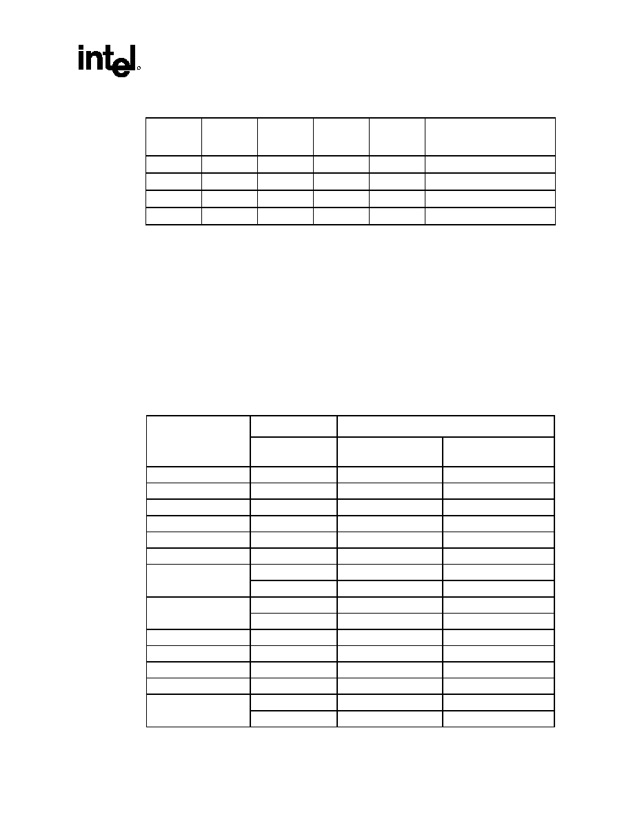
Functional Description
R
Intel
ģ
82845 MCH Datasheet 119
Table 16. Data Rate Control Bits
AGPCNTL
.FWCE
AGPCMD.
FWPE
AGPCMD.
DRATE
[bit 2]
AGPCMD.
DRATE
[bit 1]
AGPCMD.
DRATE
[bit 0]
MCH =>AGP Master Write
Protocol
0 0 X X X
1x
1 1 0 0 1
1x
1 1 0 1 0
2x
strobing
1 1 1 0 0
4x
strobing
5.3.6
AGP FRAME# Transactions on AGP
The MCH accepts and generates AGP FRAME# transactions on the AGP bus. The MCH
guarantees that AGP FRAME# accesses to system memory are kept coherent with the processor
caches by generating snoops to the host bus. LOCK#, SERR#, and PERR# signals are not
supported.
MCH Initiator and Target Operations
Table 17 summarizes MCH target operation for AGP FRAME# initiators. The cycles can be either
destined to system memory or the hub interface.
Table 17. PCI Commands Supported by the MCH When Acting As a FRAME# Target
C/BE[3:0]# Intel
ģ
82845 MCH
PCI Command
Encoding
Cycle Destination
Response As a FRAME#
Target
Interrupt Acknowledge
0000
N/A
No response
Special cycle
0001
N/A
No response
I/O Read
0010
N/A
No response
I/O Write
0011
N/A
No response
Reserved 0100
N/A
No
response
Reserved 0101
N/A
No
response
Memory Read
0110
System memory
Read
0110
Hub
interface
No
response
Memory Write
0111
System memory
Posts data
0111
Hub interface
No response
Reserved 1000
N/A
No
response
Reserved 1001
N/A
No
response
Configuration Read
1010
N/A
No response
Configuration Write
1011
N/A
No response
Memory Read Multiple
1100
System memory
Read
1100
Hub interface
No response

Functional Description
R
120
Intel
ģ
82845 MCH Datasheet
C/BE[3:0]# Intel
ģ
82845 MCH
PCI Command
Encoding
Cycle Destination
Response As a FRAME#
Target
Dual Address Cycle
1101
N/A
No response
Memory Read Line
1110
System Memory
Read
1110
Hub interface
No response
Memory Write and
Invalidate
1111
System memory
Posts data
1111
Hub
interface
Posts
Data
NOTES:
1. N/A refers to a function that is not applicable
As a target of an AGP FRAME# cycle, the MCH only supports the following transactions:
∑
Memory Read, Memory Read Line, and Memory Read Multiple. These commands are
supported identically by the MCH. The MCH does not support reads of the hub interface bus
from AGP.
∑
Memory Write and Memory Write and Invalidate. These commands are aliased and processed
identically.
∑
Other Commands. Other commands (e.g., I/O R/W and Configuration R/W) are not supported
by the MCH as a target and result in master abort.
∑
Exclusive Access. The MCH does not support PCI locked cycles as a target.
∑
Fast Back-to-Back Transactions. The MCH, as a target, supports fast back-to-back cycles
from an AGP FRAME# initiator.
As an initiator of AGP FRAME# cycle, the MCH only supports the following transactions:
∑
Memory Read and Memory Read Line. MCH supports reads from host to AGP. MCH does
not support reads from the hub interface to AGP.
∑
Memory Read Multiple. This command is not supported by the MCH as an AGP FRAME#
initiator.
∑
Memory Write. The MCH initiates AGP FRAME# cycles on behalf of the host or the hub
interface. As an initiator, the MCH does not issue Memory Write and Invalidate cycles. The
MCH does not support write merging or write collapsing. The MCH allows non-snoopable
write transactions from the hub interface to the AGP bus.
∑
I/O Read and Write. I/O read and write cycles from the host are sent to the AGP bus. The I/O
base and limit address range for the AGP bus are programmed in the configuration registers.
All other accesses that do not correspond to this programmed address range are forwarded to
the hub interface.
∑
Exclusive Access. The MCH does not issue a locked cycle on the AGP bus on behalf of either
the host or the hub interface. The hub interface and host locked transactions to AGP are
initiated as unlocked transactions by the MCH on the AGP bus.
∑
Configuration Read and Write. Host configuration cycles to AGP are forwarded as Type 1
configuration cycles.
∑
Fast Back-to-Back Transactions. The MCH, as an initiator, does not perform fast back-to-
back cycles.

Functional Description
R
Intel
ģ
82845 MCH Datasheet 121
MCH Retry/Disconnect Conditions
The MCH generates retry/disconnect according to the AGP Interface Specification, Revision 2.0
rules when being accessed as a target from the AGP FRAME# device.
Delayed Transaction
When an AGP FRAME#-to-system memory read cycle is retried by the MCH, it is processed
internally as a delayed transaction. The MCH supports the delayed transaction mechanism on the
AGP target interface for the transactions issued using AGP FRAME# protocol. This mechanism is
compatible with the PCI Local Bus Specification, Revision 2.1. The process of latching all
information required to complete the transaction, terminating with Retry, and completing the
request without holding the master in wait-states is called a delayed transaction.
The MCH latches the address and command when establishing a delayed transaction. The MCH
generates a delayed transaction on the AGP only for AGP FRAME# to system memory read
accesses. The MCH does not allow more than one delayed transaction access from AGP at any
time.
5.4
Power and Thermal Management
An 845E chipset platform is compliant with the following specifications:
∑
APM, Revision 1.2
∑
ACPI, Revision 1.0b
∑
PCI Power Management, Revision 1.0
∑
PC '99, Revision 1.0
∑
PC '99A
∑
PC '01, Revision 1.0
5.4.1
Processor Power State Control
∑
C0 (Full On): This is the only state that runs software. All clocks are running, STPCLK# is
deasserted, and the processor core is active. The processor can service snoops and maintain
cache coherency in this state.
∑
Stop-Grant State: This function can be enabled or disabled via a configuration bit. When
this function is enabled, STPCLK# is asserted to place the processor into the C2 state with a
programmable duty cycle. This is an ACPI defined function but BIOS or APM (via BIOS) can
use this facility.

Functional Description
R
122
Intel
ģ
82845 MCH Datasheet
5.4.2
Sleep State Control
∑
S0 (Awake): In this state all power planes are active. All of the ACPI software "C" states are
embedded in this state.
∑
S1: The recommended implementation of S1 state is the same as C2 state (Stop Grant), which
is entered by the assertion of the STPCLK# signal from the ICH4 to the processor. A further
power saving can be achieved by asserting processor SLP# from the ICH4. This puts the
processor into Sleep State.
∑
S2: ACPI S2 state is not supported in the 845E chipset desktop platform.
∑
S3 (Suspend To RAM (STR)): The next level of power reduction occurs when the clock
synthesizers and main power planes (ICH4, MCH, and the processor) are shut down but the
system memory plane and the ICH4 resume well remain active. This is the Suspend-to-RAM
(STR) state. All clocks from synthesizers are shut down during the S3 state.
∑
S4 and S5 (Suspend To Disk (STD), Soft Off): The next level of power reduction occurs
when the memory power and MCH are shut down in addition to the clock synthesizers, ICH4,
and the processor power planes. The ICH4 resume well is still powered.
∑
G3 (Mechanical Off): In this state only the RTC well is powered. The system can only
reactivate when the power switch is returned to the "On" position.
5.5 MCH
Clocking
The 845E chipset is supported by the CK_408 compliant clock synthesizer. For details on
clocking, refer to the Intel
ģ
Pentium 4 Processor in a 478-Pin Package and Intel
ģ
845E Chipset
Platform For DDR Design Guide.
5.6
MCH System Reset and Power Sequencing
For details on MCH system reset and power sequencing, refer to the Intel
ģ
Pentium 4 Processor in
a 478-Pin Package and Intel
ģ
845E Chipset Platform For DDR Design Guide.

Electrical Characteristics
R
Intel
ģ
82845 MCH Datasheet 123
6 Electrical
Characteristics
This chapter contains the absolute maximum operating ratings, power characteristics, and DC
characteristics for the 82845 MCH.
6.1
Absolute Maximum Ratings
Table 18 lists the MCH's maximum environmental stress ratings. Functional operation at the
absolute maximum and minimum is neither implied nor guaranteed. Functional operating
parameters are listed in the DC tables.
Warning: Stressing the device beyond the "Absolute Maximum Ratings" may cause permanent damage.
These are stress ratings only. Operating beyond the "operating conditions" is not recommended
and extended exposure beyond "operating conditions" may affect reliability.
Table 18. Absolute Maximum Ratings
Symbol Parameter Min
Max
Unit
Notes
Tstorage Storage
Temperature
-55
150
į
C
VCC1_5
1.5 V Supply Voltage with respect to VSS
-0.72
2.3
V
VCC1_8
1.8 V Supply Voltage with respect to VSS
-0.88
2.69
V
VCCSM
2.5 V DDR Supply Voltage with respect to
VSS
-3.60 6.3 V
VTT
AGTL+ buffer DC input voltage with respect
to VSS
-0.55 2.3 V
V
IL,
V
IH
(DDR)
Voltage on 2.5 V DDR tolerant input pins with
respect to VSS
-3.60 6.30

Electrical Characteristics
R
124
Intel
ģ
82845 MCH Datasheet
6.2 Power
Characteristics
Table 19. Power Characteristics
Symbol Parameter Min
Type
Max
Unit
Notes
I
VTT
Intel
ģ
845E Chipset MCH VTT Supply
Current
2.4
A
I
VCC1_5_CORE
1.5 V Core Supply Current
1.9
A
1
I
VCC1_5_AGP
1.5 V AGP Supply Current
0.37
A
1
I
VCC1_8
1.8 V Hub Interface Supply Current
0.20
A
HVREF, AGPREF, HI_REF Supply
Currents
10
mA
I
VCCSM
DDR System Memory Interface
(2.5 V) Supply Current
1.9
A
I
SUS_VCCSM
DDR System Memory Interface
(2.5 V) Standby Supply Current
25
mA
I
SDREF
DDR System Memory Interface
Reference Voltage (1.25 V) Supply
Current
10
mA
I
SUS_SDREF
DDR System Memory Interface
Reference Voltage (1.25 V) Standby
Supply Current
1
mA
I
TTRC
DDR System Memory Interface
Resister Compensation Voltage
(1.25 V) Supply Current
40
mA
I
SUS_TTRC
DDR System Memory Interface
Resister Compensation Voltage
(1.25 V) Standby Supply Current
0
mA
NOTES:
1. These current levels can happen simultaneously, and can be summed into one supply.
6.3 Signal
Groups
The signal description includes the type of buffer used for the particular signal:
AGTL+
Open Drain AGTL+ interface signal. Refer to the AGTL+ I/O Specification for
complete details. The MCH integrates most AGTL+ termination resistors.
AGP
AGP interface signals. These signals are compatible with AGP 2.0 1.5 V
Signaling Environment DC and AC Specifications. The buffers are not 3.3 V
tolerant.
HI CMOS
Hub Interface 1.8 V CMOS buffers.
DDR CMOS DDR system memory 2.5 V CMOS buffers.
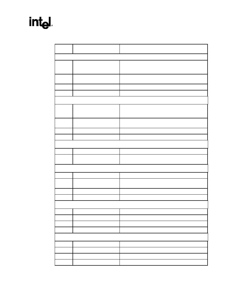
Electrical Characteristics
R
Intel
ģ
82845 MCH Datasheet 125
Table 20. Signal Groups
Signal
Group
Signal Type
Signals
Host Interface Signal Groups
(a)
AGTL+ I/O
ADS#, BNR#, BR0#,DBSY#, DBI[3:0]#,
DRDY#,
HA[31:3]#, HADSTB[1:0] #, HD[63:0]#,HDSTBP[3:0]#,
HDSTBN[3:0]#, HIT#, HITM#, HREQ[4:0]#
(b)
AGTL+ Common Clock
Output
BPRI#, CPURST#, DEFER#, HTRDY#, RS[2:0]#
(c)
AGTL+ Common Clock Input
HLOCK#
(d)
Host Reference Voltages
HVREF, HSWING[1:0]
AGP Interface Signal Groups
(e)
AGP I/O
AD_STB0, AD_STB0#, AD_STB1, AD_STB1#,
G_FRAME#, G_IRDY#, G_TRDY#, G_STOP#,
G_DEVSEL#, G_AD[31:0], G_CBE[3:0]#, G_PAR
(f)
AGP Input
PIPE#, SBA[7:0], RBF#, WBF#, SB_STB, SB_STB#,
G_REQ#
(g) AGP
Output
ST[2:0],
G_GNT#
(h)
AGP Reference Voltage
AGPREF
Hub Interface Signal Groups
(i)
Hub Interface's CMOS I/O
HI_[10:0], HI_STB, HI_STB#
(j)
Hub Interface Reference
Voltage
HI_REF
DDR Interface Signal Groups
(k)
DDR CMOS I/O
SDQ[63:0], SCB[7:0], SDQS[8:0]
(l)
DDR CMOS Output
SCS[3:0]#, SMA[12:0], SBS[1:0], SRAS#, SCAS#, SWE#,
SCKE[3:0], RCVENOUT#, SCK[5:0], SCK[5:0]#
(m)
DDR CMOS Input
RCVENIN#
(n)
DDR Reference Voltage
SDREF
Clocks, Reset, and Miscellaneous Signal Groups
(o) CMOS
Input
TESTIN#
(p)
CMOS Input
RSTIN# (3.3V)
(q)
CMOS Clock Input
BCLK, BCLK#
(v)
CMOS Clock Input
66IN
I/O Buffer Supply Voltages
(r)
AGTL+ Termination Voltage
VTT
(s)
1.5 V Core and AGP Voltage
VCC1_5
(t)
1.8 V Hub Interface Voltage
VCC1_8
(u)
2.5 V DDR Supply Voltage
VCCSM

Electrical Characteristics
R
126
Intel
ģ
82845 MCH Datasheet
6.4 DC
Characteristics
Table 21. DC Characteristics
Symbol Signal
Group
Parameter Min
Nom
Max
Unit
Notes
I/O Buffer Supply Voltage
VCCSM
(u)
DDR I/O Supply Voltage
2.375
2.5
2.625
V
VCC1_8
(t)
1.8V I/O Supply Voltage
1.71
1.8
1.89
V
VCC1_5
(s)
Core and AGP Voltage
1.425
1.5
1.575
V
VTT
(r)
Host AGTL+ Termination
Voltage
N/A N/A
1.75
V
Reference Voltages
HVREF
(d)
Host Address and Data
Reference Voltage
2/3 x VTT ≠ 2%
2/3 x VTT
2/3 x VTT + 2%
V
HSWING (d) Host
Compensation
Reference Voltage
1/3 x VTT ≠ 2%
1/3 x VTT
1/3 x VTT + 2%
V
HIREF
(j)
Hub Interface Reference
Voltage
0.48 x VCC1_8
1/2 x VCC1_8
0.52 x VCC1_8
V
SDREF
(n)
DDR Reference Voltage
0.48 x VCCSM
1/2 x VCCSM
0.52 x VCCSM
V
AGPREF
(h)
AGP Reference Voltage
0.48 x VCC1_5 1/2 x VCC1_5
0.52 x VCC1_5
V
Host Interface
V
IL_H
(a,c)
Host AGTL+ Input Low
Voltage
(2/3 x VTT) ≠ 0.1
V
V
IH_H
(a,c)
Host AGTL+ Input High
Voltage
(2/3 x VTT) + 0.1
V
V
OL_H
(a,b)
Host AGTL+ Output Low
Voltage
(1/3 x VTT) + 0.1
V
V
OH_H
(a,b)
Host AGTL+ Output High
Voltage
VTT≠0.1
V
I
OL_H
(a,b)
Host AGTL+ Output Low
Current
VTT
max
/ 0.75Rtt
min
mA Rtt
min
=45
I
LEAK_H
(a,c)
Host AGTL+ Input
Leakage Current
Ī
15
Ķ
A V
OL
<Vpad<
VTT
C
PAD
(a,c)
Host AGTL+ Input
Capacitance
1.0
pF

Electrical Characteristics
R
Intel
ģ
82845 MCH Datasheet 127
Symbol Signal
Group
Parameter Min
Nom
Max
Unit
Notes
DDR Interface
V
IL(DC)
(k,m)
DDR Input Low Voltage
SDREF
≠ 0.15
V
V
IH(DC)
(k,m)
DDR Input High Voltage
SDREF
+ 0.15
V
V
IL(AC)
(k,m)
DDR Input Low Voltage
SDREF
≠ 0.31
V
V
IH(AC)
(k,m)
DDR Input High Voltage
SDREF
+ 0.31
V
DDR Interface cont.
V
OL
(k,l)
DDR Output Low Voltage
0.975
V
1
V
OH
(k,l)
DDR Output High Voltage
1.80
V
1
I
OL
(k,l)
DDR Output Low Current
9.375
mA
1
I
OH
(k,l)
DDR Output High Current
-9.375
mA
1
I
Leak
(k,m)
Input Leakage Current
Ī
10 uA
C
I/O
(k, l, m) DDR Input/Output Pin
Capacitance
4.690 5.370
pF
1.5 V AGP Interface
V
IL_A
(e,f)
AGP Input Low Voltage
0.4 x VCC1_5
V
V
IH_A
(e,f)
AGP Input High Voltage
0.6 x VCC1_5
V
V
OL_A
(e,g)
AGP Output Low Voltage
0.15 x VCC1_5
V
V
OH_A
(e,g)
AGP Output High Voltage
0.85 x VCC1_5
V
I
OL_A
(e,g)
AGP Output Low Current
1
mA
@V
OL_A
max
I
OH_A
(e,g)
AGP Output High Current
-0.2
mA
@V
OH_A
max
I
LEAK_A
(e,f)
AGP Input Leakage
Current
Ī
15
Ķ
A 0<Vin<
VCC1_5
C
IN_A
(e,f)
AGP Input Capacitance
1.32
1.92
pF
1.8 V Hub Interface
V
IL_HI
(i)
Hub Interface Input Low
Voltage
HIREF ≠ 0.15
V
V
IH_HI
(i)
Hub Interface Input High
Voltage
HIREF + 0.15
V
V
OL_HI
(i)
Hub Interface Output Low
Voltage
0.1 x VCC1_8
V
I
OL
= 1 mA
V
OH_HI
(i)
Hub Interface Output High
Voltage
0.9 x VCC1_8
V
I
OH
= 1 mA
I
OL_HI
(i)
Hub Interface Output Low
Current
1
mA
@V
OL_HI
max
I
OH_HI
(i)
Hub Interface Output High
Current
-1
mA
@V
OH_HI
max

Electrical Characteristics
R
128
Intel
ģ
82845 MCH Datasheet
Symbol Signal
Group
Parameter Min
Nom
Max
Unit
Notes
I
LEAK_HI
(i)
Hub Interface Input
Leakage Current
-150,
+15
Ķ
A 0<Vin<
VCC1_8
C
IN_HI
(i)
Hub Interface Input
Capacitance
2.58 3.17
pF
Clocks, Reset, and Miscellaneous Signals
V
IL
(o)
Input Low Voltage
HIREF ≠ 0.15
V
V
IH
(o)
Input High Voltage
HIREF + 0.15
V
V
OL
(o)
Output Low Voltage
0.1 x VCC1_8
V
I
OL
= 1 mA
V
OH
(o)
Output High Voltage
0.9 x VCC1_8
V
I
OH
= 1 mA
I
OL
(o)
Output Low Current
1
mA
@V
OL_HI
max
I
OH
(o)
Output High Current
-1
mA
@V
OH_HI
max
I
LEAK
(o)
Input Leakage Current
≠150, +15
Ķ
A 0<Vin<VCC1_8
C
IN
(o)
Input
Capacitance 2.58 3.17
pF
V
IL
(p)
Input Low Voltage
0.8
V
V
IH
(p)
Input High Voltage
2.0
V
I
LEAK
(p)
Input Leakage Current
Ī
100
Ķ
A 0<Vin<VCC3_3
C
IN
(p)
Input
Capacitance 4.690 5.370
pF
V
IL
(q)
Input Low Voltage
0
V
V
IH
(q)
Input High Voltage
0.660
0.710
0.850
V
V
CROSS
(q)
Crossing
Voltage
0.45x(V
IH
≠ V
IL
) 0.5x(V
IH
≠ V
IL
) 0.55x(V
IH
≠ V
IL
) V
C
IN
(q)
Input
Capacitance
0.94
1.1
pF
V
IL
(v)
Input Low Voltage
0.8
V
V
IH
(v)
Input High Voltage
2.4
V
C
IN
(v)
Input
Capacitance 1.2 1.4
pF
NOTES:
1. Determined with 0.75x MCH DDR Buffer Strength Settings

Ballout and Package Information
R
Intel
ģ
82845 MCH Datasheet 129
7
Ballout and Package Information
This chapter provides the MCH ballout and package information. The ballout footprint is shown in
Figure 6 and Figure 7. These figures represent the ballout organized by ball number. Table 22
provides the MCH ballout listed alphabetically by signal name.
The following notes apply to the ballout.
Note: NC = No Connect.
Note: RSVD = These pins should not be connected and should be allowed to float.
Note: VSS = Connect to ground.
Ballout and Package Information
R
130
Intel
ģ
82845 MCH Datasheet
Figure 6. Intel
ģ
82845 MCH Ballout Diagram (Top View--Left Side)
29 28 27 26 25 24 23 22 21 20 19
18 17 16 15
AJ
VSS
VCC1_5 VTT VTT
VTT
VSS VSS
AH
SBA0
SBA1
G_GNT# VSS VSS
VSS
HD61#
HD57#
AG
VCC1_5
SBA2 SBA3 ST2 ST0 G_REQ# VTT VSS VTT VSS
VTT
VSS
HD56#
HD55#
HD54#
AF
SB_STB
SB_STB#
VSS
ST1 VCC1_5
PIPE# VSS VTT VSS
VTT VSS HD59# VSS
AE
VSS SBA4 SBA5
VCC1_5
SBA7 SBA6 WBF#
RBF# VTT VSS
VTT
VSS
CPURST#
HD63#
HD60#
AD
NC
NC GRCOMP
G_AD31
VCC1_5 VSS VCC1_5 VTT VSS
VTT HD62# VSS DBI3#
AC
VCC1_5
AD_STB1#
AD_STB1 VSS G_AD28 G_AD29 VSS G_AD30 VSS VSS VTT VSS HD58#
HDSTBP3#
HDSTBN
3#
AB
G_AD20 G_AD22
G_AD19 G_AD27 G_AD24 VSS VCC1_5 VTT VSS VTT HVREF VSS VSS
AA
VSS G_AD18 G_AD21 VCC1_5
G_AD26 G_AD25 G_CBE3#
VCC1_5
AGPREF
Y
G_AD16
G_AD17
G_CBE2#
G_FRAME#
G_AD23
VSS
W
VCC1_5
G_DEVSEL#
G_IRDY#
VSS
G_PAR
G_TRDY#
G_STOP#
VCC1_5
V
G_AD9 G_AD8 G_CBE0# G_AD15 G_CBE1# VSS
U
VSS G_AD7 G_AD6 VCC1_5
G_AD14 G_AD13 G_AD11 VCC1_5
VSSA1 VCC1_5 VSS
T
G_AD5
G_AD4
G_AD2
G_AD12
G_AD10
VSS
VCCA1
VSS
VCC1_5
R
VCC1_5 G_AD1 G_AD0
VSS G_AD3 AD_STB0 AD_STB0#
VCC1_5
VSS VCC1_5 VSS
P
HLRCOMP
HI_REF
HI_0
HI_1
HI_3
66IN
VCC1_5
VSS
VCC1_5
N
VSS HI_9 HI_2
VCC1_8
HI_STB
HI_STB#
VCC1_8
VSS
VSS
VCC1_5
VSS
M
HI_8
HI_4
HI_5
HI_10
VSS
VCC1_8
L
VCC1_8
HI_6
HI_7
VSS
VCC1_8
VSS
VCCSM
VSS
K
VSS
VCCSM
RSVD
VCCSM
RSVD
VCCSM
J
VSS
SMRCOMP
RSTIN# VSS RSVD SCK1 RSVD VSS SDREF
H
RSVD TESTIN# SDQ4 VCCSM SCKE2 VCCSM VSS VCCSM VSS VCCSM VSS VCCSM VSS
G
VCCSM SDQ0
SDQ5 VSS SCK#1 SCK#4 SCKE0 SMA12 SMA7 SMA8 SMA4
SMA3 RSVD RSVD SCK3
F
SDQ1 SDQS0
SDQ6 VSS SCKE3
VCCSM
SMA9 VSS
SMA6
VCCSM
SMA1 VSS
SCK#0
E
VSS SDQ3 SDQ8 VSS SDQ15 SCK4 SDQ17
SCKE1
SDQ19
SMA11
SDQ29
SMA5
SDQ31
SMA2
SDQS8
D
SDQ13 SDQ14
VCCSM SDQ16 VCCSM
SDQ22 VSS SDQ25
VCCSM
SDQ27 VSS SCB1
VCCSM
C
VCCSM SDQ2
SDQ9 SDQS1 SDQ11 SDQ20 SDQS2 SDQ18 SDQ24 SDQ28 SDQ26
SDQ30 SCB5 SCB0 SCB6
B
SDQ7
SDQ12 SDQ10 SDQ21 SDQ23
SDQS3
SCB4 SCB2
A
VSS
VCCSM
VSS
VCCSM
VSS
VCCSM
VSS
29 28 27 26 25 24 23 22 21 20 19
18 17 16 15
NOTES:
1.
NC = No Connect.
2.
RSVD = These pins should not be connected and should be allowed to float.
3.
VSS = Connect to ground.
Ballout and Package Information
R
Intel
ģ
82845 MCH Datasheet 131
Figure 7. Intel
ģ
82845 MCH Ballout Diagram (Top View--Right Side)
14 13 12 11 10 9 8 7 6 5 4 3 2 1
VSS VSS VSS VSS VSS VSS
AJ
HD49# HD44# DBI2# HD24# HD31# HD25#
HD20#
AH
HD52# HD48# HD45# HD42# HD43# HD38# HD27# HD28# HD29# HD16# DBI1# HD22# HD17# VSS
AG
HD51# VSS HD47# VSS HD41# VSS HD30# VSS HD19# VSS HD26# HD21#
AF
HD53# HD46# HD40# HDSTBN2#
HD36# HD34# HD18# HDSTBP1#
HDSTBN1# HD23#
VSS
HD8#
HD15#
VSS
AE
VSS
HSWNG1
VSS
HDSTBP2#
VSS HD37# VSS HD10# VSS DBI0#
HDSTBN0#
HDSTBP0#
AD
HD50#
HRCOMP1
HD33# HD32# HD39# HD35# HD14# HD11# HD12# HD5# VSS HD13#
HRCOMP0 VSS
AC
VSS VSS VSS
HVREF
VSS VSS VTT HD9# VSS HD1# HD4# HD3#
AB
VTT
VSS
HSWNG0
HD7#
HD2#
VSS
HD6#
HD0#
VSS
AA
HVREF
BPRI#
VSS
HIT#
DEFER#
HITM#
Y
VSS
RS1#
RS2#
HLOCK#
VSS
BNR#
RS0#
VSS
W
VSS
BR0#
VSS
DBSY#
DRDY#
ADS#
V
VCC1_5 VSSA0
VTT HTRDY#
HREQ0#
HREQ3# VSS HA6# HREQ4# VSS
U
VSS VCCA0
VSS HREQ1# VSS HA4# HA3# HA5#
T
VCC1_5 VSS
HVREF
HREQ2#
HA11#
HADSTB0#
VSS HA7# HA9# VSS
R
VSS
VCC1_5
VSS
HA8#
VSS
HA12#
HA10#
HA13#
P
VCC1_5 VSS
VSS HA15#
HADSTB1#
HA28# VSS HA16# HA14# VSS
N
VTT
HVREF
HA30#
HA24#
HA18#
HA19#
M
VSS HA31# VSS HA21# VSS HA20# HA26# VSS
L
BCLK#
VSS
VCCSM
VSS
HA17#
HA22#
K
SDREF BCLK VCCSM VSS VCCSM VSS HA25# HA23# VSS
J
VCCSM VSS VCCSM VSS VCCSM VSS VCCSM RSVD RSVD SCK5 HA27#
RCVENOUT
#
H
SCK#3 SBS1 SBS0 SWE# RSVD RSVD SCAS# SCK#2 SCK2 SDQ63
VCCSM
RCVENIN#
HA29# VCCSM
G
VCCSM SMA10 VSS SRAS# VCCSM SCS#2 VSS SCS#1 VCCSM SCK#5 SDQ58 SDQ59
F
SCK0 SDQ32 SMA0 SDQ44 SDQ40 SCS#0 SDQ43 SCS#3 SDQ52 SDQ55 VSS SDQS7 SDQ62 VSS
E
SCB7
VSS SDQS4 VCCSM SDQ39 VSS SDQ42 VCCSM SDQ49 VSS SDQ50 SDQ57
D
SCB3 SDQ37 SDQ33 SDQ38 SDQ35 SDQ41 SDQS5 SDQ47 SDQ48 SDQS6 SDQ54 SDQ56 SDQ61 VCCSM
C
SDQ36 SDQ34 SDQ45 SDQ46 SDQ53 SDQ51
SDQ60
B
VCCSM VSS VCCSM VSS VCCSM VSS
A
14 13 12 11 10 9 8 7 6 5 4 3 2 1
NOTES:
1.
NC = No Connect.
2.
RSVD = These pins should not be connected and should be allowed to float.
3.
VSS = Connect to ground.
Ballout and Package Information
R
132
Intel
ģ
82845 MCH Datasheet
Table 22. Intel
ģ
82845 MCH Ballout Listed Alphabetically by Signal Name
Signal Name
Ball #
66IN P22
AD_STB0 R24
AD_STB0# R23
AD_STB1 AC27
AD_STB1# AC28
ADS# V3
AGPREF AA21
BCLK# K8
BCLK J8
BNR# W3
BPRI# Y7
BR0# V7
CPURST# AE17
DBSY# V5
DEFER# Y4
DBI0# AD5
DBI1# AG4
DBI2# AH9
DBI3# AD15
DRDY# V4
G_AD0 R27
G_AD1 R28
G_AD2 T25
G_AD3 R25
G_AD4 T26
G_AD5 T27
G_AD6 U27
G_AD7 U28
G_AD8 V26
G_AD9 V27
G_AD10 T23
G_AD11 U23
G_AD12 T24
G_AD13 U24
Signal Name
Ball #
G_AD14 U25
G_AD15 V24
G_AD16 Y27
G_AD17 Y26
G_AD18 AA28
G_AD19 AB25
G_AD20 AB27
G_AD21 AA27
G_AD22 AB26
G_AD23 Y23
G_AD24 AB23
G_AD25 AA24
G_AD26 AA25
G_AD27 AB24
G_AD28 AC25
G_AD29 AC24
G_AD30 AC22
G_AD31 AD24
G_CBE0# V25
G_CBE1# V23
G_CBE2# Y25
G_CBE3# AA23
G_DEVSEL# W28
G_FRAME# Y24
G_GNT# AH25
G_IRDY# W27
G_PAR W25
G_REQ# AG24
G_STOP# W23
G_TRDY# W24
GRCOMP AD25
HA3# T4
HA4# T5
HA5# T3

Ballout and Package Information
R
Intel
ģ
82845 MCH Datasheet 133
Signal Name
Ball #
HA6# U3
HA7# R3
HA8# P7
HA9# R2
HA10# P4
HA11# R6
HA12# P5
HA13# P3
HA14# N2
HA15# N7
HA16# N3
HA17# K4
HA18# M4
HA19# M3
HA20# L3
HA21# L5
HA22# K3
HA23# J2
HA24# M5
HA25# J3
HA26# L2
HA27# H4
HA28# N5
HA29# G2
HA30# M6
HA31# L7
HADSTB0# R5
HADSTB1# N6
HD0# AA2
HD1# AB5
HD2# AA5
HD3# AB3
HD4# AB4
HD5# AC5
HD6# AA3
HD7# AA6
Signal Name
Ball #
HD8# AE3
HD9# AB7
HD10# AD7
HD11# AC7
HD12# AC6
HD13# AC3
HD14# AC8
HD15# AE2
HD16# AG5
HD17# AG2
HD18# AE8
HD19# AF6
HD20# AH2
HD21# AF3
HD22# AG3
HD23# AE5
HD24# AH7
HD25# AH3
HD26# AF4
HD27# AG8
HD28# AG7
HD29# AG6
HD30# AF8
HD31# AH5
HD32# AC11
HD33# AC12
HD34# AE9
HD35# AC9
HD36# AE10
HD37# AD9
HD38# AG9
HD39# AC10
HD40# AE12
HD41# AF10
HD42# AG11
HD43# AG10

Ballout and Package Information
R
134
Intel
ģ
82845 MCH Datasheet
Signal Name
Ball #
HD44# AH11
HD45# AG12
HD46# AE13
HD47# AF12
HD48# AG13
HD49# AH13
HD50# AC14
HD51# AF14
HD52# AG14
HD53# AE14
HD54# AG15
HD55# AG16
HD56# AG17
HD57# AH15
HD58# AC17
HD59# AF16
HD60# AE15
HD61# AH17
HD62# AD17
HD63# AE16
HDSTBN0# AD4
HDSTBP0# AD3
HDSTBN1# AE6
HDSTBP1# AE7
HDSTBN2# AE11
HDSTBP2# AD11
HDSTBN3# AC15
HDSTBP3# AC16
HI_0 P25
HI_1 P24
HI_2 N27
HI_3 P23
HI_4 M26
HI_5 M25
HI_6 L28
HI_7 L27
Signal Name
Ball #
HI_8 M27
HI_9 N28
HI_10 M24
HI_REF P26
HI_STB N25
HI_STB# N24
HIT# Y5
HITM# Y3
HLOCK# W5
HLRCOMP P27
HRCOMP0 AC2
HRCOMP1 AC13
HREQ0# U6
HREQ1# T7
HREQ2# R7
HREQ3# U5
HREQ4# U2
HSWNG0 AA7
HSWNG1 AD13
HTRDY# U7
HVREF M7,R8,Y8,AB11,
AB17
NC AD26,AD27
PIPE# AF22
RBF# AE22
RCVENIN# G3
RCVENOUT# H3
RS0# W2
RS1# W7
RS2# W6
RSTIN# J27
RSVD G9,G10,G16,G17,H6,H7,H27J2
3,J25,K23,K25
SBA0 AH28
SBA1 AH27
SBA2 AG28
SBA3 AG27

Ballout and Package Information
R
Intel
ģ
82845 MCH Datasheet 135
Signal Name
Ball #
SBA4 AE28
SBA5 AE27
SBA6 AE24
SBA7 AE25
SB_STB AF27
SB_STB# AF26
SCAS# G8
SCK0 E14
SCK1 J24
SCK2 G6
SCK3 G15
SCK4 E24
SCK5 H5
SBS0 G12
SBS1 G13
SCK#0 F15
SCK#1 G25
SCK#2 G7
SCK#3 G14
SCK#4 G24
SCK#5 F5
SCKE0 G23
SCKE1 E22
SCKE2 H23
SCKE3 F23
SCS#0 E9
SCS#1 F7
SCS#2 F9
SCS#3 E7
SDQ0 G28
SDQ1 F27
SDQ2 C28
SDQ3 E28
SDQ4 H25
SDQ5 G27
SDQ6 F25
Signal Name
Ball #
SDQ7 B28
SDQ8 E27
SDQ9 C27
SDQ10 B25
SDQ11 C25
SDQ12 B27
SDQ13 D27
SDQ14 D26
SDQ15 E25
SDQ16 D24
SDQ17 E23
SDQ18 C22
SDQ19 E21
SDQ20 C24
SDQ21 B23
SDQ22 D22
SDQ23 B21
SDQ24 C21
SDQ25 D20
SDQ26 C19
SDQ27 D18
SDQ28 C20
SDQ29 E19
SDQ30 C18
SDQ31 E17
SDQ32 E13
SDQ33 C12
SDQ34 B11
SDQ35 C10
SDQ36 B13
SDQ37 C13
SDQ38 C11
SDQ39 D10
SDQ40 E10
SDQ41 C9
SDQ42 D8
Ballout and Package Information
R
136
Intel
ģ
82845 MCH Datasheet
Signal Name
Ball #
SDQ43 E8
SDQ44 E11
SDQ45 B9
SDQ46 B7
SDQ47 C7
SDQ48 C6
SDQ49 D6
SDQ50 D4
SDQ51 B3
SDQ52 E6
SDQ53 B5
SDQ54 C4
SDQ55 E5
SDQ56 C3
SDQ57 D3
SDQ58 F4
SDQ59 F3
SDQ60 B2
SDQ61 C2
SDQ62 E2
SDQ63 G5
SCB0 C16
SCB1 D16
SCB2 B15
SCB3 C14
SCB4 B17
SCB5 C17
SCB6 C15
SCB7 D14
SDQS0 F26
SDQS1 C26
SDQS2 C23
SDQS3 B19
SDQS4 D12
SDQS5 C8
SDQS6 C5
Signal Name
Ball #
SDQS7 E3
SDQS8 E15
SDREF J9,
J21
SMA0 E12
SMA1 F17
SMA2 E16
SMA3 G18
SMA4 G19
SMA5 E18
SMA6 F19
SMA7 G21
SMA8 G20
SMA9 F21
SMA10 F13
SMA11 E20
SMA12 G22
SMRCOMP J28
SRAS# F11
ST0 AG25
ST1 AF24
ST2 AG26
SWE# G11
TESTIN# H26
VCC1_5
R22, R29, U22, U26, W22,
W29, AA22, AA26, AB21,
AC29, AD21, AD23, AE26,
AF23, AG29, AJ25
VCC1_5
N14, N16, P13, P15, P17, R14,
R16, T15, U14, U16
VCC1_5 T17
VCC1_5 T13
VCC1_8
L25, L29, M22, N23, N26
VCCSM
A5, A9, A13, A17, A21, A25,
C1, C29, D7, D11, D15, D19,
D23, D25, F6, F10, F14, F18,
F22, G1, G4, G29, H8, H10,
H12, H14, H16, H18, H20, H22,
H24, J5, J7, K6, K22, K24,
K26, L23

Ballout and Package Information
R
Intel
ģ
82845 MCH Datasheet 137
Signal Name
Ball #
VSS
A3, A7, A11, A15, A19, A23,
A27, D5, D9, D13, D17, D21,
E1, E4, E26, E29, F8, F12,
F16, F20, F24, G26, H9, H11,
H13, H15, H17, H19, H21, J1,
J4, J6, J22, J26, J29, K5, K7,
K27, L1, L4, L6, L8, L22, L24,
L26, M23, N1, N4, N8, N13,
N15, N17, N22, N29, P6, P8,
P14, P16, R1, R4, R13, R15,
R17, R26, T6, T8, T14, T16,
T22, U1, U4, U15, U29, V6, V8,
V22, W1, W4, W8, W26, Y6,
Y22, AA1, AA4, AA8, AA29,
AB6, AB9, AB10, AB12, AB13,
AB14, AB15, AB16, AB19,
AB22, AC1, AC4, AC18, AC20,
AC21, AC23, AC26, AD6, AD8,
AD10, AD12, AD14, AD16,
AD19, AD22, AE1, AE4, AE18,
AE20, AE29, AF5, AF7, AF9,
AF11, AF13, AF15, AF17,
AF19, AF21, AF25, AG1,
AG18, AG20, AG22, AH19,
AH21, AH23, AJ3, AJ5, AJ7,
AJ9, AJ11, AJ13, AJ15, AJ17,
AJ27
Signal Name
Ball #
VSSA U17
VSS U13
VTT
M8, U8, AA9, AB8, AB18,
AB20, AC19, AD18, AD20,
AE19, AE21, AF18, AF20,
AG19, AG21, AG23, AJ19,
AJ21, AJ23
WBF# AE23
NOTES:
1. NC = No Connect.
2. RSVD = These pins should not be connected
and should be allowed float.
3. VSS = Connect to ground.
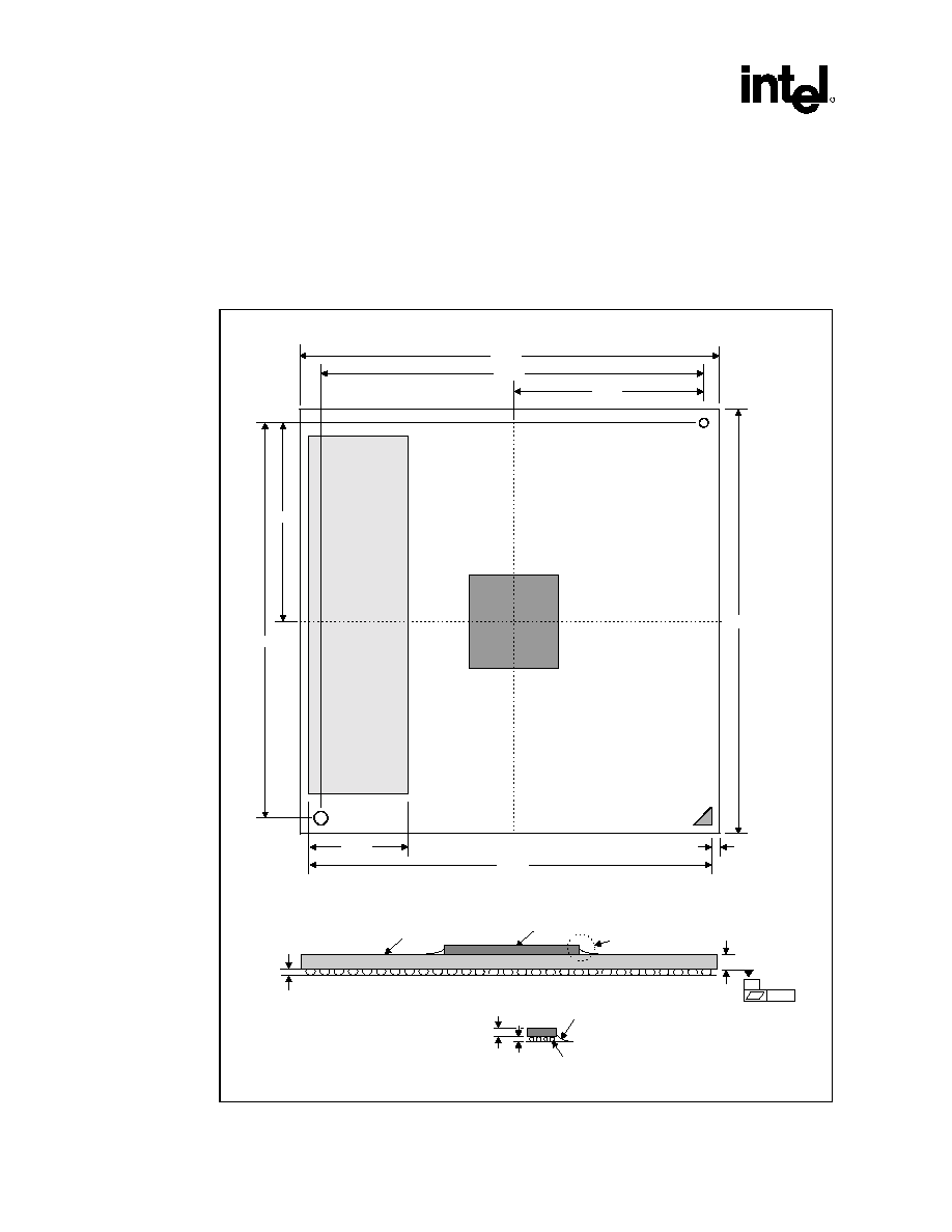
Ballout and Package Information
R
138
Intel
ģ
82845 MCH Datasheet
7.1
Package Mechanical Information
This section provides the MCH package mechanical dimensions. The package is a 593-ball
FC-BGA.
Figure 8. Intel
ģ
82845 MCH FC-BGA Package Dimensions (Top and Side View)
pkg_olga_593_top-side
Units = M illim eters
9.67
36.28
33.90
Top View
0.61
16.95
16.95
33.90
37.50
37.50
1.100 Ī0.100
Die
0.152
A
Side View
Substrate
0.600 Ī0.100
See Detail A
Detail A
0.74 Ī0.025
0.10 Ī0.025
Die Solder
Bum ps
Underfill
Epoxy

Ballout and Package Information
R
Intel
ģ
82845 MCH Datasheet 139
Figure 9. Intel
ģ
82845 MCH FC-BGA Package Dimensions (Bottom View)
pkg-MCH_olga_593_Bot
D
E
G
H
K
L
P
R
U
V
Y
N
W
M
AA
AB
AC
AD
AE
AF
J
F
A
AH
AG
AJ
1.270
B
C
T
10
16
20
3
5
7
9
11
13
15
17
19
4
6
18
8
12
14
22
21
24
23
26
25
28
27
29
1
2
17.780
35.560
1.270
17.780
35.560
Note: All dim ensions are in m illim eters

Ballout and Package Information
R
140
Intel
ģ
82845 MCH Datasheet
This page is intentionally left blank.
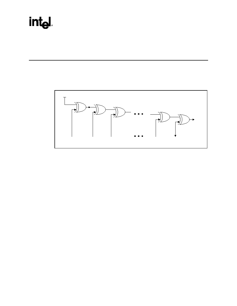
Testability
R
Intel
ģ
82845 MCH Datasheet 141
8 Testability
In the MCH, testability for Automated Test Equipment (ATE) board-level testing has been
implemented as an XOR chain. An XOR-tree is a chain of XOR gates, each with one input pin
connected to it (see Figure 10).
Figure 10. XOR Tree Chain
Input
XOR
Out
xor.vsd
Input
Input
Input
Input
VCC1_8
The algorithm used for in-circuit test is as follows:
∑
Drive all input pins to an initial logic level 1. Observe the output corresponding to scan chain
being tested.
∑
Toggle pins one at a time (starting from the first pin in the chain and continuing to the last
pin) from its initial logic level to the opposite logic level. Observe the ou
t
put changes with
each pin toggle.
8.1
XOR Test Mode Initialization
XOR test mode can be entered by pulling three shared pins (reset straps) low through the rising
transition of RSTIN#. The signals that need to be pulled are as follows:
∑
G_GNT# = 0 (Global strap enable)
∑
SBA1 = 0 (XOR strap)
∑
ST2 = 0 (PLL Bypass mode; it is recommended to enter PLL Bypass in XOR test mode)

Testability
R
142
Intel
ģ
82845 MCH Datasheet
8.2 XOR
Chains
Note: RSTIN#, TESTIN#, and all Rcomp buffers are not part of any XOR chain.
Table 23. XOR Chain 0
Chain O Ball
Element #
Signal Name
Note
Initial Logic Level
AE6 1
HDSTBP1#
Input 1
AD3 2
HDSTBP0#
Input 1
V3 3 ADS#
Input 1
U6 4 HREQ0#
Input 1
U3 5 HA6#
Input 1
U2 6 HREQ4#
Input 1
U5 7 HREQ3#
Input 1
T5 8 HA4#
Input 1
T7 9 HREQ1#
Input 1
T4 10 HA3#
Input 1
R7 11 HREQ2#
Input 1
R5 12
HADSTB0#
Input 1
R3 13 HA7#
Input 1
P3 14 HA13#
Input 1
R2 15 HA9#
Input 1
R6 16 HA11#
Input 1
T3 17 HA5#
Input 1
N3 18 HA16#
Input 1
P5 19 HA12#
Input 1
P4 20 HA10#
Input 1
P7 21 HA8#
Input 1
N2 23 HA14#
Input 1
N7 24 HA15#
Input 1
N5 25 HA28#
Input 1
M4 26 HA18#
Input 1
L3 27 HA20#
Input 1
M3 28 HA19#
Input 1
L2 29 HA26#
Input 1
K3 30 HA22#
Input 1
M5 31 HA24#
Input 1
K3 32 HA23#
Input 1
K4 33 HA17#
Input 1
J3 34 HA25#
Input 1
L5 35 HA21#
Input 1

Testability
R
Intel
ģ
82845 MCH Datasheet 143
Chain O Ball
Element #
Signal Name
Note
Initial Logic Level
H4 36 HA27#
Input 1
M6 37 HA30#
Input 1
L7 38 HA31#
Input 1
G2 39 HA29#
Input 1
H6 40 RSVD
Input 1
H3 41
RCVENOUT#
Input 1
G3 42
RCVENIN#
Input 1
H5 43 SCK5
Input 1
G6 44 SCK2
Input 1
E7 45 SCS3#
Input 1
G8 46 SCAS#
Input 1
G9 47 RSVD
Input 1
AH28 48 SBA0 Output N/A

Testability
R
144
Intel
ģ
82845 MCH Datasheet
Table 24. XOR Chain 1
Chain 1 Ball
Element #
Signal Name
Note
Initial Logic Level
N6 1
HADSTB1#
Input 1
H7 2 SCK5#
Input 1
G10 3 RSVD
Input 1
G5 4 SDQ63
Input 1
F4 5 SDQ58
Input 1
F3 6 SDQ59
Input 1
C2 7 SDQ61
Input 1
B2 8 SDQ60
Input 1
E2 9 SDQ62
Input 1
D3 10 SDQ57
Input 1
E3 11 SDQS7
Input 1
G7 12 SCK2#
Input 1
C3 13 SDQ56
Input 1
E5 14 SDQ55
Input 1
F7 15 SCS1#
Input 1
D4 16 SDQ50
Input 1
C4 17 SDQ54
Input 1
C5 18 SDQS6
Input 1
E6 19 SDQ52
Input 1
D6 20 SDQ49
Input 1
B3 21 SDQ51
Input 1
C6 22 SDQ48
Input 1
B5 23 SDQ53
Input 1
C7 24 SDQ47
Input 1
B7 25 SDQ46
Input 1
E8 26 SDQ43
Input 1
C8 27 SDQ35
Input 1
C9 28 SDQ41
Input 1
D8 29 SDQ42
Input 1
E10 30 SDQ40
Input 1
B9 31 SDQ45
Input 1
E11 32 SDQ44
Input 1
E9 33 SCS0#
Input 1
AH27 34 SBA1
Output N/A

Testability
R
Intel
ģ
82845 MCH Datasheet 145
Table 25. XOR Chain 2
Chain 2 Ball
Element #
Signal Name
Note
Initial Logic Level
D10 1 SDQ39
Input 1
C10 2 SDQ35
Input 1
C11 3 SDQ38
Input 1
F9 4 SCS2#
Input 1
B11 5 SDQ34
Input 1
B13 6 SDQ36
Input 1
G11 7 SWE#
Input 1
C12 8 SDQ33
Input 1
F11 9 SRAS#
Input 1
C13 10 SDQ37
Input 1
D12 11 SDQS4
Input 1
E12 12 SMA0
Input 1
E13 13 SDQ32
Input 1
G14 14 SCK3#
Input 1
G13 15 SBS1
Input 1
F15 16 SCK0#
Input 1
E15 17 SDQS8
Input 1
G16 18 RSVD
Input 1
E16 19 SMA2
Input 1
E18 20 SMA5
Input 1
F17 21 SMA1
Input 1
F19 22 SMA6
Input 1
G18 23 SMA3
Input 1
G20 24 SMA8
Input 1
G19 25 SMA4
Input 1
F21 26 SMA9
Input 1
G21 27 SMA7
Input 1
E22 28 SCKE1
Input 1
G24 29 SCK4#
Input 1
G23 30 SCKE0
Input 1
G25 31 SCK1#
Input 1
H23 32 SCKE2
Input 1
J25 33 RSVD
Input 1
AG28 34 SBA2
Output N/A

Testability
R
146
Intel
ģ
82845 MCH Datasheet
Table 26. XOR Chain 3
Chain 3
Ball
Element #
Ball Name
Note
Initial Logic
Level
G10 1 RSVD
Input 1
G12 2 SBS0
Input 1
G15 3 SCK3
Input 1
F13 4 SMA10
Input 1
C14 5 SCB3
Input 1
E14 6 SCK0
Input 1
D14 7 SCB7
Input 1
C15 8 SCB6
Input 1
G17 9 RSVD
Input 1
C16 10 SCB0 Input 1
D16 11 SCB1 Input 1
B15 12 SCB2 Input 1
C17 13 SCB5 Input 1
B17 14 SCB4 Input 1
D18 15 SDQ27
Input 1
E17 16 SDQ31
Input 1
B19 17 SDQS3
Input 1
C18 18 SDQ30
Input 1
E19 19 SDQ29
Input 1
C19 20 SDQ26
Input 1
C20 21 SDQ28
Input 1
D20 22 SDQ25
Input 1
C21 23 SDQ24
Input 1
E20 24 SMA11
Input 1
B21 25 SDQ23
Input 1
E21 26 SDQ19
Input 1
C22 27 SDQ18
Input 1
D22 28 SDQ22
Input 1
C24 29 SDQ20
Input 1
C23 30 SDQS2
Input 1
B23 31 SDQ21
Input 1
D24 32 SDQ16
Input 1
G22 33 SMA12
Input 1
E23 34 SDQ17
Input 1
B25 35 SDQ10
Input 1
C25 36 SDQ11
Input 1
C27 37 SDQ9 Input 1
D27 38 SDQ13
Input 1
B27 39 SDQ12
Input 1
Testability
R
Intel
ģ
82845 MCH Datasheet 147
Chain 3
Ball
Element #
Ball Name
Note
Initial Logic
Level
C26 40 SDQS1
Input 1
F23 41 SCKE3
Input 1
E24 42 SCK4 Input 1
E25 43 SDQ15
Input 1
E27 44 SDQ8 Input 1
N24 45 HI_STB#
Input 1
R24 46 AD_STB0
Input 1
AG27 47
SBA3 Output N/A
Table 27. XOR Chain 4
Chain 4
Ball
Element #
DDR Ball Name
Note
Initial Logic
Level
D26 1 SDQ14
Input 1
F25 2 SDQ6
Input 1
B28 3 SDQ7
Input 1
C28 4 SDQ2
Input 1
E28 5 SDQ3
Input 1
J24 6 SCK1
Input 1
F26 7 SDQS0
Input 1
H25 8 SDQ4
Input 1
K25 9 RSVD
Input 1
J23 10 RSVD
Input 1
F27 11 SDQ1 Input 1
K23 12 RSVD Input 1
G28 13 SDQ0 Input 1
G27 14 SDQ5 Input 1
M27 15
RQM Input 1
M24 16 PSTOP
Input 1
N28 17
RQI Input 1
L28 18
HI_6 Input 1
M25 19
HI_5 Input 1
N27 20
HI_2 Input 1
M26 21
HI_4 Input 1
N25 22 HI_STB
Input 1
L27 23
HI_7 Input 1
P25 24
HI_0 Input 1
P23 25
HI_3 Input 1
P24 26
HI_1 Input 1
R27 27 G_AD0
Input 1
R28 28 G_AD1
Input 1

Testability
R
148
Intel
ģ
82845 MCH Datasheet
Chain 4
Ball
Element #
DDR Ball Name
Note
Initial Logic
Level
U27 29 G_AD6
Input 1
R25 30 G_AD3
Input 1
T27 31 G_AD5
Input 1
T36 32 G_AD4
Input 1
U28 33 G_AD7
Input 1
R24 34 AD_STB0
Input 1
V27 35 G_AD9
Input 1
T25 36 G_AD2
Input 1
U27 37 G_AD8
Input 1
T24 38 G_AD12
Input 1
U24 39 G_AD13
Input 1
U25 40 G_AD14
Input 1
T23 41 G_AD10
Input 1
V24 42 G_AD15
Input 1
U23 43 G_AD11
Input 1
AE28 44
SBA4 Output N/A

Testability
R
Intel
ģ
82845 MCH Datasheet 149
Table 28. XOR Chain 5
Chain 5
Ball
Element #
DDR Ball Name
Note
Initial Logic
Level
V25 1 G_C/BE0#
Input 1
W28 2 G_DEVSEL#
Input 1
W25 3 G_PAR
Input 1
Y25 4 G_C/BE2#
Input 1
W27 5 G_IRDY#
Input 1
V23 6 G_C/BE1#
Input 1
Y24 7 G_FRAME#
Input 1
W24 8 G_TRDY#
Input 1
AE23 9
WBF# Input 1
W23 10 G_STOP#
Input 1
AA23 11 G_C/BE3#
Input 1
AA28 12 G_AD18
Input 1
Y26 13 G_AD17
Input 1
Y27 14 G_AD16
Input 1
AB27 15 G_AD20
Input 1
AB26 16 G_AD22
Input 1
AA25 17 G_AD26
Input 1
AA24 18 G_AD25
Input 1
AA27 19 G_AD21
Input 1
AC27 20 AD_STB1
Input 1
Y23 21 G_AD23
Input 1
AC25 22 G_AD28
Input 1
AB25 23 G_AD19
Input 1
AB23 24 G_AD24
Input 1
AB24 25 G_AD31
Input 1
AC24 26 G_AD29
Input 1
AC22 27 G_AD30
Input 1
AB24 28 G_AD27
Input 1
AE22 29
RBF# Input 1
AF24 30
ST1 Input 1
AF22 31
PIPE# Input 1
AF27 32 SB_STB
Input 1
AH25 33 G_GNT#
Input 1
AG25 34
ST0 Input 1
AG24 35 G_REQ#
Input 1
AG26 36
ST2 Input 1
AH17 37 HD61# Input 1
AG16 38 HD55# Input 1

Testability
R
150
Intel
ģ
82845 MCH Datasheet
Chain 5
Ball
Element #
DDR Ball Name
Note
Initial Logic
Level
AG17 39 HD56# Input 1
AC16 40 HDSTBP3#
Input 1
AE11 41 HDSTBP2#
Input 1
AE27 42
SBA5 Output N/A
Table 29. XOR Chain 6
Chain 6
Ball
Element #
DDR Ball Name
Note
Initial Logic
Level
AC27 1 AD_STB1
Input 1
AF27 2 SB_STB
Input 1
AE17 3 CPURST#
Input 1
AD17 4 HD62#
Input 1
AE16 5 HD63#
Input 1
AH15 6 HD57#
Input 1
AG15 7
HD54# Input 1
AF16 8 HD59#
Input 1
AC16 9 HDSTBN3#
Input 1
AE15 10 HD60# Input 1
AG14 11 HD52# Input 1
AC17 12 HD58# Input 1
AF14 13 HD51# Input 1
AE14 14 HD53# Input 1
AH13 15 HD49# Input 1
AD15 16
DBI3# Input 1
AG13 17 HD48# Input 1
AC14 18 HD50# Input 1
AF12 19 HD47# Input 1
AG12 20 HD45# Input 1
AE12 21 HD40# Input 1
AE13 22 HD46# Input 1
AH9 23 DBI2# Input 1
AG10 24 HD43# Input 1
AH11 25 HD44# Input 1
AG9 26 HD38# Input 1
AG11 27 HD42# Input 1
AE11 28 HDSTBN2#
Input 1
AF10 29 HD41# Input 1
AE10 30 HD36# Input 1
AC12 31 HD33# Input 1
AC11 32 HD32# Input 1

Testability
R
Intel
ģ
82845 MCH Datasheet 151
Chain 6
Ball
Element #
DDR Ball Name
Note
Initial Logic
Level
AC10 33 HD39# Input 1
AE9 34 HD34#
Input 1
AC9 35 HD35#
Input 1
AD9 36 HD37#
Input 1
AH7 37 HD24#
Input 1
AH5 38 HD31#
Input 1
AG8 39 HD27# Input 1
Y4 40 DEFER#
Input 1
W7 41 RS1# Input 1
AE24 42
SBA6 Output N/A
Table 30. XOR Chain 7
Chain 7
Ball
Element #
Ball Name
Note
Initial Logic
Level
AG6 1 HD29# Input 1
AG5 2 HD16# Input 1
AG7 3 HD28# Input 1
AF6 4 HD19#
Input 1
AF8 5 HD30#
Input 1
AE6 6 HDSTBN1#
Input 1
AG4 7 DBI1# Input 1
AH3 8 HD25# Input 1
AE8 9 HD18#
Input 1
AG2 10 HD17# Input 1
AF4 11 HD26# Input 1
AH2 12 HD20# Input 1
AE5 13 HD23# Input 1
AG3 14 HD22# Input 1
AF3 15 HD21# Input 1
AD7 16 HD10# Input 1
AC7 17 HD11# Input 1
AC8 18 HD14# Input 1
AD5 19 DBI0# Input 1
AC6 20 HD12# Input 1
AE2 21 HD15# Input 1
AB7 22 HD9# Input 1
AE3 23 HD8# Input 1
AD4 24 HDSTBN0#
Input 1
AC3 25 HD13# Input 1
AB5 26 HD1# Input 1

Testability
R
152
Intel
ģ
82845 MCH Datasheet
Chain 7
Ball
Element #
Ball Name
Note
Initial Logic
Level
AC5 27 HD5# Input 1
AA6 28 HD7# Input 1
AA5 29 HD2# Input 1
AB3 30 HD3# Input 1
AA3 31 HD6# Input 1
AB4 32 HD4# Input 1
AA2 33 HD0# Input 1
Y5 34 HIT# Input 1
Y7 35 BPRI# Input 1
W6 36 RS2# Input 1
Y3 37 HITM#
Input 1
U7 38 HTRDY#
Input 1
W5 39 HLOCK#
Input 1
V7 40 BR0# Input 1
W3 41 BNR# Input 1
W2 41 RS0# Input 1
V5 43 DBSY#
Input 1
V4 44 DRDY#
Input 1
AE25 45
SBA7 Output N/A