
87C196KR, 87C196JV, 87C196JT,
87C196JR, and 87C196CA Advanced
16-Bit CHMOS Microcontrollers
Automotive
Datasheet
Product Features
s
≠40∞C to +125∞C Ambient
s
High Performance CHMOS 16-Bit CPU
s
Up to 48 Kbytes of On-Chip EPROM
s
Up to 1.5 Kbytes of On-Chip Register
RAM
s
Up to 512 Bytes of Additional RAM (Code
RAM)
s
Register-Register Architecture
s
Up to Eight Channel/10-Bit A/D with
Sample/Hold
s
Up to 37 Prioritized Interrupt Sources
s
Up to Seven 8-Bit (56) I/O Ports
s
Full Duplex Serial I/O Port
s
Dedicated Baud Rate Generator
s
Interprocessor Communication Slave Port
s
High Speed Peripheral Transaction Server
(PTS)
s
Two 16-Bit Software Timers
s
Up to 10 High Speed Capture/Compare
(EPA)
s
Full Duplex Synchronous Serial I/O Port
(SSIO)
s
Two Flexible 16-Bit Timer/Counters
s
Quadrature Counting Inputs
s
Flexible 8-/16-Bit External Bus
s
Programmable Bus (HLD/HLDA)
s
1.75 µs 16 x 16 Multiply
s
3 µs 32/16 Divide
s
68-Pin and 52-Pin PLCC Packages
s
Supports CAN (Controller Area Network)
Specification 2.0 (CA only)
Order Number: 270827-007
April 1998

Datasheet
Information in this document is provided in connection with Intel products. No license, express or implied, by estoppel or otherwise, to any intellectual
property rights is granted by this document. Except as provided in Intel's Terms and Conditions of Sale for such products, Intel assumes no liability
whatsoever, and Intel disclaims any express or implied warranty, relating to sale and/or use of Intel products including liability or warranties relating to
fitness for a particular purpose, merchantability, or infringement of any patent, copyright or other intellectual property right. Intel products are not
intended for use in medical, life saving, or life sustaining applications.
Intel may make changes to specifications and product descriptions at any time, without notice.
Designers must not rely on the absence or characteristics of any features or instructions marked "reserved" or "undefined." Intel reserves these for
future definition and shall have no responsibility whatsoever for conflicts or incompatibilities arising from future changes to them.
The 87C196KR, JV, JT, JR and CA microcontrollers may contain design defects or errors known as errata which may cause the product to deviate
from published specifications. Current characterized errata are available on request.
Contact your local Intel sales office or your distributor to obtain the latest specifications and before placing your product order.
Copies of documents which have an ordering number and are referenced in this document, or other Intel literature may be obtained by calling 1-800-
548-4725 or by visiting Intel's website at http://www.intel.com.
Copyright © Intel Corporation, 1998
*Third-party brands and names are the property of their respective owners.

Datasheet
3
Automotive --
87C196KR, JV, JT, JR, and CA Microcontrollers
Contents
1.0
Introduction
.................................................................................................................. 5
2.0
Architecture
.................................................................................................................. 6
2.1
CPU Features........................................................................................................ 6
2.2
Peripheral Features............................................................................................... 6
2.3
New Instructions.................................................................................................... 7
2.3.1
XCH/XCHB ............................................................................................... 7
2.3.2
BMOVi ...................................................................................................... 7
2.3.3
TIJMP ....................................................................................................... 7
2.3.4
EPTS/DPTS ............................................................................................. 7
2.4
SFR Operation ...................................................................................................... 7
3.0
Packaging Information
............................................................................................. 9
4.0
Electrical Characteristics
...................................................................................... 14
4.1
Absolute Maximum Ratings................................................................................. 14
4.2
Operating Conditions........................................................................................... 14
4.3
DC Characteristics .............................................................................................. 15
4.4
AC Characteristics............................................................................................... 18
4.4.1
Explanation of AC Symbols .................................................................... 23
4.4.2
EPROM Specifications ........................................................................... 23
4.4.3
A to D Converter Specifications ............................................................. 25
4.4.4
AC Characteristics--Slave Port ............................................................. 28
4.4.5
AC Characteristics--Serial Port-- Shift Register Mode ......................... 30
4.4.6
Waveform--Serial Port--Shift Register Mode 0 .................................... 30
5.0
52-Lead Devices
....................................................................................................... 31
6.0
Design Considerations
.......................................................................................... 32
6.1
87C196KR, JV, JT, JR, and CA Design Considerations ..................................... 32
6.2
87C196JR C-step to JR D-step ≠ or ≠ JV/JT A-step Design
Considerations .................................................................................................... 33
6.2.1
87C196CA Design Considerations......................................................... 36
7.0
Revision History
....................................................................................................... 37

87C196KR, JV, JT, JR, and CA Microcontrollers
-- Automotive
4
Datasheet
Figures
1
Block Diagram ....................................................................................................... 8
2
8XC196Kx, Jx, and CA Family Nomenclature ...................................................... 8
3
87C196KR 68-Pin PLCC Package Diagram ......................................................... 9
4
87C196JV, JT, JR 52-Pin PLCC Package Diagram ........................................... 10
5
87C196CA 68-Pin PLCC Package Diagram ....................................................... 11
6
87C196KR and JR I
CC
vs. Frequency................................................................. 16
7
JT I
CC
vs. Frequency .......................................................................................... 17
8
87C196CA I
CC
vs. Frequency ............................................................................. 17
9
System Bus Timing ............................................................................................. 20
10
READY/Buswidth Timing .................................................................................... 21
11
External Clock Drive Waveforms ........................................................................ 21
12
AC Testing Input, Output Waveforms ................................................................. 22
13
Float Waveforms ................................................................................................. 22
14
Slave Programming Mode Data Program Mode with Single
Program Pulse .................................................................................................... 24
15
Slave Programming Mode in Word Dump or Data Verify Mode with
Auto Increment .................................................................................................... 24
16
Slave Programming Mode Timing in Data Program Mode with
Repeated PROG Pulse and Auto Increment....................................................... 25
17
HOLD Timings..................................................................................................... 27
18
Slave Port Waveform (SLPL = 0) ........................................................................ 28
19
Slave Port Waveform (SLPL = 1) ........................................................................ 29
20
Serial Port Waveform--Shift Register Mode ....................................................... 30
Tables
1
87C196Kx and Jx Features Summary .................................................................. 6
1
Pin Descriptions .................................................................................................. 12
2
Absolute Maximum Ratings ................................................................................ 14
3
Operating Conditions .......................................................................................... 14
4
DC Characteristics .............................................................................................. 15
5
AC Characteristics .............................................................................................. 18
6
External Clock Drive............................................................................................ 21
7
Thermal Characteristics ...................................................................................... 22
8
AC EPROM Programming Characteristics.......................................................... 23
9
DC EPROM Programming Characteristics ......................................................... 24
10
A/D Operating Conditions ................................................................................... 25
11
A/D Operating Parameter Values........................................................................ 26
12
HOLD#/HLDA# Timings ...................................................................................... 27
13
DC Specifications in HOLD ................................................................................. 27
14
Slave Port Timing≠(SLPL = 0)............................................................................. 28
15
Slave Port Timing≠(SLPL = 1)............................................................................. 29
16
Serial Port Timing--Shift Register Mode ............................................................ 30

Automotive --
87C196KR, JV, JT, JR, CA Microcontrollers
Datasheet
5
1.0
Introduction
The MCS 96 microcontroller family members are all high performance microcontrollers with a 16-
bit CPU.
The 87C196Kx and Jx family members are composed of the high-speed (16 MHz) core as well as
the following peripherals:
∑
Up to 48 Kbytes of Programmable EPROM
∑
Up to 1.5 Kbytes of register RAM and 512 bytes of code RAM (16-bit addressing modes) with
the ability to execute from this RAM space
∑
Up to eight channels≠10-Bit/ ± 3 LSB analog to digital converter with programmable S/H
times with conversion times < 5 µs at 16 MHz
∑
An asynchronous/synchronous serial I/O port (8096 compatible) with a dedicated 16-bit baud
rate generator
∑
Interprocessor communication slave port
∑
Synchronous serial I/O port with full duplex master/slave transceivers
∑
A flexible timer/counter structure with prescaler, cascading, and quadrature capabilities
∑
Up to ten modularized multiplexed high speed I/O for capture and compare (called Event
Processor Array) with 250 ns resolution and double buffered inputs
∑
A sophisticated prioritized interrupt structure with programmable Peripheral Transaction
Server (PTS). The PTS has several channel modes, including single/burst block transfers from
any memory location to any memory location, a PWM and PWM toggle mode to be used in
conjunction with the EPA, and an A/D scan mode.
∑
Serial communications protocol CAN 2.0 with 15 message objects of 8 bytes data length (CA
only)
The 87C196KR, JV, JT, JR, and CA devices represent the fourth generation of MCS
Æ
96
microcontroller products implemented on Intel's advanced 1 micron process technology. These
products are based on the 80C196KB device with improvements for automotive applications. The
instruction set is a true super set of 80C196KB. The 87C196JR, JT, and JV are 52-pin versions of
the 87C196KR device.
The 87C196JV and JT devices are memory scalars of the 87C196JR and are designed for strict
functional and electrical compatibility. The JT has 32 Kbytes of on-chip EPROM, 1.0 Kbytes of
Register RAM and 512 bytes of Code RAM. The JV has 48 Kbytes of on-chip EPROM, 1.5 Kbytes
of Register RAM and 512 bytes of Code RAM.
The 87C196CA device is a memory scalar of the 87C196KR in a 68-pin package with 32 Kbytes of
on-chip EPROM, 1.0 Kbytes of register RAM, and 256 bytes of code RAM. In addition, the CA
contains an extra peripheral for serial communications protocol CAN 2.0.
Table 1 summarizes the features of the 87C196Kx, Jx, and CA devices.

87C196KR, JV, JT, JR, CA Microcontrollers
-- Automotive
6
Datasheet
Refer to the following datasheets for higher frequency versions of devices contained within this
datasheet:
∑
87C196JT 20 MHz Advanced 16-Bit CHMOS Microcontroller datasheet, order #272529
∑
87C196JV 20 MHz Advanced 16-Bit CHMOS Microcontroller datasheet, order #272580.
2.0
Architecture
The 87C196KR, JV, JT, JR, and CA are members of the MCS 96 microcontroller family, have the
same architecture and use the same instruction set as the 80C196KB/KC. Many new features have
been added including:
2.1
CPU Features
∑
Powerdown and Idle Modes
∑
16 MHz Operating Frequency
∑
A High Performance Peripheral Transaction Server (PTS)
∑
Up to 37 Interrupt Vectors
∑
Up to 512 Bytes of Code RAM
∑
Up to 1.5 Kbytes of Register RAM
∑
"Windowing" Allows 8-Bit Addressing to Some 16-Bit Addresses
∑
1.75 µs 16 x 16 Multiply
∑
3 µs 32/16 Divide
∑
Oscillator Fail Detect
2.2
Peripheral Features
∑
Programmable A/D Conversion and S/H Times
∑
Up to 10 Capture/Compare I/O with 2 Flexible Timers
∑
Synchronous Serial I/O Port for Full Duplex Serial I/O
Table 1. 87C196Kx and Jx Features Summary
Device
Pins/Package
EPROM
Reg RAM
Code RAM
I/O
EPA
SIO
SSIO
A/D
87C196KR
68-Pin PLCC
16 K
512
256
56
10
Y
Y
8
87C196JV
52-Pin PLCC
48 K
1.5 K
512
41
6
Y
Y
6
87C196JT
52-Pin PLCC
32 K
1.0 K
512
41
6
Y
Y
6
87C196JR
52-Pin PLCC
16 K
512
256
41
6
Y
Y
6
87C196CA
68-Pin PLCC
32 K
1.0 K
256
38
6
Y
Y
6

Automotive --
87C196KR, JV, JT, JR, CA Microcontrollers
Datasheet
7
∑
Total Utilization of ALL Available Pins (I/O Mux'd with Control)
∑
Two 16-Bit Timers with Prescale, Cascading and Quadrature Counting Capabilities
∑
Up to 12 Externally Triggered Interrupts
2.3
New Instructions
2.3.1
XCH/XCHB
Exchange the contents of two locations, either Word or Byte is supported.
2.3.2
BMOVi
Interruptable Block Move Instruction, allows the user to be interrupted during long executing
Block Moves.
2.3.3
TIJMP
Table Indirect JUMP. This instruction incorporates a way to do complex CASE level branches
through one instruction. An example of such code savings: several interrupt sources and only one
interrupt vector. The TIJMP instruction will sort through the sources and branch to the appropriate
sub-code level in one instruction. This instruction was added especially for the EPA structure, but
has other code saving advantages.
2.3.4
EPTS/DPTS
Enable and Disable PTS Interrupts (Works like EI and DI).
2.4
SFR Operation
An additional 256 bytes of SFR registers were added to the 8XC196Kx, Jx, and CA devices. These
locations were added to support the wide range of on-chip peripherals that these devices have. This
memory space (1F00≠1FFFH) has the ability to be addressed as direct 8-bit addresses through the
"windowing" technique. Any 32-, 64- or 128-byte section can be relocated in the upper 32, 64 or
128 bytes of the internal register RAM (080≠FFH) address space. The CA contains an additional
256 bytes of SFR registers for CAN functions located in memory space IE00-1EFFh.
87C196KR, JV, JT, JR, CA Microcontrollers
-- Automotive
8
Datasheet
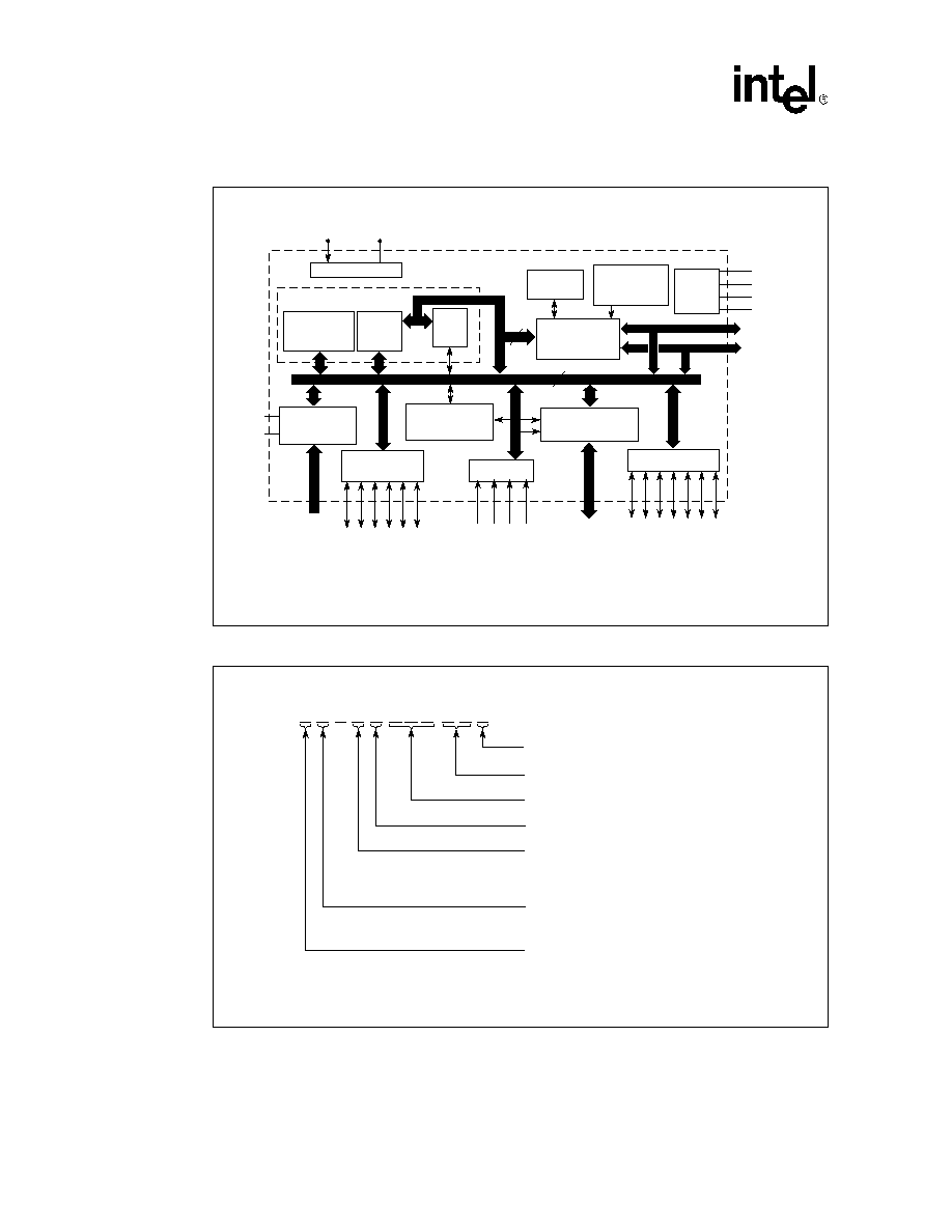
Figure 1. Block Diagram
Figure 2. 8XC196Kx, Jx, and CA Family Nomenclature
A4643-01
Clock Generator
PORT0
EPA0 - 9
ACH0 - 7
PORT1
T2CLK
T2DIR
T1CLK
T1DIR
PORT2
PORT3
PORT4
PORT5
SC0
SC1
SD0
SD1
TXD
RXD
PORT6
I/O Ports
Timer 1 & 2
Register
RAM
A/D Converter
(10-Bit)
[8 Channels]
Peripheral
Transaction
Server (PTS)
Power
and
GND
ALU
XTAL2
Control Signals
ADDR/
Data Bus
XTAL1
16
Code
RAM
On-chip
EPROM
(optional)
Event Processor
Array (EPA)
Programmable
Interrupt
Controller
Serial I/O
(UART & SSIO)
V
CC
V
SS
V
SS
V
SS
V
REF
ANGND
16
Memory
Controller with
Prefetch Queue
A4644-02
A N 8 7 C
R
K
1 9 6
0 = ROMless
3 = Masked ROM
7 = EPROM, OTP, QROM
Product Designation: KR, JV, JT, JR, CA
Frequency Designation (no mark = 16 MHz)
Product Family
CHMOS Technology
Program Memory Options:
N = PLCC (plastic leaded chip carrier)
Package Type Options:
A = -40
∞
C to +125
∞
C
ambient with
Intel Standard Burn-in
Temperature and Burn-in Options:

Automotive --
87C196KR, JV, JT, JR, CA Microcontrollers
Datasheet
9
3.0
Packaging Information
Figure 3. 87C196KR 68-Pin PLCC Package Diagram
A4645-02
P6.2 / T1CLK
P6.1 / EPA9
P6.0 / EPA8
P1.0 / EPA0 / T2CLK
P1.1 / EPA1
P1.2 / EPA2 / T2DIR
P1.3 / EPA3
P1.4 / EPA4
P1.5 / EPA5
P1.6 / EPA6
P1.7 / EPA7
V
REF
ANGND
P0.7 / ACH7
P0.6 / ACH6
P0.5 / ACH5
P0.4 / ACH4
WR# / WRL# / P5.2
BHE# / WRH# / P5.5
RD# / P5.3
V
PP
V
SS
ALE / ADV# / P5.0
INST / P5.1
READY / P5.6
P5.4 / SLPINT
V
SS
XTAL1
XTAL2
P6.7 / SD1
P6.6 / SC1
P6.5 / SD0
P6.4 / SC0
P6.3 / T1DIR
BUSWIDTH / P5.7
AD15 / P4.7
AD14 / P4.6
AD13 / P4.5
AD12 / P4.4
AD11 / P4.3
AD10 / P4.2
AD9 / P4.1
AD8 / P4.0
AD7 / P3.7
AD6 / P3.6
AD5 / P3.5
AD4 / P3.4
AD3 / P3.3
AD2 / P3.2
AD1 / P3.1
AD0 / P3.0
60
59
58
57
56
55
54
53
52
51
50
49
48
47
46
45
44
87C196KR
68-Pin
PLCC
View of component as
mounted on PC board
10
11
12
13
14
15
16
17
18
19
20
21
22
23
24
25
26
RESET#
NMI
EA#
V
SS
V
CC
P2.0 /
TXD
P2.1 / RXD
P2.2 / EXTINT
P2.3 / BREQ#
P2.4 / INT
OUT#
P2.5 / HLD#
P2.6 / HLD
A#
P2.7 / CLK
OUT
P0.0 / A
CH0
P0.1 / A
CH1
P0.2 / A
CH2
P0.3 / A
CH3
27
28
29
30
31
32
33
34
35
36
37
38
39
40
41
42
43
9
8
7
6
5
4
3
2
1
68
67
66
65
64
63
62
61
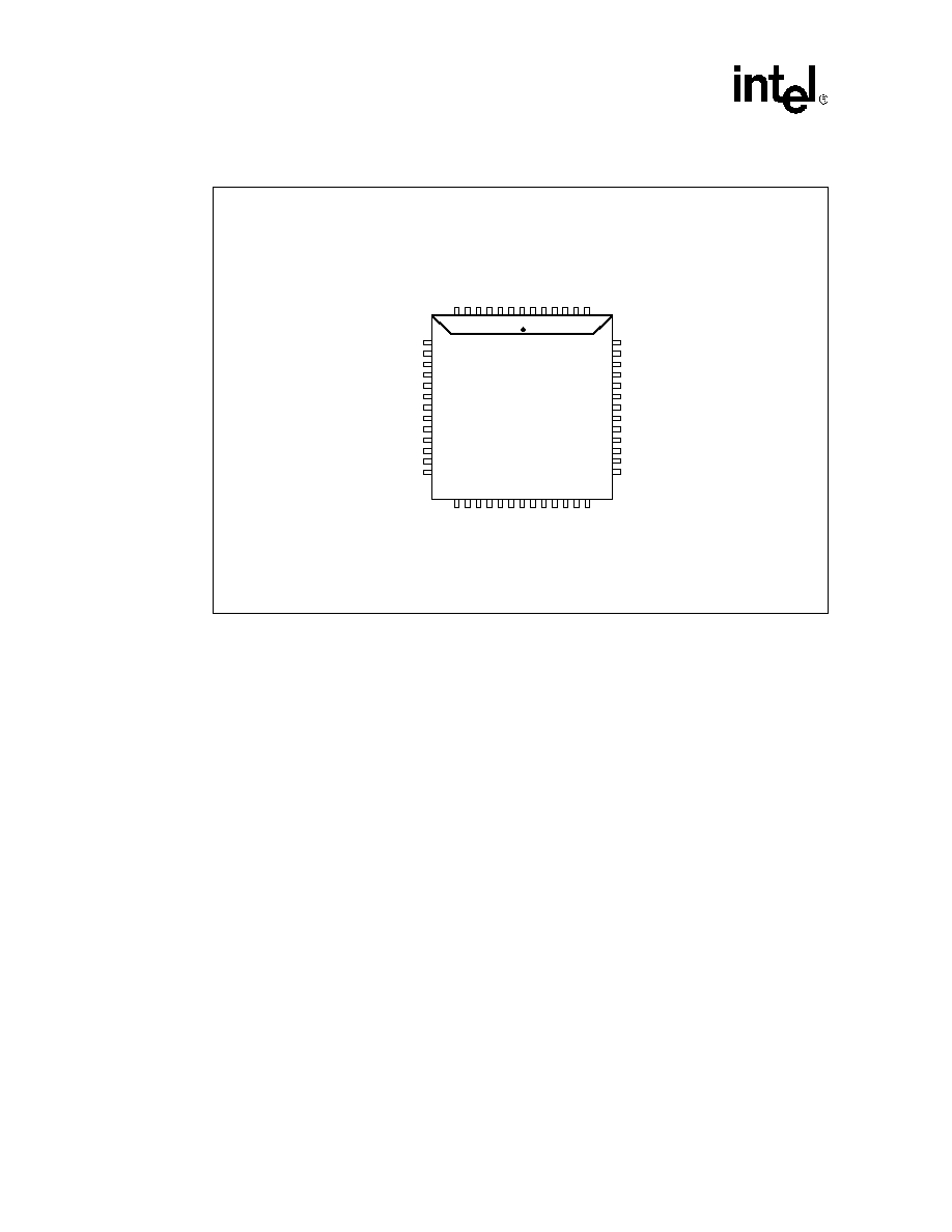
87C196KR, JV, JT, JR, CA Microcontrollers
-- Automotive
10
Datasheet
Figure 4. 87C196JV, JT, JR 52-Pin PLCC Package Diagram
A4646-02
P6.1 / EPA9
P6.0 / EPA8
P1.0 / EPA0
P1.1 / EPA1
P1.2 / EPA2
P1.3 / EPA3
V
REF
ANGND
P0.7 / ACH7
P0.6 / ACH6
P0.5 / ACH5
P0.4 / ACH4
P0.3 / ACH3
AD15 / P4.7
WR# / WRL# / P5.2
RD# / P5.3
V
PP
V
SS
ALE / ADV# / P5.0
V
SS
XTAL1
XTAL2
P6.7 / SD1
P6.6 / SC1
P6.5 / SD0
P6.4 / SC0
AD14 / P4.6
AD13 / P4.5
AD12 / P4.4
AD11 / P4.3
AD10 / P4.2
AD9 / P4.1
AD8 / P4.0
AD7 / P3.7
AD6 / P3.6
AD5 / P3.5
AD4 / P3.4
AD3 / P3.3
AD2 / P3.2
46
45
44
43
42
41
40
39
38
37
36
35
34
87C196JV
87C196JT
87C196JR
52-Pin
PLCC
View of component as
mounted on PC board
8
9
10
11
12
13
14
15
16
17
18
19
20
AD1 / P3.1
AD0 / P3.0
RESET#
EA#
V
SS
V
CC
P2.0 /
TXD
P2.1 / RXD
P2.2 / EXTINT
P2.4
P2.6
P2.7 / CLK
OUT
P0.2 / A
CH2
21
22
23
24
25
26
27
28
29
30
31
32
33
7
6
5
4
3
2
1
52
51
50
49
48
47
Automotive --
87C196KR, JV, JT, JR, CA Microcontrollers
Datasheet
11
Figure 5. 87C196CA 68-Pin PLCC Package Diagram
A4676-01
NC
NC
V
CC
EPA9 / P6.1
EPA8 / P6.0
EPA0 / P1.0 / T2CLK
EPA1 / P1.1
EPA2 / P1.2 / T2DIR
EPA3 / P1.3
NC
V
REF
ANGND
ACH7 / P0.7
ACH6 / P0.6
ACH5 / P0.5
ACH4 / P0.4
NC
WR# / P5.2
WRH# / P5.5
RD# / P5.3
V
PP
V
SS
ALE / P5.0
READY / P5.6
P5.4
V
SS1
XTAL1
XTAL2
RXCAN
TXCAN
SD1 / P6.7
SC1 / P6.6
SD0 / P6.5
SC0 / P6.4
NC
AD15 / P4.7
AD14 / P4.6
AD13 / P4.5
AD12 / P4.4
AD11 / P4.3
AD10 / P4.2
AD9 / P4.1
AD8 / P4.0
AD7 / P3.7
AD6 / P3.6
AD5 / P3.5
AD4 / P3.4
AD3 / P3.3
AD2 / P3.2
NC
NC
60
59
58
57
56
55
54
53
52
51
50
49
48
47
46
45
44
87C196CA
68 ≠ ld PLCC
View of component as
mounted on PC board
10
11
12
13
14
15
16
17
18
19
20
21
22
23
24
25
26
P3.1 / AD1
P3.0 / AD0
RESET#
NMI
EA#
V
SS1
V
CC
V
SS
TXD / P2.0
RXD / P2.1
EXTINT / P2.2
P2.4
P2.6
CLKOUT / P2.7
ACH2 / P0.2
ACH3 / P0.3
NC
27
28
29
30
31
32
33
34
35
36
37
38
39
40
41
42
43
9
8
7
6
5
4
3
2
1
68
67
66
65
64
63
62
61
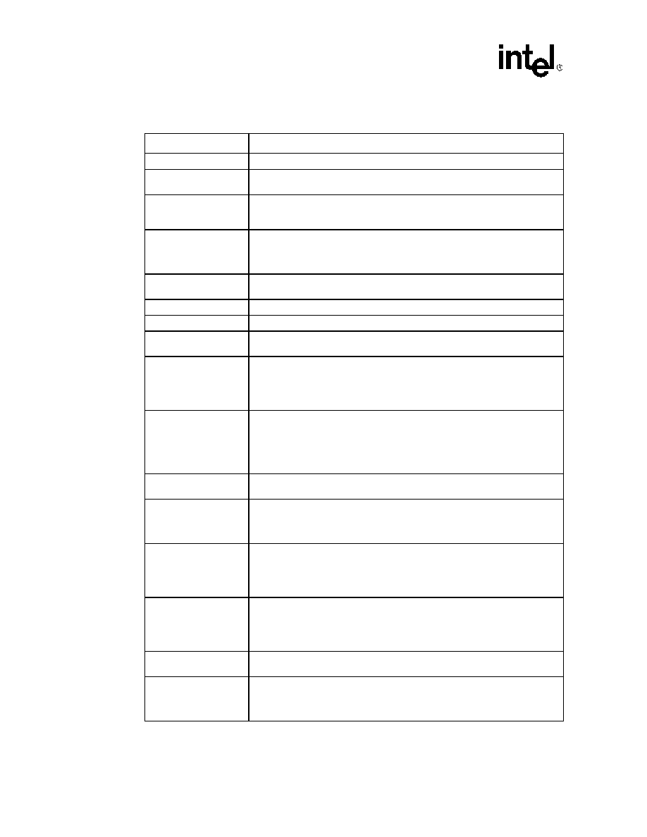
87C196KR, JV, JT, JR, CA Microcontrollers
-- Automotive
12
Datasheet
Table 2. Pin Descriptions (Sheet 1 of 2)
Symbol
Name and Function
V
CC
Main supply voltage (+5 V).
V
SS
Digital circuit ground (0 V). There are three V
SS
pins, all of which MUST be
connected to a single ground plane.
V
REF
Reference for the A/D converter (+5 V). V
REF
is also the supply voltage to the
analog portion of the A/D converter and the logic used to read Port 0. Must be
connected for A/D and Port 0 to function.
V
PP
Programming voltage for the EPROM parts. It should be +12.5 V for programming.
It is also the timing pin for the return from powerdown circuit. Connect this pin with
a 1 µF capacitor to V
SS
and a 1 M
resistor to V
CC
. If this function is not used, V
PP
may be tied to V
CC
.
ANGND
Reference ground for the A/D converter. Must be held at nominally the same
potential as V
SS
.
XTAL1
Input of the oscillator inverter and the internal clock generator.
XTAL2
Output of the oscillator inverter.
P2.7/CLKOUT
Output of the internal clock generator. The frequency is Ω the oscillator frequency.
It has a 50% duty cycle. Also LSIO pin when not used as CLKOUT.
RESET#
Reset input to the chip. Input low for at least 16 state times will reset the chip. The
subsequent low to high transition resynchronizes CLKOUT and commences a 10-
state time sequence in which the PSW is cleared, bytes are read from 2018H and
201AH loading the CCBs, and a jump to location 2080H is executed. Input high for
normal operation. RESET# has an internal pullup.
P5.7/BUSWIDTH
Input for bus width selection. If CCR bit 1 is a one and CCR1 bit 2 is a one, this pin
dynamically controls the Bus width of the bus cycle in progress. If BUSWIDTH is
low, an 8-bit cycle occurs. If BUSWIDTH is high, a 16-bit cycle occurs. If CCR bit 1
is "0" and CCR1 bit 2 is "1", all bus cycles are 8-bit; if CCR bit 1 is "1" and CCR1 bit
2 is "0", all bus cycles are 16-bit. CCR bit 1 ="0'' and CCR1 bit 2 = "0" is illegal.
Also an LSIO pin when not used as BUSWIDTH.
NMI
A positive transition causes a non-maskable interrupt vector through memory
location 203EH.
P5.1/INST
Output high during an external memory read indicates the read is an instruction
fetch. INST is valid throughout the bus cycle. INST is active only during external
memory fetches. During internal [EP]ROM fetches INST is held low. Also LSIO
when not INST.
EA#
Input for memory select (External Access). EA# equal to a high causes memory
accesses within the [EP]ROM address space to be directed to on-chip EPROM/
ROM. EA# equal to a low causes accesses to these locations to be directed to off-
chip memory. EA# = +12.5 V causes execution to begin in the Programming
Mode. EA# latched at reset.
P5.0/ALE/ADV#
Address Latch Enable or Address Valid output, as selected by CCR. Both pin
options provide a latch to demultiplex the address from the address/data bus.
When the pin is ADV#, it goes inactive (high) at the end of the bus cycle. ADV#
can be used as a chip select for external memory. ALE/ADV# is active only during
external memory accesses. Also LSIO when not used as ALE.
P5.3/RD#
Read signal output to external memory. RD# is active only during external memory
reads. LSIO when not used as RD#.
P5.2/WR#/WRL#
Write and Write Low output to external memory, as selected by the CCR, WR# will
go low for every external write, while WRL# will go low only for external writes
where an even byte is being written. WR#/WRL# is active during external memory
writes. Also an LSIO pin when not used as WR#/WRL#.

Automotive --
87C196KR, JV, JT, JR, CA Microcontrollers
Datasheet
13
P5.5/BHE#/WRH#
Byte High Enable or Write High output, as selected by the CCR. BHE# = 0 selects
the bank of memory that is connected to the high byte of the data bus. A0 = 0
selects that bank of memory that is connected to the low byte. Thus accesses to a
16-bit wide memory can be to the low byte only (A0 = 0, BHE# =1), to the high byte
only (A0 = 1, BHE# = 0) or both bytes (A0 = 0, BHE# = 0). If the WRH# function is
selected, the pin will go low if the bus cycle is writing to an odd memory location.
BHE#/WRH# is only valid during 16-bit external memory write cycles. Also an
LSIO pin when not BHE#/WRH#.
P5.6/READY
Ready input to lengthen external memory cycles, for interfacing with slow or
dynamic memory, or for bus sharing. If the pin is high, CPU operation continues in
a normal manner. If the pin is low prior to the falling edge of CLKOUT, the memory
controller goes into a wait state mode until the next positive transition in CLKOUT
occurs with READY high. When external memory is not used, READY has no
effect. The max number of wait states inserted into the bus cycle is controlled by
the CCR/CCR1. Also an LSIO pin when READY is not selected.
P5.4/SLPINT
Dual functional I/O pin. As a bidirectional port pin (LSIO) or as a system function.
The system function is a Slave Port Interrupt Output Pin.
P6.2/T1CLK
Dual function I/O pin. Primary function is that of a bidirectional I/O pin (LSIO);
however it may also be used as a TIMER1 Clock input. The TIMER1 will increment
or decrement on both positive and negative edges of this pin.
P6.3/T1DIR
Dual function I/O pin. Primary function is that of a bidirectional I/O pin (LSIO);
however it may also be used as a TIMER1 Direction input. The TIMER1 will
increment when this pin is high and decrements when this pin is low.
PORT1/EPA0≠7
P6.0≠6.1/EPA8≠9
Dual function I/O port pins. Primary function is that of bidirectional I/O (LSIO).
System function is that of High Speed capture and compare. EPA0 and EPA2
have yet another function of T2CLK and T2DIR of the TIMER2 timer/counter.
PORT 0/ACH0≠7
8-bit high impedance input-only port. These pins can be used as digital inputs and/
or as analog inputs to the on-chip A/D converter. These pins are also used as
inputs to EPROM parts to select the Programming Mode.
P6.4≠6.7/SSIO
Dual function I/O ports that have a system function as Synchronous Serial I/O.
Two pins are clocks and two pins are data, providing full duplex capability.
PORT 2
8-bit multi-functional port. All of its pins are shared with other functions.
PORT 3 and 4
8-bit bidirectional I/O ports with open drain outputs. These pins are shared with the
multiplexed address/data bus which has strong internal pullups.
TXCAN
Push-pull output to the CAN bus line.
RXCAN
High-impedance input-only from the CAN bus line.
Table 2. Pin Descriptions (Sheet 2 of 2)
Symbol
Name and Function

87C196KR, JV, JT, JR, CA Microcontrollers
-- Automotive
14
Datasheet
4.0
Electrical Characteristics
Note:
This document contains information on products in production. The specifications are subject to
change without notice.
4.1
Absolute Maximum Ratings
Warning:
Stressing the device beyond the "Absolute Maximum Ratings" may cause permanent damage.
These are stress ratings only.
4.2
Operating Conditions
Warning:
Operation beyond the "Operating Conditions" is not recommended and extended exposure beyond
the "Operating Conditions" may affect device reliability.
Table 3. Absolute Maximum Ratings
Parameter
Maximum Rating
Storage Temperature
≠60∞C to +150∞C
Voltage from V
PP
or EA# to V
SS
or ANGND
≠0.5 V to +13.0 V
Voltage from any other pin to V
SS
or ANGND
≠0.5 V to +7.0 V
Power Dissipation
0.5 W
Table 4. Operating Conditions
Parameter
Values
T
A
(Ambient Temperature Under Bias)
≠40∞C to +125∞C
V
CC
(Digital Supply Voltage)
4.50 V to 5.50 V
V
REF
(Analog Supply Voltage) (Notes 1, 2)
4.50 V to 5.50 V
F
OSC
(Oscillator Frequency):
4 MHz to 16 MHz
(2)
NOTE:
1. ANGND and V
SS
should be nominally at the same potential.
2. Device is static and should operate below 1 Hz, but only tested down to 4 MHz.

Automotive --
87C196KR, JV, JT, JR, CA Microcontrollers
Datasheet
15
4.3
DC Characteristics
Table 5. DC Characteristics (Sheet 1 of 2)
Symbol
Parameter
Min
Typical
Max
Units
Test Conditions
I
CC
V
CC
supply current
(≠40∞C to +125∞C
ambient)
50
75
(JV=80)
(CA=90)
mA
X
TAL1
= 16 MHz,
V
CC
= V
PP
= V
REF
= 5.5 V
(While device is in reset)
I
CC1
Active mode supply
current (typical)
50
(JV=55)
mA
I
REF
A/D reference supply
current
2
5
mA
I
IDLE
Idle mode current
15
30
(JV=32)
(CA=40)
mA
X
TAL
1
= 16 MHz,
V
CC
= V
PP
= V
REF
= 5.5 V
I
PD
Powerdown mode
current
50
µA
V
CC
= V
PP
= V
REF
= 5.5 V
(Note 4)
V
IL
Input low voltage
(all pins)
≠0.5 V
0.3 V
CC
V
V
IH
Input high voltage (all
pins)
0.7 V
CC
V
CC
+ 0.5
V
(Note 5)
V
OL
Output low voltage
(outputs configured as
push/pull)
0.3
0.45
1.5
V
I
OL
= 200 µA (Note 3)
I
OL
= 3.2 mA
I
OL
= 7.0 mA
V
OH
Output high voltage
(outputs configured as
complementary)
V
CC
≠ 0.3
V
CC
≠ 0.7
V
CC
≠ 1.5
V
I
OH
= ≠ 200 µA (Note 3)
I
OH
= ≠ 3.2 mA
I
OH
= ≠ 7.0 mA
I
LI
Input leakage current
(standard inputs)
± 8
JT,JV,CA:
±10
µA
V
SS
V
IN
V
CC
(Note 2)
I
LI1
Input leakage current
(Port 0--A/D inputs)
± 1
JT,JV: ±2
CA: ±1.5
µA
V
SS
V
IN
V
CC
I
IH
Input high current (NMI
pin)
+175
µA
V
SS
V
IN
V
CC
V
OH1
SLPINT (P5.4) and
HLDA (P2.6) Output
high voltage in RESET
2.0
V
I
OH
= 0.8 mA (Note 8)
V
OH2
Output high voltage in
RESET
V
CC
≠ 1 V
V
I
OH
= ≠ 15 µA (Notes 1, 6)
NOTES:
1. All BD (bidirectional) pins except P5.5/INST and P2.7/CLKOUT which are excluded due to their not being
weakly pulled high in reset. BD pins include Port1, Port 2, Port3, Port4, Port5, and Port6.
2. Standard Input pins include XTAL1, EA#, RESET#, and Ports 1,2,3,4,5,6 when configured as inputs.
3. All bidirectional I/O pins when configured as outputs (push/pull).
4. Typicals are based on limited number of samples and are not guaranteed. The values listed are at room
temperature and V
REF
= V
CC
= 5.0 V.
5. V
IH
max for Port0 is V
REF
+ 0.5 V.
6. Refer to "VOH2/IOH2 Specification" errata #1 in errata section of this datasheet.
7. This specification is not tested in production and is based upon theoretical estimates and/or product
characterization.
8. Violating these specifications in reset may cause the device to enter test modes (P5.4 and P2.6).

87C196KR, JV, JT, JR, CA Microcontrollers
-- Automotive
16
Datasheet
I
OH2
(KR)
Output high current in
RESET
≠6
≠15
≠20
≠35
≠60
≠70
µA
V
OH2
= V
CC
≠ 1.0 V
V
OH2
= V
CC
≠ 2.5 V
V
OH2
= V
CC
≠ 4.0 V
I
OH2
(JV, JT,
JR,CA)
Output High Current in
RESET
≠30
≠75
≠90
≠120
≠240
≠280
µA
V
OH2
= V
CC
≠ 1.0 V
V
OH2
= V
CC
≠ 2.5 V
V
OH2
= V
CC
≠ 4.0 V
R
RST
Reset pullup resistor
6 K
65 K
V
OL3
Output low voltage in
reset (RESET pin only)
0.3
0.5
0.8
V
I
OL3
= 4 mA (Note 7)
I
OL3
= 6 mA
I
OL3
= 10 mA
C
S
Pin Capacitance (any
pin to V
SS
)
10
pF
F
TEST
= 1.0 MHz
R
WPU
Weak pullup resistance
(approx.)
150 K
(Note 4)
Figure 6. 87C196KR and JR I
CC
vs. Frequency
Table 5. DC Characteristics (Sheet 2 of 2)
Symbol
Parameter
Min
Typical
Max
Units
Test Conditions
NOTES:
1. All BD (bidirectional) pins except P5.5/INST and P2.7/CLKOUT which are excluded due to their not being
weakly pulled high in reset. BD pins include Port1, Port 2, Port3, Port4, Port5, and Port6.
2. Standard Input pins include XTAL1, EA#, RESET#, and Ports 1,2,3,4,5,6 when configured as inputs.
3. All bidirectional I/O pins when configured as outputs (push/pull).
4. Typicals are based on limited number of samples and are not guaranteed. The values listed are at room
temperature and V
REF
= V
CC
= 5.0 V.
5. V
IH
max for Port0 is V
REF
+ 0.5 V.
6. Refer to "VOH2/IOH2 Specification" errata #1 in errata section of this datasheet.
7. This specification is not tested in production and is based upon theoretical estimates and/or product
characterization.
8. Violating these specifications in reset may cause the device to enter test modes (P5.4 and P2.6).
A4647-02
I
CC
Max
I
CC
Typical
I
IDLE
Max
I
IDLE
Typical
80
70
60
50
40
30
20
10
0
4 MHz
10 MHz
15 MHz
I
CC
= [mA]
KR/JR I
CC
vs. Frequency
Notes:
I
IDLE
Max = 1.65 x Freq + 2.2
I
CC
Max = 3.88 x Freq + 13.43

Automotive --
87C196KR, JV, JT, JR, CA Microcontrollers
Datasheet
17
Figure 7. JT I
CC
vs. Frequency
Figure 8. 87C196CA I
CC
vs. Frequency
A5877-01
0
0
4 MHz
10 MHz
20 MHz
20
30
40
10
50
60
70
Note:
90
I
CC
vs Frequency
I
CC
Max
I
CC
(mA)
I
IDLE
Max
I
IDLE
Max = 1.25 x FREQ + 15
I
CC
Max = 3.25 x FREQ + 23
A5862-01
90
80
70
60
50
40
30
20
10
0
2
8
14
20
Active I
CC
Max = 90 mA
Active I
CC
= 75 mA
Idle Max
= 40 mA
Idle I
CC
= 32 mA
I
CC
(mA)
87C196KR, JV, JT, JR, CA Microcontrollers
-- Automotive
18
Datasheet
4.4
AC Characteristics
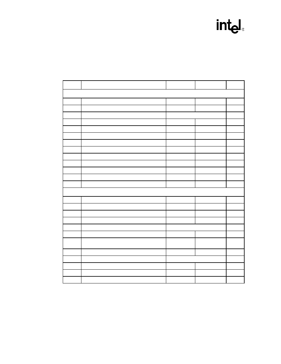
Table 6. AC Characteristics (Sheet 1 of 2)
(over specified operating conditions); Test conditions: capacitance load on all
pins = 100 pF, Rise and fall times = 10 ns, F
OSC
= 16 MHz
Symbol
Parameter
Min
Max
Units
The system must meet these specifications to work with the 87C196KR, JV, JT, JR, CA Microcontroller.
T
AVYV
Address Valid to READY Setup
2 T
OSC
≠ 75
ns
T
LLYV
ALE Low to READY Setup
T
OSC
≠ 70
ns
T
YLYH
Non Ready Time
No Upper Limit
ns
T
CLYX
READY Hold after CLKOUT Low
0
T
OSC
≠ 30
ns
(1)
T
LLYX
READY Hold after ALE Low
T
OSC
≠ 15
2 T
OSC
≠ 40
ns
(1)
T
AVGV
Address Valid to Buswidth Setup
2 T
OSC
≠ 75
ns
T
LLGV
ALE Low to Buswidth Setup
T
OSC
≠ 60
ns
T
CLGX
Buswidth Hold after CLKOUT Low
0
ns
T
AVDV
Address Valid to Input Data Valid
3 T
OSC
≠ 55
ns
T
RLDV
RD# Active to Input Data Valid
T
OSC
≠ 22
ns
T
CLDV
CLKOUT Low to Input Data Valid
T
OSC
≠ 50
ns
T
RHDZ
End of RD# to Input Data Float
T
OSC
ns
T
RXDX
Data Hold after RD# Inactive
0
ns
The 87C196KR, JV, JT, JR, CA Microcontroller meets these specifications.
F
XTAL
Oscillator Frequency
4
16
MHz
(2)
T
OSC
Oscillator Period (1/F
XTAL
)
62.5
250
ns
T
XHCH
XTAL1 High to CLKOUT High or Low
20
110
ns
(3)
T
OFD
Clock Failure to Reset Pulled Low
4
40
µS
(7)
T
CLCL
CLKOUT Period
2 T
OSC
ns
T
CHCL
CLKOUT High Period
T
OSC
≠ 10
T
OSC
+ 15
ns
T
CLLH
CLKOUT Falling Edge to ALE Rising
≠10
CA: ≠15
15
CA: 10
ns
T
LLCH
ALE/ADV# Falling Edge to CLKOUT Rising
≠20
15
ns
T
LHLH
ALE/ADV# Cycle Time
4 T
OSC
ns
T
LHLL
ALE/ADV# High Period
T
OSC
≠ 10
T
OSC
+ 10
ns
T
AVLL
Address Setup to ALE/ADV# Falling Edge
T
OSC
≠ 15
ns
T
LLAX
Address Hold after ALE/ADV# Falling Edge
T
OSC
≠ 40
ns
NOTES:
1. If max is exceeded, additional wait states will occur.
2. Testing performed at 4 MHz; however, the device is static by design and will typically operate below 1 Hz.
3. Typical specifications, not guaranteed.
4. Assuming back-to-back bus cycles.
5. 8-bit bus only.
6. T
RLAZ
(max) = 5 ns by design.
7. T
OFD
is the time for the oscillator fail detect circuit (OFD) to react to a clock failure.
Automotive --
87C196KR, JV, JT, JR, CA Microcontrollers
Datasheet
19
T
LLRL
ALE/ADV# Falling Edge to RD# Falling Edge
T
OSC
≠ 30
ns
T
RLCL
RD# Low to CLKOUT Falling Edge
4
30
ns
T
RLRH
RD# Low Period
T
OSC
≠ 5
CA: T
OSC
≠ 10
ns
T
RHLH
RD# Rising Edge to ALE/ADV# Rising Edge
T
OSC
T
OSC
+ 25
ns
(4)
T
RLAZ
RD# Low to Address Float
5
ns
(6)
T
LLWL
ALE/ADV# Falling Edge to WR# Falling Edge
T
OSC
≠ 10
ns
T
CLWL
CLKOUT Low to WR# Falling Edge
≠5
25
ns
T
QVWH
Data Stable to WR# Rising Edge
T
OSC
≠ 23
ns
T
CHWH
CLKOUT High to WR# Rising Edge
≠10
15
ns
T
WLWH
WR# Low Period
T
OSC
≠ 20
ns
T
WHQX
Data Hold after WR# Rising Edge
T
OSC
≠ 25
ns
T
WHLH
WR# Rising Edge to ALE/ADV# Rising Edge
T
OSC
≠ 10
T
OSC
+ 15
ns
(4)
T
WHBX
BHE#, INST Hold after WR# Rising Edge
T
OSC
≠ 10
ns
T
WHAX
AD[15:8] Hold after WR# Rising Edge
T
OSC
≠ 30
ns
(5)
T
RHBX
BHE#, INST Hold after RD# Rising Edge
T
OSC
≠ 10
ns
T
RHAX
AD[15:8] Hold after RD# Rising Edge
T
OSC
≠ 30
ns
(5)
Table 6. AC Characteristics (Sheet 2 of 2)
(over specified operating conditions); Test conditions: capacitance load on all
pins = 100 pF, Rise and fall times = 10 ns, F
OSC
= 16 MHz
Symbol
Parameter
Min
Max
Units
NOTES:
1. If max is exceeded, additional wait states will occur.
2. Testing performed at 4 MHz; however, the device is static by design and will typically operate below 1 Hz.
3. Typical specifications, not guaranteed.
4. Assuming back-to-back bus cycles.
5. 8-bit bus only.
6. T
RLAZ
(max) = 5 ns by design.
7. T
OFD
is the time for the oscillator fail detect circuit (OFD) to react to a clock failure.
87C196KR, JV, JT, JR, CA Microcontrollers
-- Automotive
20
Datasheet
Figure 9. System Bus Timing
A4649-01
XTAL1
CLKOUT
ALE
RD#
WR#
BHE#,
INST
T
OSC
T
XHCH
T
CHCL
T
CLCL
T
CLCH
T
LLCH
T
LHLH
T
LHLL
T
LLRL
T
RLRH
T
RHLH
T
RHDZ
T
AVLL
T
LLAX
T
RLDV
Address Out
Data In
T
AVDV
T
LLWL
T
WLWH
T
WHLH
T
QVWH
T
WHQX
Data Out
Address Out
Address Out
Valid
Address Out
T
WHAX
, T
RHAX
T
WHBX
, T
RHBX
T
RLAZ
BUS
BUS
AD15:8
Automotive --
87C196KR, JV, JT, JR, CA Microcontrollers
Datasheet
21
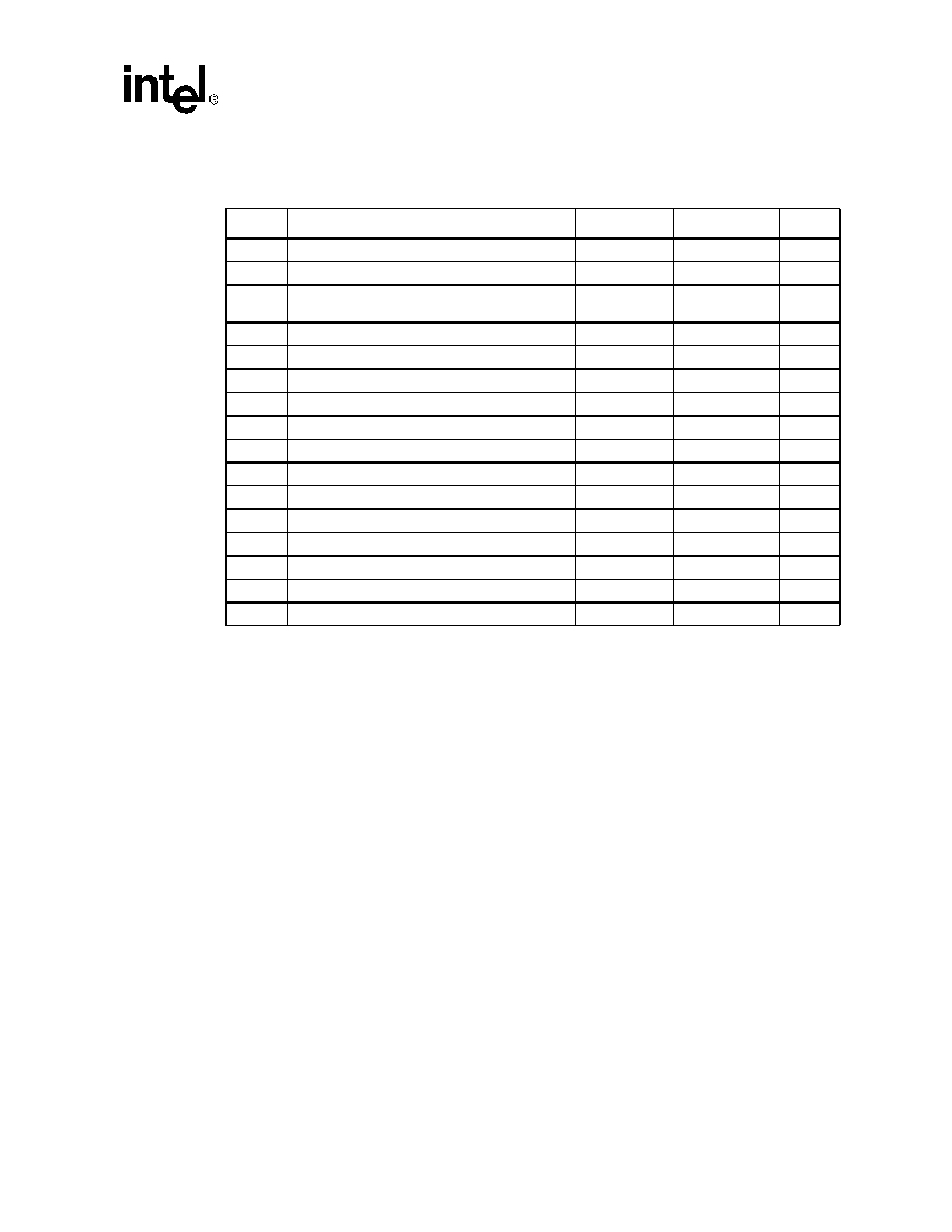
Figure 10. READY/Buswidth Timing
Table 7. External Clock Drive
Symbol
Parameter
Min
Max
Units
1/T
XLXL
Oscillator Frequency
4
16
MHz
T
XLXL
Oscillator Period (T
OSC
)
62.5
250
ns
T
XHXX
High Time
0.35 T
OSC
0.65 T
OSC
ns
T
XLXX
Low Time
0.35 T
OSC
0.65 T
OSC
ns
T
XLXH
Rise Time
10
ns
T
XHXL
Fall Time
10
ns
Figure 11. External Clock Drive Waveforms
A4650-01
XTAL1
CLKOUT
ALE
RD#
READY
T
OSC
T
XHCH
T
CHCL
T
CLCL
T
CLLH
T
LLYX
T
AVYV
T
AVGV
T
LLYV
T
LLGV
T
CLYX
T
CLGX
BUSWIDTH
BUS
Address Out
Data
A5842-01
T
XLXX
T
XHXX
T
XHXL
T
XLXL
0.3 V
CC
≠ 0.5 V
0.7 V
CC
+ 0.5 V
T
XLXH
0.7 V
CC
+ 0.5 V
0.3 V
CC
≠ 0.5 V
0.7 V
CC
+ 0.5 V
87C196KR, JV, JT, JR, CA Microcontrollers
-- Automotive
22
Datasheet
Figure 12. AC Testing Input, Output Waveforms
Figure 13. Float Waveforms
Table 8. Thermal Characteristics
Device and Package
JA
JC
AN87C196KR
(68-Lead PLCC)
41∞C/W
14∞C/W
AN87C196JV, JT, JR
(52-Lead PLCC)
42∞C/W
15∞C/W
AN87C196CA
(68-Lead PLCC)
36.5∞C/W
10∞C/W
NOTES:
1.
JA
= Thermal resistance between junction and the surrounding environment (ambient). Measurements are
taken 1 ft. away from case in air flow environment.
JC
= Thermal resistance between junction and package surface (case).
2. All values of
JA
and
JC
may fluctuate depending on the environment (with or without airflow, and how
much airflow) and device power dissipation at temperature of operation. Typical variations are ±2 ∞C/W.
3. Values listed are at a maximum power dissipation of 0.50 W.
A4651-01
Test Points
INPUTS
OUTPUTS
2.0 V
0.8 V
Note:
AC testing inputs are driven at 3.5 V for a logic " 1" and 0.45 V for a logic
" 0" . Timing measurements are made at 2.0 V for a logic " 1" and 0.8 V for
a logic " 0".
3.5 V
0.45 V
A5844-01
V
LOAD
V
LOAD
≠ 0.15 V
V
LOAD
+ 0.15 V
Timing Reference
Points
V
OH
≠ 0.15 V
V
OL
+ 0.15 V
Note:
For timing purposes, a port pin is no longer floating when a 150 mV change from load
voltage occurs and begins to float when a 150 mV change from the loading V
OH
/V
OL
level occurs with I
OL
/I
OH
15 mA.
Automotive --
87C196KR, JV, JT, JR, CA Microcontrollers
Datasheet
23
4.4.1
Explanation of AC Symbols
Each symbol is two pairs of letters prefixed by "t" for time. The characters in a pair indicate a
signal and its condition, respectively. Symbols represent the time between the two signal/condition
points.
4.4.2
EPROM Specifications
Conditions
Signals
H≠High
A≠Address
HA≠HLDA#
L≠Low
B≠BHE#
L≠ALE/ADV#
V≠Valid
C≠CLKOUT
R≠RD#
X≠No Longer Valid
D≠DATA
W≠WR#/WRH#/WRI#
Z≠Floating
G≠Buswidth
X≠XTAL1
H≠HOLD#
Y≠READY
Table 9. AC EPROM Programming Characteristics
Operating Conditions: Load Capacitance = 150 pF; T
C
= 25∞C ± 5∞C; V
REF
= 5.0 V ± 0.5 V; V
SS,
ANGND = 0 V;
V
PP
= 12.5 V ± 0.25 V; EA# = 12.5 V ± 0.25 V; F
OSC
= 5.0 MHz
Symbol
Parameter
Min
Max
Units
T
AVLL
Address Setup Time
0
T
OSC
T
LLAX
Address Hold Time
100
T
OSC
T
DVPL
Data Setup Time
0
T
OSC
T
PLDX
Data Hold Time
400
T
OSC
T
LLLH
PALE# Pulse Width
50
T
OSC
T
PLPH
PROG# Pulse Width
(3)
50
T
OSC
T
LHPL
PALE# High to PROG# Low
220
T
OSC
T
PHLL
PROG# High to Next PALE# Low
220
T
OSC
T
PHDX
Word Dump Hold Time
50
T
OSC
T
PHPL
PROG# High to Next PROG# Low
220
T
OSC
T
PLDV
PROG# Low to Word Dump Valid
50
T
OSC
T
SHLL
RESET# High to First PALE# Low
1100
T
OSC
T
PHIL
PROG# High to AINC# Low
0
T
OSC
T
ILIH
AINC# Pulse Width
240
T
OSC
T
ILVH
PVER Hold after AINC# Low
50
T
OSC
T
ILPL
AINC# Low to PROG# Low
170
T
OSC
T
PHVL
PROG# High to PVER# Valid
220
T
OSC
NOTES:
1. Run-time programming is done with F
OSC
= 6.0 MHz to 10.0 MHz, V
CC
, V
PD
, V
REF
= 5 V ± 0.5 V,
TC = 25∞C ± 5 ∞C and V
PP
= 12.5 V ± 0.25 V. For run-time programming over a full operating range,
contact factory.
2. Programming specifications are not tested, but guaranteed by design.
3. This specification is for the word dump mode. For programming pulses, use 300 T
OSC
+ 100 µS.
87C196KR, JV, JT, JR, CA Microcontrollers
-- Automotive
24
Datasheet
Table 10. DC EPROM Programming Characteristics
Symbol
Parameter
Min
Max
Units
I
PP
V
PP
Programming Supply Current
100
CA: 200
mA
NOTE: V
PP
must be within 1 V of V
CC
while V
CC
< 4.5 V. V
PP
must not have a low impedance path to ground
or V
SS
while V
CC
> 4.5 V.
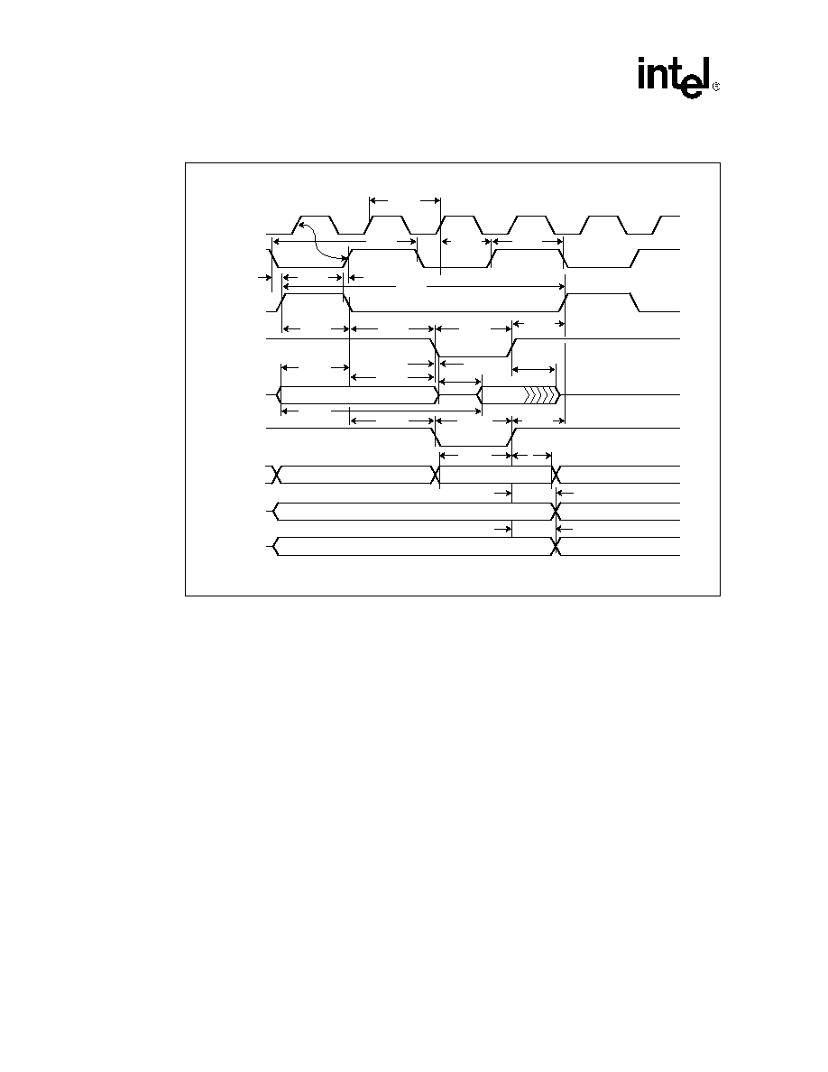
Figure 14. Slave Programming Mode Data Program Mode with Single Program Pulse
Figure 15. Slave Programming Mode in Word Dump or Data Verify Mode with Auto Increment
A5838-01
Address/Command
T
SHLL
T
PHVL
T
LLVH
Address/Command
Data
Valid
RESET#
PORTS 3/4
PALE#
P2.1
PROG#
P2.2
AINC#
P2.0
T
LLAX
T
LLLH
T
LHPL
T
PHDX
T
AVLL
T
DVPL
T
PLPH
T
PHLL
A5839-01
PORTS 3/4
RESET#
Address/Command
Ver Bits/WD Dump
T
SHLL
PROG#
P2.2
PALE#
P2.1
T
PLDV
PVER#
P2.0
T
ILPL
ADDR
ADDR + 2
T
PHDX
T
PLDV
T
PHDX
Ver Bits/WD Dump
T
PHPL
Automotive --
87C196KR, JV, JT, JR, CA Microcontrollers
Datasheet
25
4.4.3
A to D Converter Specifications
The speed of the A/D converter in the 10-bit or 8-bit modes can be adjusted by setting the
AD_TIME special function register to the appropriate value. The AD_TIME register only
programs the speed at which the conversions are performed, not the speed at which it can convert
correctly.
The converter is ratiometric, so absolute accuracy is dependent on the accuracy and stability of
V
REF
.
V
REF
must not exceed V
CC
by more than 0.5 V since it supplies both the resistor ladder and the
digital portion of the converter and input port pins.
For testing purposes, after a conversion is started, the device is placed in the IDLE mode until the
conversion is complete. Testing is performed at V
REF
= 5.12 V and 16 MHz operating frequency.
There is an AD_TEST register that allows for conversion on ANGND and V
REF
as well as zero
offset adjustment. The absolute error listed is without doing any adjustments.
Figure 16. Slave Programming Mode Timing in Data Program Mode with Repeated PROG
Pulse and Auto Increment
A5840-01
Data
P1
P2
T
PHPL
T
PHIL
T
ILPL
T
ILVH
T
ILIH
Address/Command
Data
RESET#
PORTS 3/4
PALE#
P2.1
PROG#
P2.2
PVER#
P2.0
AINC#
P2.4
Valid
For P2
Valid For P1
Table 11. A/D Operating Conditions (Sheet 1 of 2)
Symbol
Description
Min
Max
Units
T
A
Automotive Ambient Temperature
≠40
+125
∞C
V
CC
Digital Supply Voltage
4.50
5.50
V
V
REF
Analog Supply Voltage
4.50
5.50
V
NOTES:
1. ANGND and V
SS
should nominally be at the same potential.
2. V
REF
must not exceed V
CC
by more than +0.5 V.
3. Testing is performed at V
REF
= 5.12 V.
4. The value of AD_TIME must be selected to meet these specifications.

87C196KR, JV, JT, JR, CA Microcontrollers
-- Automotive
26
Datasheet
T
SAM
Sample Time
2.0
µS
T
CONV
Conversion Time
16.5
CA: 15
19.5
CA: 18
µS
F
OSC
Oscillator Frequency
4
16
MHz
Table 12. A/D Operating Parameter Values
Parameter
Typical
(,1)
Min
Max
Units
Resolution
1024
10
1024
10
Level
Bits
Absolute Error
0
≠3
+3
LSBs
Full Scale Error
±2
LSBs
Zero Offset Error
±2
LSBs
Non-linearity
±3
LSBs
Differential Non-linearity
> ≠0.5
+0.5
LSBs
Channel-to-Channel Matching
0
±1
LSBs
Repeatability
±0.25
0
LSBs
(
1
)
Temperature Coefficients:
Offset
Fullscale
Differential Non-linearity
0.009
0.009
0.009
LSB/C
(
1
)
Off Isolation
≠60
dB
(
1
)(
2
)(
3
)
Feedthrough
≠60
dB
(
1
)(
2
)
V
CC
Power Supply Rejection
≠60
dB
(
1
)(
2
)
Input Resistance
750
1.2 K
(1)
DC Input Leakage
0
±1
JT, JV = ±2
CA = ±3
µA
NOTES:
These values are expected for most parts at 25 ∞C but are not tested or guaranteed.
An "LSB," as used here, has a value of approximately 5 mV. (See Automotive Handbook for A/D glossary
of terms.)
1. These values are not tested in production and are based on theoretical estimates and/or laboratory test.
2. DC to 100 KHz.
3. Multiplexer break-before-make guaranteed.
Table 11. A/D Operating Conditions (Sheet 2 of 2)
Symbol
Description
Min
Max
Units
NOTES:
1. ANGND and V
SS
should nominally be at the same potential.
2. V
REF
must not exceed V
CC
by more than +0.5 V.
3. Testing is performed at V
REF
= 5.12 V.
4. The value of AD_TIME must be selected to meet these specifications.

Automotive --
87C196KR, JV, JT, JR, CA Microcontrollers
Datasheet
27
Table 13. HOLD#/HLDA# Timings
Symbol
Description
Min
Max
Units
Notes
T
HVCH
HOLD Setup
65
ns
Note 1
T
CLHAL
CLKOUT Low to HLDA Low
≠15
15
ns
T
CLBRL
CLKOUT Low to BREQ Low
≠15
15
ns
T
AZHAL
HLDA# Low to Address Float
25
ns
T
BZHAL
HLDA# Low to BHE#, INST,
RD#, WR# Weakly Driven
25
ns
T
CLHAH
CLKOUT Low to HLDA High
≠15
15
ns
T
CLBRH
CLKOUT Low to BREQ High
≠15
15
ns
T
HAHAX
HLDA High to Address Valid
≠15
ns
T
HAHBV
HLDA High to BHE, INST, RD,
WR Valid
≠10
ns
T
CLLH
CLKOUT Low to ALE High
≠10
15
ns
NOTE:
1. To guarantee recognition at next clock.
Table 14. DC Specifications in HOLD
Parameter
Min
Max
Units
Weak Pullups on ADV#, RD#, WR#, WRL#, BHE#
50 K
250 K
V
CC
= 5.5 V, V
IN
= 0.45 V
Weak Pulldowns on ALE, INST
10 K
50 K
V
CC
= 5.5 V, V
IN
= 2.4 V
Figure 17. HOLD Timings
A5883-01
CLKOUT
HOLD#
HLDA#
BREQ#
BUS
BHE#, INST,
RD#, WR#
ALE
T
CLLH
T
CLHAH
T
CLBRH
T
HAHAX
T
HAHBV
T
HALBZ
T
HALAZ
T
CLBRL
T
CLHAL
T
HVCH
T
HVCH
Hold Latency

87C196KR, JV, JT, JR, CA Microcontrollers
-- Automotive
28
Datasheet
4.4.4
AC Characteristics--Slave Port
Figure 18. Slave Port Waveform (SLPL = 0)
Table 15. Slave Port Timing≠(SLPL = 0)
(See notes 1, 2, 3)
Symbol
Parameter
Min
Max
Units
T
SAVWL
Address Valid to WR# Low
50
ns
T
SRHAV
RD# High to Address Valid
60
ns
T
SRLRH
RD# Low Period
T
OSC
ns
T
SWLWH
WR# Low Period
T
OSC
ns
T
SRLDV
RD# Low to Output Data Valid
60
ns
T
SDVWH
Input Data Setup to WR# High
20
ns
T
SWHQX
WR# High to Data Invalid
30
ns
T
SRHDZ
RD# High to Data Float
15
ns
NOTES:
1. Test conditions: F
OSC
= 16 MHz, T
OSC
= 60 ns, Rise/Fall Time = 10 ns. Capacitive Pin Load = 100 pF.
2. These values are not tested in production, and are based upon theoretical estimates and/or laboratory
tests.
3. Specifications above are advanced information and are subject to change.
A5847-01
CS#
ALE / A1
RD#
P3
WR#
T
SWLWH
T
SRLDV
T
SRHAV
T
SAVWL
T
SRLRH
T
SDVWH
T
SWHQX
T
SRHDZ

Automotive --
87C196KR, JV, JT, JR, CA Microcontrollers
Datasheet
29
Figure 19. Slave Port Waveform (SLPL = 1)
Table 16. Slave Port Timing≠(SLPL = 1)
(See notes 1, 2, 3)
Symbol
Parameter
Min
Max
Units
T
SELLL
CS# Low to ALE Low
20
ns
T
SRHEH
RD# or WR# High to CS# High
60
ns
T
SLLRL
ALE Low to RD# Low
T
OSC
ns
T
SRLRH
RD# Low Period
T
OSC
ns
T
SWLWH
WR# Low Period
T
OSC
ns
T
SAVLL
Address Valid to ALE Low
20
ns
T
SLLAX
ALE Low to Address Invalid
20
ns
T
SRLDV
RD# Low to Output Data Valid
60
ns
T
SDVWH
Input Data Setup to WR# High
20
ns
T
SWHQX
WR# High to Data Invalid
30
ns
T
SRHDZ
RD# High to Data Float
15
ns
NOTES:
1. Test conditions: F
OSC
= 16 MHz, T
OSC
= 60 ns, Rise/Fall Time = 10 ns. Capacitive Pin Load = 100 pF.
2. These values are not tested in production, and are based upon theoretical estimates and/or laboratory
tests.
3. Specifications above are advanced information and are subject to change.
A5884-01
CS#
ALE
RD#
P3
WR#
T
SWLWH
T
SAVLL
T
SRLDV
T
SRHEH
T
SELLL
T
SLLRL
T
SRLRH
T
SDVWH
T
SWHQX
T
SRHDZ
T
SLLAX

87C196KR, JV, JT, JR, CA Microcontrollers
-- Automotive
30
Datasheet
4.4.5
AC Characteristics--Serial Port-- Shift Register Mode
4.4.6
Waveform--Serial Port--Shift Register Mode 0
Table 17. Serial Port Timing--Shift Register Mode
Test Conditions: T
A
= ≠40 ∞C to +125∞C; V
CC
= 5.0 V ± 10%; V
SS
= 0.0 V; Load Capacitance = 100 pF
Symbol
Parameter
Min
Max
Units
T
XLXL
Serial Port Clock Period
8 T
OSC
ns
T
XLXH
Serial Port Clock Falling Edge to Rising Edge
4 T
OSC
≠ 50
4 T
OSC
+ 50
ns
T
QVXH
Output Data Setup to Clock Rising Edge
3 T
OSC
ns
T
XHQX
Output Data Hold after Clock Rising Edge
2 T
OSC
≠ 50
ns
T
XHQV
Next Output Data Valid after Clock Rising Edge
2 T
OSC
+ 50
ns
T
DVXH
Input Data Setup to Clock Rising Edge
2 T
OSC
+ 200
ns
T
XHDX
(1)
Input Data Hold after Clock Rising Edge
0
ns
T
XHQZ
(1)
Last Clock Rising to Output Float
5 T
OSC
ns
NOTES:
1. Parameter not tested.
Figure 20. Serial Port Waveform--Shift Register Mode
A5841-01
Valid
Valid
Valid
Valid
Valid
Valid
Valid
Valid
RXD
x
(In)
TXD
x
0
1
2
3
4
5
6
7
T
QVXH
T
XLXL
T
DVXH
T
XHQV
T
XHQZ
T
XHDX
T
XHQX
T
XLXH
RXD
x
(Out)

Automotive --
87C196KR, JV, JT, JR, CA Microcontrollers
Datasheet
31
5.0
52-Lead Devices
Intel offers 52-lead versions of the 87C196KR device: the 87C196JV, JT, and JR devices. The first
samples and production units use the 87C196KR die and bond it out in a 52-lead package.
It is important to point out some functionality differences because of future devices or to remain
software consistent with the 68-lead device. Because of the absence of pins on the 52-lead device
some functions are not supported.
52-Lead Unsupported Functions:
∑
Analog Channels 0 and 1
∑
INST Pin Functionality
∑
SLPINT Pin Support
∑
HLD#/HLDA# Functionality
∑
External Clocking/Direction of Timer1
∑
WRH# or BHE Functions
∑
Dynamic Buswidth
∑
Dynamic Wait State Control
The following is a list of recommended practices when using the 52-lead device:
1. External Memory. Use an 8-bit bus mode only. There is neither a WRH# or BUSWIDTH
pin. The bus cannot dynamically switch from 8- to 16-bit or vice versa. Set the CCB bytes to
an 8-bit only mode, using WR# function only.
2. Wait State Control. Use the CCB bytes to configure the maximum number of wait states. If
the READY pin is selected to be a system function, the device will lockup waiting for
READY. If the READY pin is configured as LSIO (default after RESET#), the internal logic
will receive a logic "0" level and insert the CCB defined number of wait states in the bus
cycle. DON'T USE IRC = "111".
3. NMI Support. The NMI is not bonded out. Make the NMI vector at location 203Eh vector to
a Return instruction. This is for glitch safety protection only.
4. Auto-Programming Mode. The 52-lead device will ONLY support the 16-bit zero wait state
bus during auto-programming.
5. EPA4 through EPA7. Since the JR, JT, and JV devices use the KR silicon, these functions are
in the device, just not bonded out. A programmer can use these as compare only channels or
for other functions like software timer, start an A/D conversion, or reset timers.
6. Slave Port Support. The Slave port cannot be easily used on 52-lead devices due to 5.4/
SLPINT and P5.1/SLPCS not being bonded-out.

87C196KR, JV, JT, JR, CA Microcontrollers
-- Automotive
32
Datasheet
7. Port Functions. Some port pins have been removed. P5.7, P5.6, P5.5, P5.1, P6.2, P6.3, P1.4
through P1.7, P2.3, P2.5, P0.0 and P0.1. The PxREG, PxSSEL, and PxIO registers can still be
updated and read. The programmer should not use the corresponding bits associated with the
removed port pins to conditionally branch in software. Treat these bits as RESERVED.
Additionally, these port pins should be setup internally by software as follows:
a. Written to PxREG as "1" or "0".
b. Configured as Push/Pull, PxIO as "0".
c. Configured as LSIO.
Warning:
This configuration will effectively strap the pin either high or low. DO NOT Configure as Open
Drain output "1", or as an Input pin. This device is CMOS.
6.0
Design Considerations
6.1
87C196KR, JV, JT, JR, and CA Design Considerations
1. EPA Timer RESET/Write Conflict
If the user writes to the EPA timer at the same time that the timer is reset, it is indeterminate
which will take precedence. Users should not write to a timer if using EPA signals to reset it.
2. Valid Time Matches
The timer must increment/decrement to the compare value for a match to occur. A match does
not occur if the timer is loaded with a value equal to an EPA compare value. Matches also do
not occur if a timer is reset and 0 is the EPA compare value.
3. P6 PIN.4-.7 Not Updated Immediately
Values written to P6 REG are temporarily held in a buffer. If P6 MODE is cleared, the buffer
is loaded into P6 REG.x. If P6 MODE is set, the value stays in the buffer and is loaded into P6
REG.x when P6 MODE.x is cleared. Since reading P6 REG returns the current value in P6.
REG and not the buffer, changes to P6 REG cannot be read until/unless P6 MODE.x is
cleared.
4. Write Cycle during Reset
If RESET occurs during a write cycle, the contents of the external memory device may be
corrupted.
5. Indirect Shift Instruction
The upper 3 bits of the byte register holding the shift count are not masked completely. If the
shift count register has the value 32 x n, where n = 1, 3, 5, or 7, the operand will be shifted 32
times. This should have resulted in no shift taking place.
6. P2.7 (CLKOUT)
P2.7 (CLKOUT) does not operate in open drain mode.
7. CLKOUT
The CLKOUT signal is active on P2.7 during RESET for the KR, JV, JT, JR and CA devices.

Automotive --
87C196KR, JV, JT, JR, CA Microcontrollers
Datasheet
33
8. EPA Overruns
EPA "lock-up" can occur if overruns are not handled correctly, refer to Intel Techbit #DB0459
"Understanding EPA Capture Overruns", dated 12-9-93. Applies to EPA channels with
interrupts and overruns enabled (ON/RT bit in EPA_CONTROL register set to "1").
9. Indirect Addressing with Auto-Increment
For the special case of a pointer pointing to itself using auto-increment, an incorrect access of
the incremented pointer address will occur instead of an access to the original pointer address.
All other indirect auto-increment accesses will note be affected. Please refer to Techbit
#MC0593.
Incorrect sequence:
Correct sequence:
10. JV Additional Register RAM
The 8XC196JV has a total of 1.5 Kbytes of register RAM. The RAM is located in two
memory ranges: 0000h ≠ 03FFh and 1C00h ≠ 1DFFh.
6.2
87C196JR C-step to JR D-step ≠ or ≠ JV/JT A-step Design
Considerations
This section documents differences between the 87C197JV A-step (JV-A)/87C196JT A-step (JT-
A)/87C196JR D-step (JR-D) and the 87C196JR C-step/(JR-C). For a list of design considerations
between 68-lead and 52-lead devices, please refer to the 52-lead Device Design Considerations
section of this datasheet. Since the 87C196JV and JT are simply memory scalars of the 87C196JR,
the term ``JR'' in this section will refer to JV, JT, and JR versions of the device unless otherwise
noted.
The JR-C is simply a 87C196KR C-step (KR-C) device packaged within a 52-lead package. This
reduction in pin count necessitated not bonding-out certain pins of the KR-C device. The fact that
these "removed pins" were still present on the device but not available to the outside world allowed
the programmer to take advantage of some of the 68-lead KR features.
The JR-D is a fully-optimized 52-lead device based on the 87C196KR C-step device. The KR-C
design data base was used to assure that the JR-D would be fully compatible with the KR-C, JR-C
and other Kx family members. The main differences between the JR-D and the JR-C is that several
of the unused (not bonded-out) functions on the JR-C were removed altogether on the JR-D.
Following is a list of differences between the JR-C and the JR-D:
1. Port3 Push-Pull Operation
It was discovered on JR-C that if Port3 is selected for push-pull operation (P34_DRV register)
during low speed I/O (LSIO), the port was driving data when the system bus was attempting to
input data. It is rather unlikely that this errata would affect an application because the
application would have to use Port3 for both LSIO and as an external addr/data bus.
Nonetheless, this errata was corrected on the JR-D.
ld ax,#ax
;
Results in ax being incremented by 1 and the contents of the address
pointed to by ax+1 to be loaded into bx.
ldb bx,[ax]+
;
ld ax,#bx
;
where ax
bx. Results in the contents of the address pointed to by ax
to be loaded into bx and ax incremented by 1.
ldb cx,[ax]+
;

87C196KR, JV, JT, JR, CA Microcontrollers
-- Automotive
34
Datasheet
2. V
OH2
Strengthened
The DC Characteristics section of the Automotive KR datasheet contains a parameter, V
OH2
(Output High Voltage in RESET (BD ports)), which is specified at V
CC
≠ 1 V min at
I
OH2
= ≠15 µA. This specification indicates the strength of the internal weak pull-ups that are
active during and after reset. These weak pull-ups stay active until the user writes to PxMODE
(previously known as PxSSEL) and configures the port pin as desired.
These pull-ups do not meet this V
OH2
spec on the JR-C. The weak pull-ups on specified JR-D
ports have been enhanced to meet the published specification of I
OH2
= ≠15 µA.
3. ONCE Mode
ONCE mode is entered by holding a single pin low on the rising edge of RESET#. On the KR,
this pin is P5.4/SLPINT. The JR-C does not support ONCE mode since P5.4/SLPINT (ONCE
mode entry pin) is not bonded-out on these devices. To provide ONCE mode on the JR-D, the
ONCE mode entry function was moved from P5.4/SLPINT to P2.6/HLDA. This will allow the
JR-D to enter ONCE mode using P2.6 instead of removed pin P5.4.
4. Port0
On the JR-C, P0.0 and P0.1 are not bonded out. However, these inputs are present in the
device and reading them will provide an indeterminate result.
On the JR-D, the analog inputs for these two channels at the multiplexer are tied to V
REF
.
Therefore, initiating an analog conversion on ACH0 or ACH1 will result in a value equal to
full scale (3FFh). On the JR-D, the digital inputs for these two channels are tied to ground,
therefore reading P0.0 or P0.1 will result in a digital ``0''.
5. Port1
On the JR-C, P1.4, P1.5, P1.6 and P1.7 are not bonded out but are present internally on the
device. This allows the programmer to write to the port registers and clear, set or read the pin
even though it is not available to the outside world. However, to maintain compatibility with
D-step and future devices, it is recommended that the corresponding bits associated with the
removed pins NOT be used to conditionally branch in software. These bits should be treated as
reserved.
On the JR-D, unused port logic for these four port pins has been removed from the device and
is not available to the programmer. Corresponding bits in the port registers have been ``hard-
wired'' to provide the following results when read:
6. Port2
On the JR-C, P2.3 and P2.5 are not bonded out but are present internally on the device. This
allows the programmer to write to the port registers and clear, set or read the pin even though
it is not available to the outside world. However, to maintain compatibility with D-step and
future devices, it is recommended that the corresponding bits associated with the removed pins
not be used to conditionally branch in software. These bits should be treated as reserved.
On the JR-D, unused port logic for these two port pins has been removed from the device and
is not available to the programmer. Corresponding bits in the port registers have been
"hardwired" to provide the following results when read:
Register Bits
When Read
P1_PIN.x
(x = 4,5,6,7)
1
P1_REG.x
(x = 4,5,6,7)
1
P1_DIR.x
(x = 4,5,6,7)
1
P1_MODE.x
(x = 4,5,6,7)
0
NOTE: Writing to these bits will have no effect.
Automotive --
87C196KR, JV, JT, JR, CA Microcontrollers
Datasheet
35
7. Port5
On the JR-C, P5.1, P5.4, P5.5, P5.6 and P5.7 are not bonded out but are present internally on
the device. This allows the programmer to write to the port registers and clear, set or read the
pin even though it is not available to the outside world. However, to maintain compatibility
with D-step and future devices, it is recommended that the corresponding bits associated with
the removed pins not be used to conditionally branch in software. These bits should be treated
as reserved.
On the JR-D, unused port logic for these five port pins has been removed from the device and
is not available to the programmer. Corresponding bits in the port registers have been
"hardwired" to provide the following results when read:
8. Port6
On the JR-C, P6.2 and P6.3 are not bonded out but are present internally on the device. This
allows the programmer to write to the port registers and clear, set or read the pin even though
it is not available to the outside world. However, to maintain compatibility with D-step and
future devices, it is recommended that the corresponding bits associated with the removed pins
not be used to conditionally branch in software. These bits should be treated as reserved.
On the JR-D, unused port logic for these two port pins has been removed from the device and
is not available to the programmer. Corresponding bits in the port registers have been
"hardwired" to provide the following results when read:
Register Bits
When Read
P2_PIN.x
(x = 3,5)
1
P2_REG.x
(x = 3,5)
1
P2_DIR.x
(x = 3,5)
1
P2_MODE.x
(x = 3,5)
0
NOTE: Writing to these bits will have no effect.
Register Bits
When Read
P5_PIN.x
(x = 1,4,5,6,7)
1
P5_REG.x
(x = 1,4,5,6,7)
1
P5_DIR.x
(x = 1,4,5,6,7)
1
P5_MODE.x
(x = 1,4,6)
0
P5_MODE.x
(x = 5)(EA# = 0)
1
P5_MODE.x
(x = 5)(EA# = 1)
0
P5_MODE.x
(x = 7)
1
NOTE: Writing to these bits will have no effect.
Register Bits
When Read
P6_PIN.x
(x = 2,3)
1
P6_REG.x
(x = 2,3)
1
P6_DIR.x
(x = 2,3)
1
P6_MODE.x
(x = 2,3)
0
NOTE: Writing to these bits will have no effect.

87C196KR, JV, JT, JR, CA Microcontrollers
-- Automotive
36
Datasheet
9. EPA Channels 4 through 7
The JR C-step device is simply a 68-lead KR-C device packaged in a 52-lead package. The
reduced pin-out is achieved by not bonding-out the unsupported pins. EPA4≠EPA7 are among
these pins that are not bonded-out. The fact that EPA4≠EPA7 are still present allows the
programmer to use these channels as software timers, to start A/D conversions, reset timers,
etc. All of the port pin logic is still present and it is possible to use the EPA to toggle these pins
internally. Please refer to the 52-Lead Device section in this datasheet for further information.
On the JR D-step, the EPA4≠EPA7 logic has NOT been removed from the device. This allows
the programmer to still use these channels (as on the C-step) for software timers, etc. The only
difference is that the associated port pin logic has been removed and does not exist internally.
To maintain C-step to D-step compatibility, programmers should make sure that their software
does not rely upon the removed pins.
6.2.1
87C196CA Design Considerations
The 87C196CA device is a memory scalar of the 87C196KR device with integrated CAN 2.0. The
CA is designed for strict functional and electrical compatibility to the Kx family as well as
integration of on-chip networking capability. The 87C196CA has fewer peripheral functions than
the 196KR, due in part to the integration of the CAN peripheral. Following are the functionality
differences between the 196KR and 196CA devices.
196KR Features Unsupported on the 196CA:
1. External Memory
Removal of the Buswidth pin means the bus cannot dynamically switch from 8- to 16-bit bus
mode or vice versa. The programmer must define the bus mode by setting the associated bits in
the CCB.
2. Auto-Programming Mode
The 87C196CA device will ONLY support the 16-bit zero wait state bus during auto-
programming.
3. EPA4 through EPA7
Since the CA device is based on the KR design, these functions are in the device, however
there are no associated pins. A programmer can use these as compare only channels or for
other functions like software timer, start an A/D conversion, or reset timers.
4. Slave Port Support
The Slave port can not be used on the 196CA due to a function change for P5.4/SLPINT and
P5.1/SLPCS not being bonded-out.
5. Port Functions
Some port pins have been removed. P5.1, P6.2, P6.3, P1.4 through P1.7, P2.3, P2.5, P0.0 and
P0.1. The PxREG, PxSSEL, and PxIO registers can still be updated and read. The programmer
should not use the corresponding bits associated with the removed port pins to conditionally
branch in software. Treat these bits as RESERVED.
Additionally, these port pins should be setup internally by software as follows:
∑
Analog Channels 0 and 1
∑
INST Pin Functionality
∑
SLPINT and SLPCS Pin Support
∑
HLD/HLDA Functionality
∑
External Clocking/Direction of Timer1
∑
Quadrature Clocking Timer 1
∑
Dynamic Buswidth
∑
EPA Capture Channels 4≠7

Automotive --
87C196KR, JV, JT, JR, CA Microcontrollers
Datasheet
37
a. Written to PxREG as ``1'' or ``0''.
b. Configured as Push/Pull, PxIO as ``0''.
c. Configured as LSIO.
This configuration will effectively strap the pin either high or low. DO NOT Configure as
Open Drain output `'1'', or as an Input pin. This device is CMOS.
6. EPA Timer RESET/Write Conflict
If the user writes to the EPA timer at the same time that the timer is reset, it is indeterminate
which will take precedence. Users should not write to a timer if using EPA signals to reset it.
7. Valid Time Matches
The timer must increase/decrease to the compare value for a match to occur. A match does not
occur if the timer is loaded with a value equal to an EPA compare value. Matches also do not
occur if a timer is reset and 0 is the EPA compare value.
8. Write Cycle during Reset
If RESET occurs during a write cycle, the contents of the external memory device may be
corrupted.
9. Indirect Shift Instruction
The upper 3 bits of the byte register holding the shift count are not masked completely. If the
shift count register has the value 32 c n, where n e 1, 3, 5, or 7, the operand will be shifted 32
times. This should have resulted in no shift taking place.
10. P2.7 (CLKOUT)
P2.7 (CLKOUT) does not operate in open drain mode.
7.0
Revision History
Revision
Date
Description
007
05/98
Removed the 87C196KQ and 87C196JQ products and related
information from datasheet.
Added 87C196CA product and related information to datasheet.
006
11/95
The 87C196JV datasheet status has been moved from "Product
Preview" to that of "no marking.
A "by design" note was added to the T
RLAZ
specification. In the
Design Considerations section, the #7.CLKOUT design consideration
was corrected.
Only the two most current revision histories of this datasheet were
retained in the datasheet revision history section.
