
Other brands and names are the property of their respective owners
Information in this document is provided in connection with Intel products Intel assumes no liability whatsoever including infringement of any patent or
copyright for sale and use of Intel products except as provided in Intel's Terms and Conditions of Sale for such products Intel retains the right to make
changes to these specifications at any time without notice Microcomputer Products may have minor variations to this specification known as errata
September 1993
COPYRIGHT
INTEL CORPORATION 1995
Order Number 270961-003
87C51FA 87C51FB 87C51FC 87C51FC-20
CHMOS SINGLE-CHIP 8-BIT MICROCONTROLLER
Automotive
Y
FX Core Architecture Device
Y
Extended Automotive Temperature
Range (
b
40 C to
a
125 C Ambient)
Y
Available in 12 MHz 16 MHz and
20 MHz Versions
Y
High Performance CHMOS EPROM
Y
Three 16-Bit Timer Counters
Timer 2 (Up Down Counter)
Y
Programmable Counter Array with
High Speed Output
Compare Capture
Pulse Width Modulator
Watchdog Timer Capabilities
Y
One-to-Three Level Program Lock
System on EPROM
Y
8K On-Chip User Programmable
EPROM in 87C51FA
Y
16K On-Chip User Programmable
EPROM in 87C51FB
Y
32K On-Chip User Programmable
EPROM in 87C51FC
Y
256 Bytes of On-Chip Data RAM
Y
Quick Pulse Programming Algorithm
Y
Boolean Processor
Y
32 Programmable I O Lines
Y
7 Interrupt Sources
Y
Four Level Interrupt Priority
Y
Programmable Serial Channel with
Framing Error Detection
Automatic Address Recognition
Y
TTL and CMOS Compatible Logic
Levels
Y
64K External Program Memory Space
Y
64K External Data Memory Space
Y
MCS -51 Fully Compatible Instruction
Set
Y
Power Saving Idle and Power Down
Modes
Y
ONCE (On-Circuit Emulation) Mode
Y
RFI Reduction Mode
Y
Available in PLCC and PDIP Packages
MEMORY ORGANIZATION
PROGRAM MEMORY Up to 8 Kbytes of the program memory can reside in the 87C51FA On-Chip EPROM
Up to 16 Kbytes of the program memory can reside in the 87C51FB on-chip EPROM Up to 32 Kbytes of the
program memory can reside in the 87C51FC on-chip EPROM In addition the device can address up to 64K of
program memory external to the chip
DATA MEMORY This microcontroller has a 256 x 8 on-chip RAM In addition it can address up to 64 Kbytes of
external data memory
The Intel 87C51FA 87C51FB 87C51FC is a single-chip control-oriented microcontroller which is fabricated on
Intel's reliable CHMOS EPROM technology Being a member of the MCS-51 family the 87C51FB 87C51FC
uses the same powerful instruction set has the same architecture and is pin-for-pin compatible with the
existing MCS-51 family of products The 87C51FA is an enhanced version of the 87C51 The 87C51FB is an
enhanced version of the 87C51FA The 87C51FC is an enhanced version of the 87C51FB With 8 Kbytes of
program memory in the 87C51FA and 16 Kbytes of program memory in the 87C51FB and 32 Kbytes of
program memory in the 87C51FC it is an even more powerful microcontroller for applications that require
Pulse Width Modulation High Speed I O and up down counting capabilities such as brake and traction
control
For the remainder of this document the 87F51FA 87C51FB and 87C51FC will be referred to as the
87C51FA FB FC
AUTOMOTIVE 87C51FA FB FC FC-20
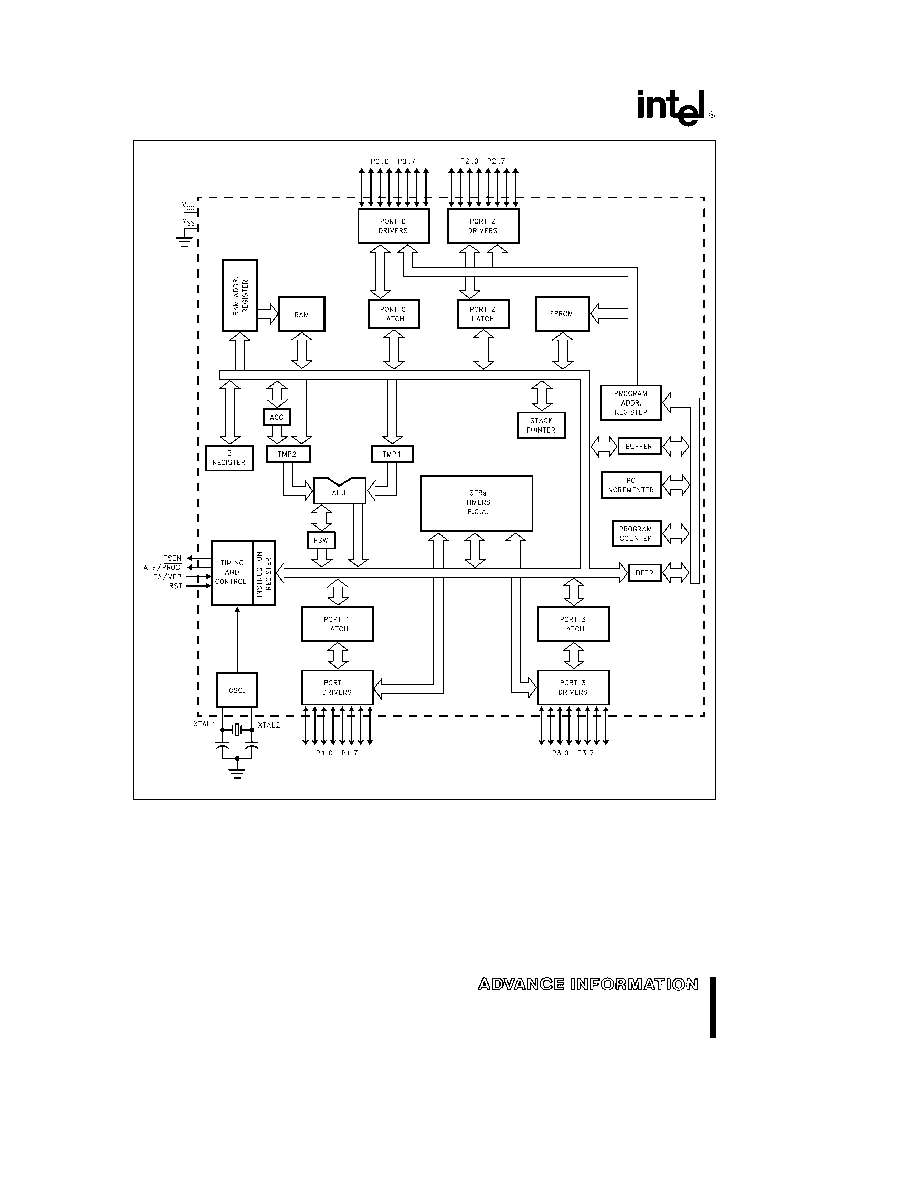
270961 � 1
Figure 1 87C51FB FC Block Diagram
87C51FA FB FC PRODUCT OPTIONS
Intel's extended and automotive temperature range
products are designed to meet the needs of those
applications whose operating requirements exceed
commercial standards
With the commercial standard temperature range
operational characteristics are guaranteed over the
temperature range of 0 C to 70 C ambient With the
extended temperature range option
operational
characteristics are guaranteed over the temperature
2
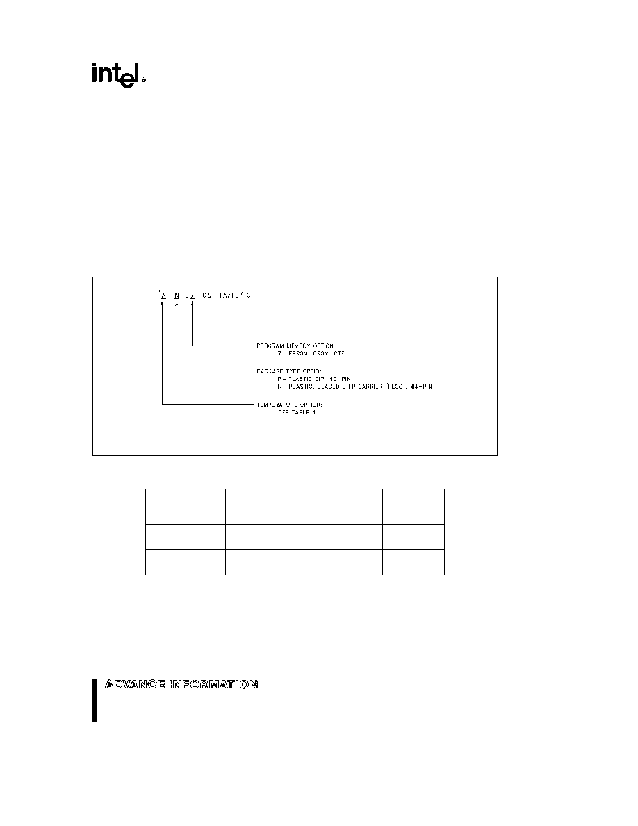
AUTOMOTIVE 87C51FA FB FC FC-20
range of b40 C to a85 C ambient For the automo-
tive temperature range option operational charac-
teristics are guaranteed over the temperature range
of b40 C to a125 C ambient The automotive ex-
tended and commercial temperature versions of the
MCS-51 product families are available with or with-
out burn-in options
As shown in Figure 2 temperature burn-in and
package options are identified by a one- or two-letter
prefix to the part number
PIN DESCRIPTIONS
V
CC
Supply voltage
V
SS
Circuit ground
V
SS1
Secondary ground (in PLCC only) Provided to
reduce ground bounce and improve power supply
by-passing
NOTE
This pin is NOT a substitute for V
SS
pin (pin 22)
Port 0
Port 0 is an 8-bit open drain bidirectional
I O port As an output port each pin can sink several
LS TTL inputs Port 0 pins that have 1's written to
them float and in that state can be used as high-im-
pedance inputs
270961 � 2
Example
AN87C51FA FB FC indicates an automotive temperature range version of the 87C51FA FB FC in a PLCC package
with 16 Kbyte 32 Kbyte EPROM program memory
Figure 2 Package Options
Table 1 Temperature Options
Temperature
Temperature
Operating
Burn-In
Classification
Designation
Temperature
Options
C Ambient
Extended
T
b
40 to a85
Standard
L
b
40 to a85
Extended
Automotive
A
b
40 to a125
Standard
B
b
40 to a125
Extended
3
AUTOMOTIVE 87C51FA FB FC FC-20
Port 0 is also the multiplexed low-order address and
data bus during accesses to external Program and
Data Memory In this application it uses strong inter-
nal pullups when emitting 1's and can source and
sink several LS TTL inputs
Port 0 also receives the code bytes during EPROM
programming and outputs the code bytes during
program verification External pullup resistors are re-
quired during program verification
Port 1
Port 1 is an 8-bit bidirectional I O port with
internal pullups The Port 1 output buffers can drive
LS TTL inputs Port 1 pins that have 1's written to
them are pulled high by the internal pullups and in
that state can be used as inputs As inputs Port 1
pins that are externally pulled low will source current
(I
IL
on the data sheet) because of the internal pull-
ups
In addition Port 1 serves the functions of the follow-
ing special features of the 87C51FB FC
Port Pin
Alternate Function
P1 0
T2 (External Count Input to
Timer Counter 2)
P1 1
T2EX (Timer Counter 2 Capture
Reload Trigger and Direction Control)
P1 2
ECI (External Count Input to the PCA)
P1 3
CEX0 (External I O for Compare
Capture Module 0)
P1 4
CEX1 (External I O for Compare
Capture Module 1)
P1 5
CEX2 (External I O for Compare
Capture Module 2)
P1 6
CEX3 (External I O for Compare
Capture Module 3)
P1 7
CEX4 (External I O for Compare
Capture Module 4)
Port 1 receives the low-order address bytes during
EPROM programming and verifying
Port 2
Port 2 is an 8-bit bidirectional I O port with
internal pullups The Port 2 output buffers can drive
LS TTL inputs Port 2 pins that have 1's written to
them are pulled high by the internal pullups and in
that state can be used as inputs As inputs Port 2
pins that are externally pulled low will source current
(I
IL
on the data sheet) because of the internal pull-
ups
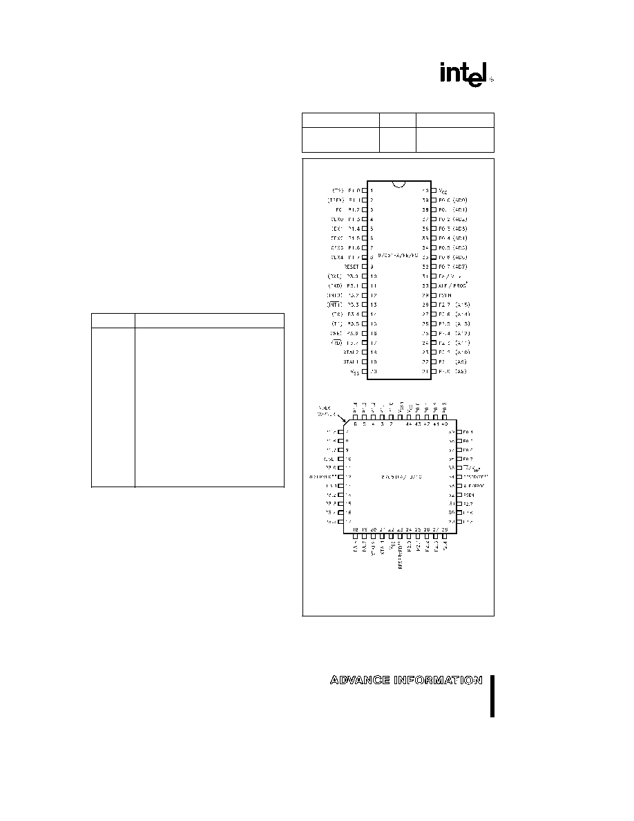
PACKAGES
Part
Prefix
Package Type
87C51FA FB FC
P
40-Pin Plastic DIP
N
44-Pin PLCC
DIP
270961 � 3
PAD (PLCC)
270961 � 4
EPROM only
Do not connect reserved pins
Diagrams are for pin reference only Package sizes are
not to scale
Figure 3 Pin Connections (Top View)
4

AUTOMOTIVE 87C51FA FB FC FC-20
Port 2 emits the high-order address byte during
fetches from external Program Memory and during
accesses to external Data Memory that use 16-bit
addresses (MOVX
DPTR) In this application it
uses strong internal pullups when emitting 1's Dur-
ing accesses to external Data Memory that use 8-bit
addresses (MOVX
Ri) Port 2 emits the contents
of the P2 Special Function Register
Some Port 2 pins receive the high-order address bits
during EPROM programming and program verifica-
tion
Port 3
Port 3 is an 8-bit bidirectional I O port with
internal pullups The Port 3 output buffers can drive
LS TTL inputs Port 3 pins that have 1's written to
them are pulled high by the internal pullups and in
that state can be used as inputs As inputs Port 3
pins that are externally pulled low will source current
(I
IL
on the data sheet) because of the pullups
Port 3 also serves the functions of various special
features of the MCS-51 Family as listed below
Port Pin
Alternate Function
P3 0
RXD (serial input port)
P3 1
TXD (serial output port)
P3 2
INT0 (external interrupt 0)
P3 3
INT1 (external interrupt 1)
P3 4
T0 (Timer 0 external input)
P3 5
T1 (Timer 1 external input)
P3 6
WR (external data memory write strobe)
P3 7
RD (external data memory read strobe)
RST
Reset input A high on this pin for two machine
cycles while the oscillator is running resets the de-
vice The port pins will be driven to their reset condi-
tion when a minimum V
IH1
is applied whether the
oscillator is running or not An internal pulldown re-
sistor permits a power-on reset with only a capacitor
connected to V
CC
ALE PROG
Address Latch Enable output pulse for
latching the low byte of the address during accesses
to external memory This pin (ALE PROG) is also
the program pulse input during EPROM program-
ming for the 87C51FA FB FC
In normal operation ALE is emitted at a constant
rate of
the oscillator frequency and may be used
for external timing or clocking purposes Note how-
ever that one ALE pulse is skipped during each ac-
cess to external Data Memory
Throughout the remainder of this data sheet ALE
will refer to the signal coming out of the ALE PROG
pin and the pin will be referred to as the ALE PROG
pin
PSEN
Program Store Enable is the read strobe to
external Program Memory
When the 87C51FA FB FC is executing code from
external Program Memory PSEN is activated twice
each machine cycle except that two PSEN activa-
tions are skipped during each access to external
Data Memory
EA V
PP
External Access enable
EA must be
strapped to V
SS
in order to enable the device to
fetch code from external Program Memory locations
0000H to 0FFFFH Note however that if either of
the Program Lock bits are programmed EA will be
internally latched on reset
EA should be strapped to V
CC
for internal program
executions
This pin also receives the programming supply volt-
age (V
PP
) during EPROM programming
XTAL1
Input to the inverting oscillator amplifier
XTAL2
Output from the inverting oscillator amplifier
OSCILLATOR CHARACTERISTICS
XTAL1 and XTAL2 are the input and output respec-
tively of an inverting amplifier which can be config-
ured for use as an on-chip oscillator as shown in
Figure 4 Either a quartz crystal or ceramic resonator
may be used More detailed information concerning
the use of the on-chip oscillator is available in Appli-
cation Note AP-155 ``Oscillators for Microcontrol-
lers'' and in Application Note AP-486
``Oscillator
Design for Microcontrollers''
5