 | –≠–ª–µ–∫—Ç—Ä–æ–Ω–Ω—ã–π –∫–æ–º–ø–æ–Ω–µ–Ω—Ç: 9880 | –°–∫–∞—á–∞—Ç—å:  PDF PDF  ZIP ZIP |


Datasheet
3
Document #: 248987
Revision#: 003
Rev Date: 08/07/01
Advanced 10/100 Repeater with Integrated Management -- LXT9860/9880
Contents
1.0
Other Related Documents............................................................................................. 11
2.0
Pin Assignments and Signal Descriptions .................................................................. 12
3.0
Functional Description .................................................................................................. 31
3.1
Introduction.......................................................................................................... 31
3.2
Port Configuration ............................................................................................... 32
3.2.1
Auto-Negotiation..................................................................................... 32
3.2.2
Forced Operation ................................................................................... 33
3.2.3
Changing Port Speed - Forced............................................................... 33
3.2.4
Link Establishment and Port Connection ............................................... 33
3.2.5
MII Port Configuration ............................................................................ 33
3.3
Interface Descriptions.......................................................................................... 33
3.3.1
Twisted-Pair Interface ............................................................................ 33
3.3.2
Media Independent Interface.................................................................. 34
3.3.3
Serial Management Interface ................................................................. 34
3.3.4
Serial PROM Interface ........................................................................... 35
3.4
Repeater Operation............................................................................................. 35
3.4.1
100 Mbps Repeater Operation ............................................................... 35
3.4.2
10 Mbps Repeater Operation ................................................................. 36
3.5
Management Support.......................................................................................... 37
3.5.1
Configuration and Status........................................................................ 37
3.5.2
SNMP and RMON Support .................................................................... 37
3.5.3
Source Address Management................................................................ 37
3.6
Requirements ...................................................................................................... 37
3.6.1
Power ..................................................................................................... 37
3.6.2
Clock ...................................................................................................... 38
3.6.3
Bias Resistor .......................................................................................... 38
3.6.4
Reset ...................................................................................................... 38
3.6.5
PROM..................................................................................................... 38
3.6.6
Chip ID ................................................................................................... 38
3.6.7
Management Master I/O Link ................................................................. 38
3.6.8
IRB Bus Pull-ups .................................................................................... 38
3.7
LED Operation..................................................................................................... 39
3.7.1
LEDs at Start-up..................................................................................... 39
3.7.2
LED Event Stretching ............................................................................. 39
3.7.3
LED Blink Rates ..................................................................................... 39
3.7.4
Serial LED Interface ............................................................................... 40
3.7.4.1 Serial Shifting ............................................................................ 40
3.7.4.2 Serial LED Signals .................................................................... 40
3.7.4.3 Activity Graph LEDs .................................................................. 41
3.7.5
Direct Drive LEDs................................................................................... 42
3.7.6
LED Modes............................................................................................. 42
3.7.6.1 LED Mode 1 .............................................................................. 44
3.7.6.2 LED Mode 2 .............................................................................. 45
3.7.6.3 LED Mode 3 .............................................................................. 46
3.7.6.4 LED Mode 4 .............................................................................. 47

LXT9860/9880 -- Advanced 10/100 Repeater with Integrated Management
4
Datasheet
Document #: 248987
Revision#: 003
Rev Date: 08/07/01
3.8
IRB Operation ..................................................................................................... 47
3.8.1
IRB Signal Types ................................................................................... 48
3.8.2
IRB Isolation ........................................................................................... 48
3.8.3
10 Mbps-Only Operation ........................................................................ 48
3.8.3.1 MAC IRB Access....................................................................... 48
3.8.3.2 Management Master Chain Arbitration...................................... 48
3.8.4
LXT98x/91x/98x0 Compatibility.............................................................. 48
3.9
MII Port Operation ............................................................................................... 51
3.9.1
Preamble Handling................................................................................. 51
3.10
Serial Management I/F ........................................................................................ 52
3.10.1 SMI Signals ............................................................................................ 52
3.10.1.1Serial Clock ............................................................................... 53
3.10.1.2Serial Data I/O........................................................................... 53
3.10.2 Read and Write Operations.................................................................... 53
3.10.2.1SMI Collision Handling .............................................................. 53
3.10.2.2SMI Address Match Indication .................................................. 53
3.10.2.3SMI Frame Format .................................................................... 54
3.10.3 Address Assignment Methods ............................................................... 57
3.10.3.1Chain Arbitration Mechanism .................................................... 58
3.10.3.2PROM Arbitration Mechanism................................................... 58
3.10.3.3Address Re-Arbitration .............................................................. 59
3.10.4 Interrupt Functions ................................................................................. 59
3.11
Serial PROM Interface ........................................................................................ 59
3.12
Serial Configuration Interface.............................................................................. 60
4.0
Application Information ................................................................................................. 61
4.1
General Design Guidelines ................................................................................. 61
4.2
Typical Applications ............................................................................................ 62
4.3
Application Circuitry ............................................................................................ 63
4.3.1
Power and Ground ................................................................................. 63
4.3.1.1 Supply Filtering.......................................................................... 63
4.3.1.2 Ground Noise ............................................................................ 63
4.3.1.3 Power and Ground Plane Layout Considerations ..................... 63
4.3.1.4 Chassis Ground......................................................................... 64
4.3.1.5 The RBIAS Pin .......................................................................... 64
4.3.2
MII Terminations .................................................................................... 65
4.3.3
Twisted-Pair Interface ............................................................................ 65
4.3.3.1 Magnetics Information ............................................................... 66
4.3.4
Clock ...................................................................................................... 66
4.3.5
SMI and PROM Circuits ......................................................................... 68
4.3.6
LED Circuits ........................................................................................... 69
4.3.6.1 Direct Drive LEDs...................................................................... 69
4.3.6.2 LED Pins Multiplexed with Configuration Inputs........................ 69
4.3.6.3 Serial LEDs ............................................................................... 70
4.4
Inter-Repeater Backplane Compatibility.............................................................. 71
4.4.1
Local Backplane--3.3V Only ................................................................. 72
4.4.2
Stack Backplane--3.3V or 5V ................................................................ 72
4.4.2.1 3.3V and 5.0V Stacking Boards Cannot Be Mixed.................... 72

Datasheet
5
Document #: 248987
Revision#: 003
Rev Date: 08/07/01
Advanced 10/100 Repeater with Integrated Management -- LXT9860/9880
5.0
Test Specifications......................................................................................................... 75
6.0
Register Definitions ....................................................................................................... 87
6.1
Register Map ....................................................................................................... 87
6.2
Counter Registers ............................................................................................... 95
6.2.1
Port Counter Registers........................................................................... 95
6.2.2
RMON Counter Registers ...................................................................... 96
6.3
Ethernet Address Registers ................................................................................ 99
6.3.1
Port Address Registers .......................................................................... 99
6.3.2
Search Address Registers...................................................................... 99
6.4
Repeater Port Control Registers .......................................................................101
6.4.1
General Port Control Registers ............................................................101
6.4.2
Port Link Control Register ....................................................................101
6.4.3
Port Learn Enable Register ..................................................................102
6.5
Repeater Port Status Registers.........................................................................102
6.6
PHY Port Status Registers ................................................................................104
6.7
PHY Port Control Registers...............................................................................107
6.8
Repeater Port Control/Status Registers ............................................................108
6.8.1
Device/Revision Register .....................................................................111
6.8.2
LED Control Registers.......................................................................... 111
6.8.3
LED Global Control Register ................................................................ 111
6.8.4
Port LED Control Register ....................................................................111
6.8.5
LED Timer Control Register .................................................................112
6.8.6
Repeater Reset Register......................................................................113
6.8.7
Software Reset Register ......................................................................113
6.8.8
Interrupt Registers................................................................................113
6.9
Serial Controller Registers ................................................................................115
7.0
Mechanical Specifications...........................................................................................117

LXT9860/9880 -- Advanced 10/100 Repeater with Integrated Management
6
Datasheet
Document #: 248987
Revision#: 003
Rev Date: 08/07/01
Figures
1
LXT98x0 Block Diagram ..................................................................................... 11
2
LXT98x0 Pin Assignments .................................................................................. 12
3
Typical LXT988x Managed Repeater Architectures ........................................... 32
4
MII Interface ........................................................................................................ 34
5
LED Blink Rates .................................................................................................. 39
6
Serial LED Shift Loading .................................................................................... 40
7
Serial LED Port Signaling.................................................................................... 41
8
100 Mbps IRB Connection .................................................................................. 49
9
IRB Block Diagram ............................................................................................. 50
10
LXT9880 MII Operation ....................................................................................... 52
11
Typical SMI Bus Architecture ............................................................................. 52
12
SMI Collision Handling ........................................................................................ 54
13
SMI Address Match Indication ............................................................................ 54
14
Serial Management Frame Format ..................................................................... 55
15
Address Arbitration Mechanisms ....................................................................... 58
16
Optional R/W Serial PROM Interface .................................................................. 60
17
Serial Configuration Interface.............................................................................. 61
18
Serial Configuration Interface Signaling .............................................................. 61
19
8-Port Managed 10/100 Stackable Repeater ...................................................... 62
20
32-Port Managed 10/100 Repeater..................................................................... 62
21
Power and Ground Connections ......................................................................... 65
22
Typical Twisted-Pair Port Interface and Power Supply Filtering ........................ 67
23
Typical Serial Management Interface Connections............................................. 68
24
Serial Controller Connection Showing PAL......................................................... 68
25
Serial PROM Interface ........................................................................................ 69
26
Typical Reset Circuit .......................................................................................... 69
27
LED Circuits - Direct Drive & Multiplexed Configuration Inputs .......................... 70
28
Serial LED Circuit................................................................................................ 71
29
100 Mbps Backplane Connection between LXT98x and LXT98x0 ..................... 73
30
Typical 100 Mbps IRB Implementation ............................................................... 74
31
Typical 10 Mbps IRB Implementation ................................................................ 74
32
100 Mbps TP Port-to-Port Delay Timing ............................................................. 79
33
100BASE-TX MII-to-TP Port Timing ................................................................... 80
34
100BASE-TX TP-to-MII Timing ........................................................................... 81
35
10BASE-T MII-to-TP Timing ............................................................................... 82
36
10BASE-T TP-to-MII Timing ............................................................................... 83
37
100 Mbps TP-to-IRB Timing................................................................................ 84
38
10 Mbps TP-to-IRB Timing.................................................................................. 84
39
10 Mbps IRB-to-TP Port Timing .......................................................................... 85
40
Serial Management Interface Timing .................................................................. 86
41
PROM Interface Timing....................................................................................... 87
42
LXT98x0 Package Specifications for Commercial Temperature....................... 117
43
LXT98x0 Package Specifications for Extended Temperature........................... 118

Datasheet
7
Document #: 248987
Revision#: 003
Rev Date: 08/07/01
Advanced 10/100 Repeater with Integrated Management -- LXT9860/9880
Tables
1
Signal Types........................................................................................................ 13
2
LXT98x0 Pins, Numeric Order ............................................................................ 13
3
MII #1 Signal Descriptions................................................................................... 20
4
MII #2 Signal Descriptions................................................................................... 21
5
Inter-Repeater Backplane Signal Descriptions.................................................... 22
6
Twisted-Pair Port Signal Descriptions ................................................................. 25
7
Serial Management Interface Signal Descriptions .............................................. 26
8
LED Signal Descriptions...................................................................................... 27
9
Power Supply and Indication Signal Descriptions ............................................... 28
10
PROM Interface Signal Descriptions................................................................... 29
11
Miscellaneous Signal Descriptions...................................................................... 30
12
Serial LED Port Bit Stream.................................................................................. 41
13
ACTGLED Display Modes................................................................................... 42
14
LED Terms .......................................................................................................... 43
15
LED Mode 1 Indications ...................................................................................... 44
16
LED Mode 2 Indications ...................................................................................... 45
17
LED Mode 3 Indications ...................................................................................... 46
18
LED Mode 4 Indications ...................................................................................... 47
19
Cascading and Stacking Connections................................................................. 50
20
IRB Signal Details ............................................................................................... 51
21
SMI Message Fields............................................................................................ 55
22
SMI Header Storage............................................................................................ 55
23
SMI Command Set .............................................................................................. 56
24
Typical Serial Management Packets ................................................................... 57
25
LXT98x0 Magnetics Specifications ..................................................................... 66
26
Oscillator Manufacturers ..................................................................................... 67
27
Absolute Maximum Ratings................................................................................. 75
28
Operating Conditions........................................................................................... 75
29
Input System Clock1 Requirements .................................................................... 75
30
I/O Electrical Characteristics ............................................................................... 76
31
100 Mbps IRB Electrical Characteristics ............................................................. 76
32
10 Mbps IRB Electrical Characteristics ............................................................... 77
33
100BASE-TX Transceiver Electrical Characteristics........................................... 78
34
10BASE-T Transceiver Electrical Characteristics ............................................... 78
35
100 Mbps TP Port-to-Port Delay Timing Parameters.......................................... 79
36
100BASE-TX MII-to-TP Port Timing Parameters ................................................ 80
37
100BASE-TX TP-to-MII Timing Parameters........................................................ 81
38
10BASE-T MII-to-TP Timing Parameters ............................................................ 82
39
10BASE-T TP-to-MII Timing Parameters ............................................................ 83
40
100 Mbps TP-to-IRB Timing Parameters
1 ................................................................................84
41
10 Mbps TP-to-IRB Timing Parameters
1...................................................................................85
42
10 Mbps IRB-to-TP Port Timing Parameters....................................................... 86
43
Serial Management Interface Timing Characteristics.......................................... 86
44
PROM Interface Timing Characteristics .............................................................. 87
45
Register Map ....................................................................................................... 88
46
Port Counter Registers........................................................................................ 95
47
RMON Counter Registers - 10 Mbps .................................................................. 97
48
RMON Counter Registers - 100 Mbps ................................................................ 98
49
Ethernet Address Register Bit Assignments ....................................................... 99

LXT9860/9880 -- Advanced 10/100 Repeater with Integrated Management
8
Datasheet
Document #: 248987
Revision#: 003
Rev Date: 08/07/01
50
Port Address Tracking Registers ........................................................................ 99
51
Search Address/Search Address Match Register ............................................. 100
52
Search Address Register Bit Assignments ....................................................... 100
53
Search Match Address Bit Assignments ........................................................... 100
54
Search Match Address Bit Definitions............................................................... 100
55
Port Control Register Bit Assignments .............................................................. 101
56
General Port Control Registers ......................................................................... 101
57
Port Link Control and Status Register Bit Assignments .................................... 101
58
Port Link Control Register ................................................................................. 102
59
Port Learn Enable Register ............................................................................... 102
60
Port Learn Enable Register ............................................................................... 102
61
Port Status Register Bit Assignments ............................................................... 103
62
Port Status Registers ........................................................................................ 103
63
MII Speed Status Bit Assignments .................................................................... 103
64
MII Status Bit Definitions ................................................................................... 103
65
Auto-Negotiation Registers ............................................................................... 104
66
Auto-Negotiate Link Partner Advertisement Bit Definitions............................... 104
67
Auto-Negotiate Expansion Bit Definitions ......................................................... 105
68
PHY Port Status Register Summary ................................................................. 105
69
PHY Port Status Register Bit Definitions........................................................... 106
70
Auto-Negotiation Advertisement Registers ....................................................... 107
71
Auto Negotiate Advertisement Bit Definitions ................................................... 107
72
PHY Port Control Register ................................................................................ 107
73
PHY Port Control Bit Definitions........................................................................ 108
74
Configuration Registers..................................................................................... 108
75
Repeater Configuration Register....................................................................... 109
76
Repeater Serial Configuration ........................................................................... 110
77
Device/Revision Register Bit Assignment ......................................................... 111
78
Global Fault LED Bit Assignments .................................................................... 111
79
.......................................................................................................................... 111
80
LED Configuration ............................................................................................. 112
81
Port LED1, 2, 3 Control Encodings ................................................................... 112
82
LED Timer Control Register Bit Assignments ................................................... 112
83
Repeater Reset ................................................................................................. 113
84
Software Reset.................................................................................................. 113
85
Interrupt Status/Mask Register.......................................................................... 113
86
Interrupt Status Register Bit Definitions ............................................................ 114
87
Interrupt Mask Bit Definitions ............................................................................ 115
88
Configuration Registers..................................................................................... 115
89
Assign Addr 1 .................................................................................................... 115
90
Assign Addr 2 .................................................................................................... 116
91
PROM Addr 1 .................................................................................................... 116
92
PROM Addr 2 .................................................................................................... 116

Datasheet
9
Document #: 248987
Revision#: 003
Rev Date: 08/07/01
Advanced 10/100 Repeater with Integrated Management -- LXT9860/9880
Revision History
Date
Revision
Page
Description
August 2001
003
75
Changed Absolute Maximum Ratings Supply Voltage value to 4.0V.
January 2001
002
Title Page
Added extended temperature range to title page.
13
Modified LXT98x0 Pins, Numeric Order table (Pins 10, 11, 17, 19, 20,
185.
38
Modified clock requirements language.
38
Replaced TBD with 3.15V under Reset.
65
Under Twisted Pair Interface, 4th bullet: Replaced text containingT-
BDs with: A ferrite bead with a total maximum current rating of
1.5Amp is recommended.
67
Modified Oscillator Manufacturers table.
75
Modified Absolute Maximum Ratings table.
75
Modified Operating Conditions table.
117
,
118
Mechanical Specifications: Add part number LXT98x0AHC to
LXT98x0 Package Specifications Commercial Temperature figure;
Add page for LXT98x0 Package Specifications Extended Tempera-
ture figure.


Advanced 10/100 Repeater with Integrated Management -- LXT9860/9880
Datasheet
Document #: 248987
Revision#: 003
Rev Date: 08/07/01
11
1.0
Other Related Documents...
The LXT98x0 Design and Layout Guide (formerly Application Note 113) provides detailed design
and layout guidelines.
The IRB Design and Layout Guide (formerly Application Note 112) provides detailed guidelines
design and layout of Intel's Inter-Repeater Backplane (IRB).
The LXT98x-to-LXT98x0 Migration Guide (formerly Application Note 111) compares features and
registers of the LXT98x and more recent LXT98x0 devices.
The LXT9883/LXT9863 Data Sheet specifically details the unmanaged eight-port and six-port
devices.
The High-Speed Serial Management Interface (formerly Application Note 64) explains how to
connect an SCC to Intel devices and how to implement management across a network system.
Figure 1. LXT98x0 Block Diagram
10BASE-T
Repeater
100BASE-X
Repeater
Serial LED
Drivers
10/100 PHY 1
RMON &
SNMP
Counters
10 Mbps
Backplane
100 Mbps
Backplane
Serial Port
Device
Management
P
o
rt
S
w
i
t
c
h
i
n
g
L
ogi
c
10M IRB
100M IRB
Mode Control
Serial Mgmt
Port & Mgmt
Status Indicators
TX_I/O
10/100 PHY 2
TX_I/O
10/100 PHY 3
TX_I/O
10/100 PHY 4
TX_I/O
10/100 PHY 5
TX_I/O
10/100 PHY 6
TX_I/O
10/100 PHY 7
TX_I/O
10/100 PHY 8
TX_I/O
MII 1
MII_I/O
MII 2
MII_I/O

LXT9860/9880 -- Advanced 10/100 Repeater with Integrated Management
12
Datasheet
Document #: 248987
Revision#: 003
Rev Date: 08/07/01
2.0
Pin Assignments and Signal Descriptions
Figure 2. LXT98x0 Pin Assignments
RESET ....... 53
CLK25 ....... 54
IR10ISO ....... 55
IR100ISO ....... 56
RECONFIG ....... 57
SRX ....... 58
STX ....... 59
SERCLK ....... 60
VCC ....... 61
GND ....... 62
SER_MATCH ....... 63
MMSTROUT ....... 64
ARBOUT ....... 65
N/C ....... 66
MGR_PRES ....... 67
PROM_CLK ....... 68
PROM_CS ....... 69
PROM_DTOUT ....... 70
PROM_DTIN ....... 71
CHIPID0 ....... 72
CHIPID1 ....... 73
VCC ....... 74
GND ....... 75
VCC ....... 76
VCC ....... 77
RPS_FAULT ....... 78
RPS_PRES ....... 79
MACACTIVE ....... 80
HOLDCOL ....... 81
LEDCLK/CFG_CLK ... 82
LEDDAT ....... 83
LEDLAT ....... 84
VCC ....... 85
GND ....... 86
PORT1_LED3 ....... 87
PORT1_LED2 ....... 88
PORT1_LED1 ....... 89
GND ....... 90
PORT2_LED3 ....... 91
PORT2_LED2 ....... 92
PORT2_LED1 ....... 93
GND ....... 94
PORT3_LED3 ....... 95
PORT3_LED2 ....... 96
PORT3_LED1 ....... 97
GND ....... 98
PORT4_LED3 ....... 99
PORT4_LED2 ....... 100
PORT4_LED1 ....... 101
RBIAS ....... 102
GND ....... 103
TPIP1 ....... 104
208........MII2_RXD3
207........MII2_RXD2
206........MII2_RXD1
205........MII2_RXD0
204........MII2_RXDV
203........MII2_RXCLK
202........MII2_RXER
201........MMSTRIN
200........VCC
199........GND
198........ARBIN
197........MII2_TXER
196........MII2_TXCLK
195........MII2_TXEN
194........MII2_TXD0
193........MII2_TXD1
192........MII2_TXD2
191........MII2_TXD3
190........VCC
189........GND
188........MII2_COL
187........MII2_CRS
186........ARBSELECT/COL100_LED
185........LEDSEL1/COL10_LED
184........LEDSEL0/ACT100_LED
183........ AUTOBLINK/ACT10_LED
182........ IRQ
181........GND
180........VCC
179........GND
178........N/C
177........VCC
176........PORT8_LED1*
175........PORT8_LED2*/LEDABGSEL
174......... PORT8_LED3*
173........VCC
172........GND
171........PORT7_LED1*
170........PORT7_LED2*
169........PORT7_LED3*
168........GND
167........PORT6_LED1
166........PORT6_LED2
165........PORT6_LED3
164........GND
163........PORT5_LED1
162........PORT5_LED2
161........PORT5_LED3
160........TxSLEW_1
159........TxSLEW_0
158......... GND
157........*TPIP8
TP
IN
1
....
...
1
0
5
V
C
C
R
....
...
1
0
6
TP
OP
1
....
...
1
0
7
TP
ON
1
....
...
1
0
8
GN
D
....
...
1
0
9
TP
ON
2
....
...
1
1
0
TP
OP
2
....
...
1
1
1
V
C
C
T
....
...
1
1
2
V
C
C
R
....
...
1
1
3
TP
IN
2
....
...
1
1
4
TP
IP
2
....
...
1
1
5
GN
D
....
...
1
1
6
GN
D
....
...
1
1
7
TP
IP
3
....
...
1
1
8
TP
IN
3
....
...
1
1
9
V
C
C
R
....
...
1
2
0
TP
OP
3
....
...
1
2
1
TP
ON
3
....
...
1
2
2
GN
D
....
...
1
2
3
TP
ON
4
....
...
1
2
4
TP
OP
4
....
...
1
2
5
V
C
C
T
....
...
1
2
6
V
C
C
R
....
...
1
2
7
TP
IN
4
....
...
1
2
8
TP
IP
4
....
...
1
2
9
GN
D
....
...
1
3
0
GN
D
....
...
1
3
1
TP
IP
5
....
...
1
3
2
TP
IN
5
....
...
1
3
3
V
C
C
R
....
...
1
3
4
V
C
C
T
....
...
1
3
5
TP
OP
5
....
...
1
3
6
TP
ON
5
....
...
1
3
7
GN
D
....
...
1
3
8
TP
ON
6
....
...
1
3
9
TP
OP
6
....
...
1
4
0
V
C
C
R
....
...
1
4
1
TP
IN
6
....
...
1
4
2
TP
IP
6
....
...
1
4
3
GN
D
....
...
1
4
4
GN
D
....
...
1
4
5
*
TP
IP
7
....
...
1
4
6
*
TP
IN
7
....
...
1
4
7
V
C
C
R
....
...
1
4
8
V
C
C
T
....
...
1
4
9
*
TP
OP
7
....
...
1
5
0
*
TP
ON
7
....
...
1
5
1
GN
D
....
...
1
5
2
*
TP
ON
8
....
...
1
5
3
*
TP
OP
8
....
...
1
5
4
V
C
C
R
....
...
1
5
5
*
TP
IN
8
....
...
1
5
6
* Indicates LXT9880-only pins. TP Ports 7 and 8 are not available on LXT9860 devices.
5
2
.....
.....
N
C
5
1
.....
.....
N
C
5
0
.....
.....
IR
1
0
0
C
L
K
4
9
.....
.....
IR
1
0
0
D
A
T4
4
8
.....
.....
IR
1
0
0
D
A
T3
4
7
.....
.....
V
C
C
4
6
.....
.....
GN
D
4
5
.....
.....
IR
1
0
0
D
A
T2
4
4
.....
.....
IR
1
0
0
D
A
T1
4
3
.....
.....
IR
1
0
0
D
A
T0
4
2
.....
.....
I
R
1
0
0
D
V
4
1
.....
.....
I
R
1
0
0
D
E
N
4
0
.....
.....
I
R
1
0
0
C
O
L
3
9
.....
.....
C
O
M
P
_
S
E
L
3
8
.....
.....
I
R
1
0
0
S
N
G
L
3
7
.....
.....
I
R
1
0
0
C
F
S
B
P
3
6
.....
.....
I
R
1
0
0
C
F
S
3
5
.....
.....
M
II1
_
R
X
D
3
3
4
.....
.....
M
II1
_
R
X
D
2
3
3
.....
.....
C
O
N
F
IG0
/
C
F
G_
D
T
3
2
....
.....
M
II1
_
R
X
D
1
3
1
.....
.....
M
II1
_
R
X
D
0
3
0
.....
.....
M
II1
_
R
X
D
V
2
9
.....
.....
M
II1
_
R
X
C
L
K
2
8
.....
.....
V
C
C
2
7
.....
.....
GN
D
2
6
.....
.....
M
II1
_
R
X
E
R
2
5
.....
.....
C
O
N
F
IG1
/
C
F
G_
L
D
2
4
.....
.....
M
II1
_
T
X
E
R
2
3
.....
.....
M
II1
_
T
X
C
L
K
2
2
.....
.....
M
II1
_
T
X
E
N
2
1
.....
.....
M
II1
_
T
X
D
0
2
0
.....
.....
M
II1
_
T
X
D
1
1
9
.....
.....
M
II1
_
T
X
D
2
1
8
.....
.....
M
II2
_
S
P
D
1
7
.....
.....
M
II1
_
T
X
D
3
1
6
.....
.....
V
C
C
1
5
.....
.....
GN
D
1
4
.....
.....
M
II1
_
C
OL
1
3
.....
.....
M
II1
_
C
R
S
1
2
.....
.....
IR
1
0
C
L
K
1
1
.....
.....
IR
1
0
D
A
T
1
0
.....
.....
I
R
1
0
E
N
A
9
.
......
.....
M
II1
_
S
P
D
8
.
......
.....
V
C
C
7
.
......
.....
GN
D
6
.
......
.....
I
R
1
0
D
E
N
5
.
......
.....
I
R
1
0
C
FS
B
P
4
.
......
.....
I
R
1
0
C
OL
B
P
3
.
......
.....
I
R
1
0
C
OL
2
.
......
.....
I
R
1
0
C
FS
1
.
......
.....
GN
D
LXT98x0 XX
XXXXXX
XXXXXXXX
Part #
LOT #
FPO #
Rev #

Advanced 10/100 Repeater with Integrated Management -- LXT9860/9880
Datasheet
Document #: 248987
Revision#: 003
Rev Date: 08/07/01
13
Table 1. Signal Types
Type
Name
Definition
I
Input
Standard input-only signal.
O
Output
Standard output-only signal.
I/O
Bidirectional
Input and output signal.
A
Analog
Current source signal.
OD
Open Drain
Output that will only drive the signal Low.
OS
Open Source
Output that will only drive the signal High.
PD
Pull Down
Internal, weak pull down signal.
PU
Pull Up
Internal, weak pull up signal.
NC
No Clamp
Pad does not clamp input in the absence of power.
Table 2. LXT98x0 Pins, Numeric Order
Pin
Symbol
Type
1,2
Reference
for Full Description
1.
GND
-
Table 9 on page 28
2.
IR10CFS
A, I/O, OD
Table 5 on page 22
3.
IR10COL
I/O, OD, PU
Table 5 on page 22
4.
IR10COLBP I/O,
OD
Table 5 on page 22
5.
IR10CFSBP
A I/O, OD
Table 5 on page 22
6.
IR10DEN O,
OD
Table 5 on page 22
7.
GND
-
Table 9 on page 28
8.
VCC
-
Table 9 on page 28
9.
MII1_SPD
I, PU
Table 3 on page 20
10.
IR10ENA
O,
Table 3 on page 20
11.
IR10DAT
O
Table 3 on page 20
12.
IR10CLK
I/O
Table 5 on page 22
13.
MII1_CRS
O
Table 3 on page 20
14.
MII1_COL
O
Table 3 on page 20
15.
GND
-
Table 9 on page 28
16.
VCC
-
Table 9 on page 28
17.
MII1_TXD3
I
Table 3 on page 20
18.
MII2_SPD
I
Table 3 on page 20
19.
MII1_TXD2
I
Table 3 on page 20
20.
MII1_TXD1
I
Table 3 on page 20
21.
MII1_TXD0
I
Table 3 on page 20
1. Refer to
Table 1
for Signal Type definitions.
2. Pins are 5V tolerant, unless indicated.
3. Input must be static; Refer to
"LED Pins Multiplexed with
Configuration Inputs" on page 69
for information on pin use.

LXT9860/9880 -- Advanced 10/100 Repeater with Integrated Management
14
Datasheet
Document #: 248987
Revision#: 003
Rev Date: 08/07/01
22.
MII1_TXEN
I
Table 3 on page 20
23.
MII1_TXCLK
I
Table 3 on page 20
24.
MII1_TXER
I
Table 3 on page 20
25.
CONFIG1/CF
I/O
Table 11 on page 30
26.
MII1RXER
I
Table 3 on page 20
27.
GND
-
Table 9 on page 28
28.
VCC
-
Table 9 on page 28
29.
MII1_RXCLK
O
Table 3 on page 20
30.
MII1_RXDV
O
Table 3 on page 20
31.
MII1_RXD0
O
Table 3 on page 20
32.
MII1_RXD1
O
Table 3 on page 20
33.
CONFIG/CFG_DT
I
Table 12 on page 41
34.
MII1_RXD2
O
Table 3 on page 20
35.
MII1_RXD3
O
Table 3 on page 20
36.
IR100CFS A
I/O
Table 5 on page 22
37.
IR100CFSBP A
I/O
Table 5 on page 22
38.
IR100SNGL I/O
Table 5 on page 22
39.
COMP_SEL
AI
Table 5 on page 22
40.
IR100COL
O
Table 5 on page 22
41.
IR100DEN
O
Table 5 on page 22
42.
IR100DV I/O
Table 5 on page 22
43.
IR100DAT0
I/O
Table 5 on page 22
44.
IR100DAT1
I/O
Table 5 on page 22
45.
IR100DAT2
I/O
Table 5 on page 22
46.
GND
-
Table 9 on page 28
47.
VCC
-
Table 9 on page 28
48.
IR100DAT3
I/O
Table 5 on page 22
49.
IR100DAT4
I/O
Table 5 on page 22
50.
IR100CLK
I/O
Table 5 on page 22
51.
NC
-
Table 11 on page 30
52.
NC
-
Table 11 on page 30
53.
RESET
I
Table 11 on page 30
54.
CLK25
I
Table 11 on page 30
55.
IR10ISO
O
Table 5 on page 22
Table 2. LXT98x0 Pins, Numeric Order
Pin
Symbol
Type
1,2
Reference
for Full Description
1. Refer to
Table 1
for Signal Type definitions.
2. Pins are 5V tolerant, unless indicated.
3. Input must be static; Refer to
"LED Pins Multiplexed with
Configuration Inputs" on page 69
for information on pin use.

Advanced 10/100 Repeater with Integrated Management -- LXT9860/9880
Datasheet
Document #: 248987
Revision#: 003
Rev Date: 08/07/01
15
56.
IR100ISO
O
Table 5 on page 22
57.
RECONFIG
I, PD
Table 7 on page 26
58.
SRX
I, PD
Table 7 on page 26
59.
STX
O, OD
Table 7 on page 26
60.
SERCLK
I/O, Tri-State,
PD
Table 7 on page 26
61. VCC
-
Table 9 on page 28
62.
GND
Table 9 on page 28
63.
SER_MATCH
O
Table 7 on page 26
64.
MMSTROUT
O
Table 5 on page 22
65.
ARBOUT
O
Table 7 on page 26
66. NC
-
Table 11 on page 30
67.
MGR_PRES
I
PU
Table 7 on page 26
68.
PROM_CLK
I/O
Tri-State
PD
Table 10 on page 29
69.
PROM_CS
O, Tri-State
Table 10 on page 29
70.
PROM_DTOUT
O, Tri-State
Table 10 on page 29
71.
PROM_DTIN
I, PD
Table 10 on page 29
72.
CHIPID0
I
PD
Table 11 on page 30
73.
CHIPID1
I
PD
Table 11 on page 30
74.
VCC
-
Table 9 on page 28
75.
GND
-
Table 9 on page 28
76.
VCC
-
Table 9 on page 28
77.
VCC
-
Table 9 on page 28
78.
RPS_FAULT I,
PU
Table 9 on page 28
79.
RPS_PRES
I, PU
Table 9 on page 28
80.
MACACTIVE
I, PD
Table 5 on page 22
81.
HOLDCOL
I/O, PD
Table 5 on page 22
82.
LEDCLK
CFG_CLK
O
Table 8 on page 27
83.
LEDDAT
O
Table 8 on page 27
84.
LEDLAT
O
Table 8 on page 27
85.
VCC
-
Table 9 on page 28
Table 2. LXT98x0 Pins, Numeric Order
Pin
Symbol
Type
1,2
Reference
for Full Description
1. Refer to
Table 1
for Signal Type definitions.
2. Pins are 5V tolerant, unless indicated.
3. Input must be static; Refer to
"LED Pins Multiplexed with
Configuration Inputs" on page 69
for information on pin use.

LXT9860/9880 -- Advanced 10/100 Repeater with Integrated Management
16
Datasheet
Document #: 248987
Revision#: 003
Rev Date: 08/07/01
86.
GND
-
Table 9 on page 28
87.
PORT1_LED3
O, OD
Table 8 on page 27
88.
PORT1_LED2
O, OD
Table 8 on page 27
89.
PORT1_LED1
O, OD
Table 8 on page 27
90.
GND
-
Table 9 on page 28
91.
PORT2_LED3
O, OD
Table 8 on page 27
92.
PORT2_LED2
O, OD
Table 8 on page 27
93.
PORT2_LED1
O, OD
Table 8 on page 27
94.
GND
-
Table 9 on page 28
95.
PORT3_LED3
O, OD
Table 8 on page 27
96.
PORT3_LED2
O, OD
Table 8 on page 27
97.
PORT3_LED1
O, OD
Table 8 on page 27
98.
GND
-
Table 9 on page 28
99.
PORT4_LED3
O, OD
Table 8 on page 27
100.
PORT4_LED2
O, OD
Table 8 on page 27
101.
PORT4_LED1
O, OD
Table 8 on page 27
102.
RBIAS
A
Table 9 on page 28
103.
GND
-
Table 9 on page 28
104.
TPIP1
AI
Table 6 on page 25
105.
TPIN1
AI
Table 6 on page 25
106.
VCCR
-
Table 9 on page 28
107.
TPOP1
AO
Table 6 on page 25
108.
TPON1
AO
Table 6 on page 25
109.
GND
-
Table 9 on page 28
110.
TPON2
AO
Table 6 on page 25
111.
TPOP2
AO
Table 6 on page 25
112.
VCCT
-
Table 9 on page 28
113.
VCCR
-
Table 9 on page 28
114.
TPIN2
AI
Table 6 on page 25
115.
TPIP2
AI
Table 6 on page 25
116.
GND
-
Table 9 on page 28
117.
GND
-
Table 9 on page 28
118.
TPIP3
AI
Table 6 on page 25
119.
TPIN3
AI
Table 6 on page 25
Table 2. LXT98x0 Pins, Numeric Order
Pin
Symbol
Type
1,2
Reference
for Full Description
1. Refer to
Table 1
for Signal Type definitions.
2. Pins are 5V tolerant, unless indicated.
3. Input must be static; Refer to
"LED Pins Multiplexed with
Configuration Inputs" on page 69
for information on pin use.

Advanced 10/100 Repeater with Integrated Management -- LXT9860/9880
Datasheet
Document #: 248987
Revision#: 003
Rev Date: 08/07/01
17
120.
VCCR
-
Table 9 on page 28
121.
TPOP3
AO
Table 6 on page 25
122.
TPON3
AO
Table 6 on page 25
123.
GND
-
Table 9 on page 28
124.
TPON4
AO
Table 6 on page 25
125.
TPOP4
AO
Table 6 on page 25
126.
VCCT
-
Table 9 on page 28
127.
VCCR
-
Table 9 on page 28
128.
TPIN4
AI
Table 6 on page 25
129.
TPIP4
AI
Table 6 on page 25
130.
GND
-
Table 9 on page 28
131.
GND
-
Table 9 on page 28
132.
TPIP5
AI
Table 6 on page 25
133.
TPIN5
AI
Table 6 on page 25
134.
VCCR
-
Table 9 on page 28
135.
VCCT
-
Table 9 on page 28
136.
TPOP5
AO
Table 6 on page 25
137.
TPON5
AO
Table 6 on page 25
138.
GND
-
Table 9 on page 28
139.
TPON6
AO
Table 6 on page 25
140.
TPOP6
AO
Table 6 on page 25
141.
VCCR
-
Table 9 on page 28
142.
TPIN6
AI
Table 6 on page 25
143.
TPIP6
AI
Table 6 on page 25
144.
GND
-
Table 9 on page 28
145.
GND
-
Table 9 on page 28
146.
TPIP7
AI
Table 6 on page 25
147.
TPIN7
AI
Table 6 on page 25
148.
VCCR
-
Table 9 on page 28
149.
VCCT
-
Table 9 on page 28
150.
TPOP7
AO
Table 6 on page 25
151.
TPON7
AO
Table 6 on page 25
152.
GND
-
Table 9 on page 28
153.
TPON8
AO
Table 6 on page 25
Table 2. LXT98x0 Pins, Numeric Order
Pin
Symbol
Type
1,2
Reference
for Full Description
1. Refer to
Table 1
for Signal Type definitions.
2. Pins are 5V tolerant, unless indicated.
3. Input must be static; Refer to
"LED Pins Multiplexed with
Configuration Inputs" on page 69
for information on pin use.

LXT9860/9880 -- Advanced 10/100 Repeater with Integrated Management
18
Datasheet
Document #: 248987
Revision#: 003
Rev Date: 08/07/01
154.
TPOP8
AO
Table 6 on page 25
155.
VCCR
-
Table 9 on page 28
156.
TPIN8
AI
Table 6 on page 25
157.
TPIP8
AI
Table 6 on page 25
158.
GND
-
Table 9 on page 28
159.
TxSLEW_0
I, PD
Table 6 on page 25
160.
TxSLEW_1
I, PD
Table 6 on page 25
161.
PORT5_LED3
O, OD
Table 8 on page 27
162.
PORT5_LED2
O, OD
Table 8 on page 27
163.
PORT5_LED1
O, OD
Table 8 on page 27
164.
GND
-
Table 9 on page 28
165.
PORT6_LED3
O, OD
Table 8 on page 27
166.
PORT6_LED2
O, OD
Table 8 on page 27
167.
PORT6_LED1
O, OD
Table 8 on page 27
168.
GND
-
Table 9 on page 28
169.
PORT7_LED3
O, OD
Table 8 on page 27
170.
PORT7_LED2
O, OD
Table 8 on page 27
171.
PORT7_LED1
O, OD
Table 8 on page 27
172.
GND
-
Table 9 on page 28
173.
VCC
-
Table 9 on page 28
174.
PORT8_LED3
O, OD
Table 8 on page 27
175.
PORT8_LED2
O, OD
Table 8 on page 27
LEDABGSEL
I
3
, O-OD/OS
Table 8 on page 27
176.
PORT8_LED1
O, OD
Table 8 on page 27
177.
VCC
-
Table 9 on page 28
178.
N/C
-
Table 11 on page 30
179.
GND
-
Table 9 on page 28
180.
VCC
-
Table 9 on page 28
181.
GND
-
Table 9 on page 28
182.
IRQ O,
OD
Table 11 on page 30
183.
AUTOBLINK/
I
3
, O-OD/OS
Table 8 on page 27
ACT10LED
I
3
, O-OD/OS
Table 8 on page 27
184.
LEDSEL0
I
3
, O-OD/OS
Table 8 on page 27
ACT_100_LED
I
3
, O-OD/OS
Table 8 on page 27
Table 2. LXT98x0 Pins, Numeric Order
Pin
Symbol
Type
1,2
Reference
for Full Description
1. Refer to
Table 1
for Signal Type definitions.
2. Pins are 5V tolerant, unless indicated.
3. Input must be static; Refer to
"LED Pins Multiplexed with
Configuration Inputs" on page 69
for information on pin use.

Advanced 10/100 Repeater with Integrated Management -- LXT9860/9880
Datasheet
Document #: 248987
Revision#: 003
Rev Date: 08/07/01
19
185.
LEDSEL1
I
3
, O-OD/OS
Table 8 on page 27
COL10_LED
I
3
, O-OD/OS
Table 8 on page 27
186.
ARBSELECT
I
3
, O-OD/OS
Table 7 on page 26
COL100_LED
I
3
, O-OD/OS
Table 8 on page 27
187.
MII2_CRS
O
Table 4 on page 21
188.
MII2_COL
O
Table 4 on page 21
189.
GND
-
Table 9 on page 28
190.
VCC
-
Table 9 on page 28
191.
MII2_TXD3
I
Table 4 on page 21
192.
MII2_TXD2
I
Table 4 on page 21
193.
MII2_TXD1
I
Table 4 on page 21
194.
MII2_TXD0
I
Table 4 on page 21
195.
MII2_TXEN
I
Table 4 on page 21
196.
MII2_TXCLK
O
Table 4 on page 21
197.
MII2_TXER
I
Table 4 on page 21
198.
ARBIN
I, PD
Table 7 on page 26
199.
GND
-
Table 9 on page 28
200.
VCC
-
Table 9 on page 28
201.
MMSTRIN
I, PD
Table 5 on page 22
202.
MII2_RXER
O
Table 4 on page 21
203.
MII2_RXCLK
O
Table 4 on page 21
204.
MII2_RXDV
O
Table 4 on page 21
205.
MII2_RXD0
O
Table 4 on page 21
206.
MII2_RXD1
O
Table 4 on page 21
207.
MII2_RXD2
O
Table 4 on page 21
208.
MII2_RXD3
O
Table 4 on page 21
Table 2. LXT98x0 Pins, Numeric Order
Pin
Symbol
Type
1,2
Reference
for Full Description
1. Refer to
Table 1
for Signal Type definitions.
2. Pins are 5V tolerant, unless indicated.
3. Input must be static; Refer to
"LED Pins Multiplexed with
Configuration Inputs" on page 69
for information on pin use.

LXT9860/9880 -- Advanced 10/100 Repeater with Integrated Management
20
Datasheet
Document #: 248987
Revision#: 003
Rev Date: 08/07/01
Table 3. MII #1 Signal Descriptions
Pin
Symbol
Type
1, 2
Description
9
MII1_SPD
I
PU
Speed Select - MII 1. This signal is sensed at power up,
hardware reset, and software reset. Selects operating speed of
the respective MII (MAC) interface.
High = 100 Mbps. Low = 10 Mbps.
31
32
34
35
MII1_RXD0
MII1_RXD1
MII1_RXD2
MII1_RXD3
O
Receive Data - MII 1. The LXT98x0 transmits received data to
the controller on these outputs. Data is driven on the falling edge
of MII1_RXCLK.
30
MII1_RXDV
O
Receive Data Valid - MII 1. Active High signal, synchronous to
MII1_RXCLK, indicates valid data on MII1_RXD<3:0>.
29
MII1_RXCLK
O
Receive Clock - MII 1. MII receive clock for expansion port. This
is a 2.5 or 25 MHz clock derived from the CLK25 input (refer to
Table 11 on page 30
).
26
MII1_RXER
O
Receive Error - MII 1. Active High signal, synchronous to
MII1_RXCLK, indicates invalid data on MII1_RXD<3:0>.
24
MII1_TXER
I
Transmit Error - MII 1. MII1_TXER is a 100 Mbps-only signal.
The MAC asserts this input when an error has occurred in the
transmit data stream. The LXT98x0 responds by sending `Invalid
Code Symbols' on the line.
23
MII1_TXCLK
O
Transmit Clock - MII 1. This is a 2.5 or 25 MHz clock derived
from the CLK25 input (refer to
Table 11 on page 30
).
22
MII1_TXEN
I
Transmit Enable - MII 1. External controllers drive this input High
to indicate data is transmitted on the MII1_TXD<3:0> pins.
Ground this input if unused.
21
20
19
17
MII1_TXD0
MII1_TXD1
MII1_TXD2
MII1_TXD3
I
Transmit Data - MII 1. External controllers use these inputs to
transmit data to the LXT98x0. The LXT98x0 samples
MII1_TXD<3:0> on the rising edge of MII1_TXCLK, when
MII1_TXEN is High.
14
MII1_COL
O
Collision - MII 1. The LXT98x0 drives this signal High to indicate
a collision occurred.
13
MII1_CRS
O
Carrier Sense - MII 1. Active High signal indicates LXT98x0 is
transmitting or receiving.
1. I = Input, O = Output, I/O = Input/Output, D = Digital, A = Analog, AI = Analog Input,
A I/O = Analog Input/Output, OD = Open Drain, OS = Open Source, PD = Pull Down, PU = Pull Up.
NC = No Clamp. Pad does not clamp input in the absence of power.
2. Pins are 5V tolerant, unless indicated.

Advanced 10/100 Repeater with Integrated Management -- LXT9860/9880
Datasheet
Document #: 248987
Revision#: 003
Rev Date: 08/07/01
21
Table 4. MII #2 Signal Descriptions
Pin
Symbol
Type
1, 2
Description
18
MII2_SPD
I
PU
Speed Select - MII 2. This signal is sensed at power up,
hardware reset, and software reset. Selects operating speed of
the respective MII (MAC) interface.
High = 100 Mbps. Low = 10 Mbps.
205
206
207
208
MII2_RXD0
MII2_RXD1
MII2_RXD2
MII2_RXD3
O
Receive Data - MII 2. The LXT98x0 transmits received data to
the controller on these outputs. Data is driven on the falling edge
of MII2_RXCLK.
204
MII2_RXDV
O
Receive Data Valid - MII 2. Active High signal, synchronous to
MII2_RXCLK, indicates valid data on MII2_RXD<3:0>.
203
MII2_RXCLK
O
Receive Clock - MII 2. MII receive clock for expansion port. This
is a 2.5 or 25 MHz clock derived from the CLK25 input (refer to
Table 11 on page 30
).
202
MII2_RXER
O
Receive Error - MII 2. Active High signal, synchronous to
MII2_RXCLK, indicates invalid data on MII2_RXD<3:0>.
197
MII2_TXER
I
Transmit Error - MII 2. MII2_TXER is a 100 Mbps-only signal.
The MAC asserts this input when errors occurs in the transmit
data stream. The LXT98x0 sends `Invalid Code Symbols' on the
line.
196
MII2_TXCLK
O
Transmit Clock - MII 2. This is a 2.5 or 25 MHz clock derived
from the CLK25 input (refer to
Table 11 on page 30
).
195
MII2_TXEN
I
Transmit Enable - MII 2. External controllers drive this input High
to indicate data is transmitted on the MII2_TXD<3:0> pins.
Ground this input if unused.
194
193
192
191
MII2_TXD0
MII2_TXD1
MII2_TXD2
MII2_TXD3
I
Transmit Data - MII 2. External controllers use these inputs to
transmit data to the LXT98x0. The LXT98x0 samples
MII2_TXD<3:0> on the rising edge of MII2_TXCLK, when
MII2_TXEN is High.
188
MII2_COL
O
Collision - MII 2. The LXT98x0 drives this signal High to indicate
a collision occurred.
187
MII2_CRS
O
Carrier Sense - MII 2. Active High signal indicates LXT98x0 is
transmitting or receiving.
1. I = Input, O = Output, I/O = Input/Output, D = Digital, A = Analog, AI = Analog Input,
A I/O = Analog Input/Output, OD = Open Drain, OS = Open Source, PD = Pull Down, PU = Pull Up.
NC = No Clamp. Pad does not clamp input in the absence of power.
2. Pins are 5V tolerant, unless indicated.

LXT9860/9880 -- Advanced 10/100 Repeater with Integrated Management
22
Datasheet
Document #: 248987
Revision#: 003
Rev Date: 08/07/01
Table 5. Inter-Repeater Backplane Signal Descriptions
Pin
Symbol
Type
1, 2
Description
Common IRB Signals
39
COMP_SEL
AI
Compatibility Mode Select. 3.3V on this pin causes the
IRCFSBP signals to operate in 3.3V only mode. 5V on this pin
causes the IR100CFSBP or IR10CFSBP signals to operate in 5V
backwards compatibility mode with legacy LXT98x and LXT91x
devices.
100 Mbps IRB Signals
36
IR100CFS
3
A I/O
OD
100 Mbps IRB Collision Force Sense. A three-level signal that
determines number of active ports on the "logical" repeater. High
level (3.3V) indicates no ports active; Mid level (approx. 1.6V)
indicates one port active; Low level (0V) indicates more than one
port active, resulting in a collision. This signal requires a 215
pull-up resistor, and connects between ICs on the same board.
37
IR100CFSBP
A I/O
OD
100 Mbps IRB Collision Force Sense - Backplane. This three-
level signal functions the same as IR100CFS; however, it
connects between ICs with Chip ID = 00, on different boards.
IR100CFSBP requires a single 91
pull-up resistor in each stack.
This signal can be set in either 5V or 3.3V modes by the
COMP_SEL pin.
38
IR100SNGL
I/O
Schmitt
PU
100 Mbps Single Driver State. This active Low signal is asserted
by the device with Chip ID = 00 when a packet is received from
one or more ports. Do not connect this signal between boards.
40
IR100COL
I/O
Schmitt
PU
100 Mbps Multiple Driver State. This active Low signal is
asserted by the device with Chip ID = 00 when a packet is being
received from more than one port (collision). Do not connect this
signal between boards.
41
IR100DEN
O
OD
100 Mbps IRB Driver Enable. This output provides directional
control for an external bidirectional transceiver (74LVT245) used
to buffer the 100 Mbps IRB in multi-board applications. It must be
pulled up by a 330
resistor. When there are multiple devices on
one board, tie all IR100DEN outputs together. If IR100DEN is tied
directly to the DIR pin on a 74LVT245, attach the on-board
IR100DAT, IR100CLK, and IR100DV signals to the "B" side of the
74LVT245, and connect the off-board signals to the "A" side of the
74LVT245.
42
IR100DV
I/O
Schmitt
OD
PU
100 Mbps IRB Data Valid. This active Low signal indicates port
activity on the repeater. IR100DV frames the clock and data of the
packet on the backplane. This signal requires a 300
pull-up
resistor.
1. I = Input, O = Output, I/O = Input/Output, D = Digital, AI = Analog Input, A I/O = Analog Input/Output,
OD = Open Drain, OS = Open Source, PD = Pull Down, PU = Pull Up. Even if the IRB is not used, required
pull-up resistors must be installed as listed above.
NC = No Clamp. Pad does not clamp input in the absence of power.
2. Pins are 5V tolerant, unless indicated.
3. IR100CFS is not 5V tolerant.
4. IR10CFS is not 5V tolerant.

Advanced 10/100 Repeater with Integrated Management -- LXT9860/9880
Datasheet
Document #: 248987
Revision#: 003
Rev Date: 08/07/01
23
43
44
45
48
49
IR100DAT0
IR100DAT1
IR100DAT2
IR100DAT3
IR100DAT4
I/O
Tri-state
Schmitt
PU
100 Mbps IRB Data. These bidirectional signals carry 5-bit data
on the 100 Mbps IRB. Data is driven on the falling edge and
sampled on the rising edge of IR100CLK. Buffer these signals
between boards.
50
IR100CLK
I/O
Tri-state
Schmitt
PD
100 Mbps IRB Clock. This bidirectional, non-continuous, 25 MHz
clock is recovered from received network traffic. Schmitt triggering
is used to increase noise immunity. This signal must be pulled to
VCC when idle. One 1 k
pull-up resistor on both sides of a
74LVT245 buffer is recommended.
56
IR100ISO
O
100 Mbps Stack Backplane Isolate. This output allows one
LXT98x0 per board the ability to enable or disable an external
bidirectional transceiver (74LVT245). Attach the output to the
Enable input of the 74LVT245. The output is driven High (disable)
to isolate the 100 Mbps IRB.
10 Mbps IRB Signals
11
IR10DAT
I/O
OD
PD
10 Mbps IRB Data. This bidirectional signal carries data on the
10 Mbps IRB. Data is driven and sampled on the rising edge of
the corresponding IRCLK. This signal must be pulled High by a
330
resistor. Buffer this signal between boards.
12
IR10CLK
I/O
Tri-state
Schmitt
PD
10 Mbps10 Mbps IRB Clock. This bidirectional, non-continuous,
10 MHz clock is recovered from received network traffic. During
idle periods, the output is high-impedance. Schmitt triggering is
used to increase noise immunity.
6
IR10DEN
O
OD
10 Mbps IRB Driver Enable. This output provides directional
control for an external bidirectional transceiver (74LVT245) used
to buffer the IRBs in multi-board applications. It must be pulled up
by a 330
resistor. When there are multiple devices on one
board, tie all IR10DEN outputs together. If IR10DEN is tied
directly to the DIR pin on a 74LVT245, attach the on-board
IR10DAT, IR10CLK and IR10ENA signals to the "B" side of the
74LVT245, and connect the off-board signals to the "A" side of the
74LVT245.
10
IR10ENA
I/O
OD
PU
10 Mbps IRB Enable. This active Low output indicates carrier
presence on the IRB. A 330
pull-up resistor is required to pull
the IR10ENA output High when the IRB is idle. When there are
multiple devices, tie all IR10ENA outputs together. Buffer these
signals between boards.
3
IR10COL
I/O
OD
PU
10 Mbps IRB Collision. This output is driven Low to indicate a
collision occurred on the 10 Mbps segment. A 330
resistor is
required on each board to pull this signal High when there is no
collision. Do not connect between boards and do not buffer.
Table 5. Inter-Repeater Backplane Signal Descriptions (Continued)
Pin
Symbol
Type
1, 2
Description
1. I = Input, O = Output, I/O = Input/Output, D = Digital, AI = Analog Input, A I/O = Analog Input/Output,
OD = Open Drain, OS = Open Source, PD = Pull Down, PU = Pull Up. Even if the IRB is not used, required
pull-up resistors must be installed as listed above.
NC = No Clamp. Pad does not clamp input in the absence of power.
2. Pins are 5V tolerant, unless indicated.
3. IR100CFS is not 5V tolerant.
4. IR10CFS is not 5V tolerant.

LXT9860/9880 -- Advanced 10/100 Repeater with Integrated Management
24
Datasheet
Document #: 248987
Revision#: 003
Rev Date: 08/07/01
4
IR10COLBP
I/O
OD
10 Mbps IRB Collision - Backplane. This active Low output has
the same function as IR10COL, but is used between boards.
Attach this signal only from the device with Chip ID = 00 to the
backplane or connector, without buffering. The output must be
pulled up by one 330
resistor per stack.
2
IR10CFS
4
A, I/O
OD
10 Mbps IRB Collision Force Sense. This three-state analog
signal indicates transmit collision when driven Low. IR10CFS
requires a 215
, 1% pull-up resistor. Do not connect this signal
between boards and do not buffer.
5
IR10CFSBP
A I/O
OD
10 Mbps IRB Collision Force Sense - Backplane. Functions the
same as IR10CFS, but connects between boards. Attach this
signal only from the device with Chip ID = 0 to the backplane or
connector, without buffering. This signal requires one 330
, 1%
pull-up resistor per stack. This signal can be set for 5V or 3.3V
modes by the COMP_SEL pin.
80
MACACTIVE
I
PD
MAC Active. Active High input allows external ASICs to
participate in 10 Mbps IRB. Driving data onto the IRB requires the
external ASIC assert MACACTIVE High for one clock cycle, then
assert IR10ENA Low. ASIC monitors IR10COL (active Low) for
collision. By using MACACTIVE, the repeater--not the MAC--
drives the three-level IR10CFS pin.
55
IR10ISO
O
10 Mbps IRB Isolate. By using IR10 ISO, one LXT98x0 per
board can enable or disable an external bidirectional transceiver
(74LVT245). Attach the output to the Enable input of the
74LVT245. Driven High (disable) to isolate the 10 Mbps IRB.
81
HOLDCOL
I/O
PD
Hold Collision for 10 Mbps mode. This active High signal is
driven by the device with Chip ID = 00 to extend a non-local
transmit collision to other devices on the same board. Do not
attach the HOLDCOL signals from different boards together.
201
MMSTRIN
I
PD
Management Master Input. The Management Master (MM)
daisy chain ensures collisions are counted correctly in multi-board
applications. Attach the MMSTRIN input of each device to the
MMSTROUT output of the previous device. Ground MMSTRIN of
the first or only device.
64
MMSTROUT
O
Management Master Output. MM daisy chain output. In hot-
swap applications, a 1 k
- 3 k
resistor can be used as a by-
pass between MMSTRIN and MMSTROUT.
Table 5. Inter-Repeater Backplane Signal Descriptions (Continued)
Pin
Symbol
Type
1, 2
Description
1. I = Input, O = Output, I/O = Input/Output, D = Digital, AI = Analog Input, A I/O = Analog Input/Output,
OD = Open Drain, OS = Open Source, PD = Pull Down, PU = Pull Up. Even if the IRB is not used, required
pull-up resistors must be installed as listed above.
NC = No Clamp. Pad does not clamp input in the absence of power.
2. Pins are 5V tolerant, unless indicated.
3. IR100CFS is not 5V tolerant.
4. IR10CFS is not 5V tolerant.

Advanced 10/100 Repeater with Integrated Management -- LXT9860/9880
Datasheet
Document #: 248987
Revision#: 003
Rev Date: 08/07/01
25
Table 6. Twisted-Pair Port Signal Descriptions
Pin
Symbol
Type
1
Description
107, 108
111, 110
121, 122
125, 124
136, 137
140, 139
150, 151
154, 153
TPOP1, TPON1
TPOP2, TPON2
TPOP3, TPON3
TPOP4, TPON4
TPOP5, TPON5
TPOP6, TPON6
TPOP7, TPON7
TPOP8, TPON8
AO
Twisted-Pair Outputs - Ports 1 through 8. These pins are
the positive and negative outputs from the respective ports'
twisted-pair line drivers. For unused ports, these pins can be
left open.
104, 105
115, 114
118, 119
129, 128
132, 133
143, 142
146, 147
157, 156
TPIP1, TPIN1
TPIP2, TPIN2
TPIP3, TPIN3
TPIP4, TPIN4
TPIP5, TPIN5
TPIP6, TPIN6
TPIP7, TPIN7
TPIP8, TPIN8
AI
Twisted-Pair Inputs - Ports 1 through 8. These pins are the
positive and negative inputs to the respective ports' twisted-
pair receivers.
For unused ports, tie together with 100
resistors and float.
160
159
TxSLEW_1
TxSLEW_0
I
PD
Tx Output Slew Controls 0 and 1. These pins select the TX
output slew rate (rise and fall time) as follows:
TxSLEW_1
TxSLEW_0
Slew Rate (Rise and Fall Time)
0
0
2.5 ns
0
1
3.1 ns
1
0
3.7 ns
1
1
4.3 ns
1. I = Input, O = Output, I/O = Input/Output, D = Digital, A = Analog, AI = Analog Input, AO = Analog Output,
A I/O = Analog Input/Output, OD = Open Drain, OS = Open Source, PD = Pull Down, PU = Pull Up.
NC = No Clamp. Pad does not clamp input in the absence of power.

LXT9860/9880 -- Advanced 10/100 Repeater with Integrated Management
26
Datasheet
Document #: 248987
Revision#: 003
Rev Date: 08/07/01
Table 7. Serial Management Interface Signal Descriptions
Pin
Symbol
Type
1, 2,
Description
57
RECONFIG
I
PD
Reconfigure. This input determines whether SERCLK is an input
or an output. When RECONFIG is High, the LXT98x0 drives
SERCLK with a 625 kHz output. When RECONFIG is Low,
SERCLK is an input to the LXT98x0. If the LXT98x0 detects a
Low-to-High transition on RECONFIG, or if RECONFIG is High at
power-up, it sends out a "Configuration Change" message (Start
Flag with all 0s) on the bus.
63
SER_MATCH
O
Serial Match. The LXT98x0 device with Chip ID = 00 asserts this
active High output whenever it detects a message on the SMI
matching the local Hub ID. See
"Serial Management I/F" on
page 52.
58
SRX
I
PD
Serial Receive. Receive data input for SMI. Must be tied to STX
externally. SRX is sampled on the rising edge of SERCLK.
59
STX
O
OD
Serial Transmit. Transmit data output for SMI. Must be tied to
SRX externally. Data transmitted on STX is compared with data
received on SRX. In the event of a mismatch, STX goes to a high
impedance state. STX is driven on the falling edge of SERCLK.
60
SERCLK
I/O
Tri-state
PD
Serial Clock. Clock for SMI. Depending on RECONFIG, this pin
is either a 625 kHz output or a 0 to 2 MHz input.
198
ARBIN
I
PD
Arbitration In/Out. Used with Chain Arbitration. If used, tie
ARBIN to ARBOUT of the previous device. ARBIN at the top of
the daisy chain can be connected to ground or to ARBOUT of the
SCC. If unused, tie ARBIN High.
65
ARBOUT
O
186
ARBSELECT
I
3
O - OD/OS
Arbitration Mode Select - Input.
0 = PROM based, 1 = chain based.
This configuration pin also functions as the COL100 LED output
(refer to Note 3 below and to
Table 8
).
67
MGR_PRES
I
PU
Manager Present. This signal is sensed at power up, hardware
reset, and software reset. If the signal is High, it indicates no local
manager is present, and the LXT98x0 enables all ports and sets
all LEDs to operate in "hardware mode". If it is Low, indicating a
manager is present, the LXT98x0 disables all ports, pending
control of network manager.
1. I = Input, O = Output, I/O = Input/Output, D = Digital, A = Analog, AI = Analog Input,
A I/O = Analog Input/Output, OD = Open Drain, OS = Open Source, PD = Pull Down, PU = Pull Up.
NC = No Clamp. Pad does not clamp input in the absence of power.
2. Pins are 5V tolerant, unless indicated.
3. Input must be static. Refer to
"LED Pins Multiplexed with Configuration Inputs" on page 69
for information
on pin use.

Advanced 10/100 Repeater with Integrated Management -- LXT9860/9880
Datasheet
Document #: 248987
Revision#: 003
Rev Date: 08/07/01
27
Table 8. LED Signal Descriptions
Pin
Symbol
Type
1, 2
Description
184
185
LEDSEL0
LEDSEL1
I
3
O - OD/OS
LED Mode Select - Input. See Note 3 in footer below.
00 = Mode 1, 01 = Mode 2, 10 = Mode 3, 11 = Mode 4
These pins are shared with the LEDACT100, LEDCOL10 outputs.
175
LEDABGSEL
I
3
O - OD/OS
LED Activity Bar Graph Mode Select - Input. See Note 2 in
footer below.
0 = Base-10 Mode, 1 = Base-2 Mode
Refer to "Activity Graph LEDs" on page 59.
This pin is shared with the Port8_LED2 output.
183
AUTOBLINK
I
3
O - OD/OS
LED Blink Mode Select - Input. See Note 3 in footer below.
0 = Auto blink on, 1 = Auto blink off
This pin is shared with the LEDACT10 output.
83
LEDDAT
O
LED Data. Serial data stream that is shifted into external Serial-
to-Parallel LED drivers. See
"Serial LED Interface" on page 40
.
84
LEDLAT
O
LED Latch. Parallel load clock for external Serial-to-Parallel
LED drivers. See
"Serial LED Interface" on page 40
.
82
LEDCLK
CFG_CLK
O
LED Clock. Serial data stream clock for external Serial-to-
Parallel LED drivers. See
"Serial LED Interface" on page 40
.
Configuration Bus Clock. Refer to CFG_DT and CFG_LD pin
description in
Table 11 on page 30
. CFG_CLK pulses whenever a
read of the Serial Configuration Register occurs. See
"Serial
Configuration Interface" on page 60.
176
171
167
163
101
97
93
89
PORT8_LED1
PORT7_LED1
PORT6_LED1
PORT5_LED1
PORT4_LED1
PORT3_LED1
PORT2_LED1
PORT1_LED1
O
OD
LED Driver 1 - Ports 1 through 8. Programmable LED driver.
Active Low. See
"Direct Drive LEDs" on page 42.
Port8_LED1 must be pulled High via a 100≠500k
resistor if LED
circuit not used.
175
170
166
162
100
96
92
88
PORT8_LED2
PORT7_LED2
PORT6_LED2
PORT5_LED2
PORT4_LED2
PORT3_LED2
PORT2_LED2
PORT1_LED2
O
OD
LED Driver 2 - Ports 1 through 8. Programmable LED driver.
Active Low. See
"Direct Drive LEDs" on page 42.
The Port8_LED2 pin is shared with the LEDABGSEL
configuration input.
174
169
165
161
99
95
91
87
PORT8_LED3
PORT7_LED3
PORT6_LED3
PORT5_LED3
PORT4_LED3
PORT3_LED3
PORT2_LED3
PORT1_LED3
O
OD
LED Driver 3 - Ports 1 through 8. Programmable LED driver.
Active Low. See
"Direct Drive LEDs" on page 42.
Port8_LED3 must be pulled High via a 100≠500 k
resistor if LED
circuit not used.
1. I = Input, O = Output, I/O = Input/Output, D = Digital, A = Analog, AI = Analog Input,
A I/O = Analog Input/Output, OD = Open Drain, OS = Open Source, PD = Pull Down, PU = Pull Up. Even if
the IRB is not used, required pull-up resistors must be installed as listed above.
NC = No Clamp. Pad does not clamp input in the absence of power.
2. Pins are 5V tolerant, unless indicated.
3. Input must be static; Refer to
"LED Pins Multiplexed with Configuration Inputs" on page 69
for information
on pin use.

LXT9860/9880 -- Advanced 10/100 Repeater with Integrated Management
28
Datasheet
Document #: 248987
Revision#: 003
Rev Date: 08/07/01
185
COL10_LED
I
O - OD/OS
10 Mbps Collision LED Driver. Active output indicates collision
on 10 Mbps segment. This pin is shared with the LEDSEL1
configuration input.
186
COL100_LED
I
O - OD/OS
100 Mbps Collision LED Driver. Active output indicates collision
on 100 Mbps segment. This pin is shared with the ARBSELECT
configuration input (refer to
Table 7 on page 26
and to Note 3
below).
183
ACT10_LED
I
O - OD/OS
10 Mbps Activity LED Driver. Active output indicates activity on
10 Mbps segment. This pin is shared with the AUTOBLINK
configuration input (refer to Note 3 below).
184
ACT100_LED
I
O - OD/OS
100 Mbps Activity LED Driver. Active output indicates activity on
100 Mbps segment. This pin is shared with the LEDSEL0
configuration input (refer to Note 3 below).
Table 9. Power Supply and Indication Signal Descriptions
Pin
Symbol
Type
1, 2
Description
8, 16, 28,
47, 61, 74,
76, 77, 85,
173, 177,
180, 190,
200
VCC
-
Power Supply Inputs. Each of these pins must be connected to
a common +3.3 VDC power supply. A de-coupling capacitor to
digital ground should be supplied for every one of these pins.
106, 113,
120, 127,
134, 141,
148, 155
VCCR
-
Analog Supply Inputs - Receive. Each of these pins must be
connected to a common +3.3 VDC power supply. A de-coupling
capacitor to GND should be supplied for every one of these pins.
Use ferrite beads to create a separate analog VCC plane.
112, 126,
135, 149
VCCT
-
Analog Supply Inputs - Transmit. Each of these pins must be
connected to a common +3.3 VDC power supply. A de-coupling
capacitor to GND should be supplied for every one of these pins.
Use ferrite beads to create a separate analog VCC plane.
1. I = Input, O = Output, I/O = Input/Output, D = Digital, A = Analog, AI = Analog Input,
A I/O = Analog Input/Output, OD = Open Drain, OS = Open Source, PD = Pull Down, PU = Pull Up.
NC = No Clamp. Pad does not clamp input in the absence of power.
2. Pins are 5V tolerant, unless indicated.
Table 8. LED Signal Descriptions (Continued)
Pin
Symbol
Type
1, 2
Description
1. I = Input, O = Output, I/O = Input/Output, D = Digital, A = Analog, AI = Analog Input,
A I/O = Analog Input/Output, OD = Open Drain, OS = Open Source, PD = Pull Down, PU = Pull Up. Even if
the IRB is not used, required pull-up resistors must be installed as listed above.
NC = No Clamp. Pad does not clamp input in the absence of power.
2. Pins are 5V tolerant, unless indicated.
3. Input must be static; Refer to
"LED Pins Multiplexed with Configuration Inputs" on page 69
for information
on pin use.

Advanced 10/100 Repeater with Integrated Management -- LXT9860/9880
Datasheet
Document #: 248987
Revision#: 003
Rev Date: 08/07/01
29
1, 7, 15,
27, 46, 62,
75, 86, 90,
94, 98,
103, 109,
116, 117,
123, 130,
131, 138,
144, 145,
152, 158,
164, 168,
172, 179,
181, 189,
199
GND
-
Ground. Connect each of these pins to system ground plane.
102
RBIAS
A
RBIAS. Used to provide bias current for internal circuitry. The 100
µ
A bias current is provided through an external 22.1 k
,
1%
resistor to GND.
79
RPS_PRES
I
PD
Redundant Power Supply Present. Active High input indicates
presence of redundant power supply. Tie Low if not used.
78
RPS_FAULT
I
PU
Redundant Power Supply Fault. Active Low input indicates
redundant power supply fault. The state of this input is reflected in
the RPS_LED output (refer to LED section). Tie High if not used.
Table 9. Power Supply and Indication Signal Descriptions (Continued)
Pin
Symbol
Type
1, 2
Description
1. I = Input, O = Output, I/O = Input/Output, D = Digital, A = Analog, AI = Analog Input,
A I/O = Analog Input/Output, OD = Open Drain, OS = Open Source, PD = Pull Down, PU = Pull Up.
NC = No Clamp. Pad does not clamp input in the absence of power.
2. Pins are 5V tolerant, unless indicated.
Table 10. PROM Interface Signal Descriptions
Pin
Symbol
Type
1, 2
Description
68
PROM_CLK
I/O
Tri-State
PD
PROM Clock. 1 MHz clock for reading PROM data (Chip ID =
00).
If a PROM is not used, this pin must be tied Low.
All devices should be connected together. PROM_CLK is driven
only by the device with ChipID = 00. (Sensed by other devices.)
69
PROM_CS
O
Tri-State
PROM Chip Select. Selects PROM. Active High signal driven
only when Chip ID = 00.
70
PROM_DTOUT
O
Tri-State
PROM Data Output. Selects read instruction for PROM. Active
High signal driven only when ChipID = 00.
All devices should be connected together. PROM_CLK is driven
only by the device with ChipID = 00. (Sensed by other devices.)
71
PROM_DTIN
I
PD
PROM Data Input. If a PROM is not used, this input can be tied
Low or High.
1. I = Input, O = Output, I/O = Input/Output, D = Digital, A = Analog, AI = Analog Input,
A I/O = Analog Input/Output, OD = Open Drain, OS = Open Source, PD = Pull Down, PU = Pull Up.
NC = No Clamp. Pad does not clamp input in the absence of power.
2. Pins are 5V tolerant, unless indicated.

LXT9860/9880 -- Advanced 10/100 Repeater with Integrated Management
30
Datasheet
Document #: 248987
Revision#: 003
Rev Date: 08/07/01
Table 11. Miscellaneous Signal Descriptions
Pin
Symbol
Type
1, 2
Description
53
RESET
I
Schmitt
Reset. This active Low input causes internal circuits, state
machines and counters to reset (address tracking registers do not
reset). On power-up, devices should not be brought out of reset
until the power supply stabilizes to 3.3V. When there are multiple
devices, it is recommended all be supplied by a common reset
driven by an `LS14 or similar device.
54
CLK25
I
Schmitt
25 MHz system clock. Refer to
Table 29 on page 75
for clock
requirements.
72
73
CHIPID0
CHIPID1
I
PD
Chip ID. These pins assign unique Chip IDs to as many as four
devices on a single board. One device on each board must be
assigned ChipID = 00. See
"Serial Management I/F" on page 52
.
33
CONFIG(0) /
CFG_DT
I
PD
Configuration Register Input 0. The CONFIG[1:0] inputs allow
the user to store system-specific information (board type, plug-in
cards, status, etc.) in the Serial Configuration Register (hex
address AC). This register may be read remotely through the
Serial Management Interface (SMI).
Configuration Bus Data. Used in conjunction with CFG_CLK
and CFG_LD, these pins provide an expansion capability for the
functionality of CONFIG[1:0]. Using an external Parallel-to-Serial
device, up to 8 Configuration inputs can be brought to the SMI for
user access.
The Configuration Mode Select bit (Bit 14) in the Repeater
Configuration Register is used to choose between CONFIG[1:0]
and CFG bus modes. (See
Table 75 on page 109
.)
25
CONFIG(1) /
CFG_LD
I/O
PD
Configuration Register Input 1. The CONFIG[1:0] inputs allow
the user to store system-specific information (board type, plug-in
cards, status, etc.) in the Repeater Serial Configuration register.
This register may be read remotely through the Serial
Management Interface (SMI).
Configuration Bus Load (active Low). Used in conjunction with
CFG_CLK and CFG_DT, this active Low pin provides an
expansion capability for the functionality of CONFIG[1:0]. Using
an external Parallel-to-Serial device, up to 8 Config. inputs can be
brought to the SMI for user access.
The Configuration Mode Select bit (Bit 14) in the Repeater
Configuration Register is used to choose between CONFIG[1:0]
and CFG bus modes. See
Table 75 on page 109
.)
1. I = Input, O = Output, I/O = Input/Output, D = Digital, A = Analog, AI = Analog Input,
A I/O = Analog Input/Output, OD = Open Drain, OS = Open Source, PD = Pull Down, PU = Pull Up.
NC = No Clamp. Pad does not clamp input in the absence of power.
2. Pins are 5V tolerant, unless indicated.

Advanced 10/100 Repeater with Integrated Management -- LXT9860/9880
Datasheet
Document #: 248987
Revision#: 003
Rev Date: 08/07/01
31
3.0
Functional Description
3.1
Introduction
As a fully integrated IEEE 802.3 compliant repeater capable of 10 Mbps and 100 Mbps operation,
the LXT98x0 is a versatile device allowing great flexibility in Ethernet design solutions.
Figure 3
shows a typical application. Refer to
"Application Information" on page 61
for specific circuit
implementations.
This multi-port repeater provides six (LXT9860) or eight (LXT9880) 10BASE-T/100BASE-TX
ports. In addition, each device also provides two Media Independent Interface (MII) expansion
ports that may be connected to 10/100 MACs.
The LXT98x0 provides two repeater state machines and two Inter-Repeater Backplanes (IRB) on a
single chip--one for 10 Mbps and one for 100 Mbps operation. The 100 Mbps repeater meets IEEE
802.3 Class II requirements. Each port's operating speed may be selected independently. The auto-
negotiation capability of the LXT98x0 allows it to communicate with connected nodes and
configure itself accordingly.
The LXT98x0 supports RMON by providing on-chip counters and hardware assistance for a fully
managed environment. The segmented backplane simplifies dual-speed operation, and allows
multiple devices to be stacked and function as one logical Class II repeater. Up to 240 ports (192
TP ports and 48 MII ports) can be supported in a single stack.
82
CFG_CLK/
LEDCLK
O
Configuration Bus Clock. Refer to CFG_DT and CFG_LD pin
description. CFG_CLK pulses whenever a read of the Serial
Configuration Register occurs. Refer to
"Serial Configuration
Interface" on page 60
.
LED Clock. Serial data stream clock for external Serial-to-
Parallel LED drivers. Refer to
Table 8
for details.
182
IRQ
O
OD
Interrupt request. Active Low interrupt. Refer to register section
for criteria and clearing options.
Requires an external pull-up resistor.
51,
52,
66,178
NC
-
No Connects. Leave these pins unconnected.
Table 11. Miscellaneous Signal Descriptions (Continued)
Pin
Symbol
Type
1, 2
Description
1. I = Input, O = Output, I/O = Input/Output, D = Digital, A = Analog, AI = Analog Input,
A I/O = Analog Input/Output, OD = Open Drain, OS = Open Source, PD = Pull Down, PU = Pull Up.
NC = No Clamp. Pad does not clamp input in the absence of power.
2. Pins are 5V tolerant, unless indicated.

LXT9860/9880 -- Advanced 10/100 Repeater with Integrated Management
32
Datasheet
Document #: 248987
Revision#: 003
Rev Date: 08/07/01
3.2
Port Configuration
The LXT98x0 powers up in auto-negotiation mode for all twisted-pair ports. Software can monitor
or change the configuration through the PHY Port Control Register.
3.2.1
Auto-Negotiation
All TP ports on power up are configured to establish its link via auto-negotiation. The port and its
link partner establish link conditions by exchanging Fast Link Pulse (FLP) bursts. Each FLP burst
contains 16 bits of data advertising the port's capabilities. The FLP bursts sent by the port are
maintained in its auto-negotiation advertisement register (
Table 71 on page 107
). The link partner's
abilities are stored in the auto-negotiation link partner register (
Table 66 on page 104
). Status can
be observed in the respective auto-negotiation status register (
Table 65 on page 104
). Each port has
its own advertisement, link partner advertisement, auto-negotiation expansion, auto-negotiation
status registers, and control register.
The advertisement register is read-only, except for bits 5, 7, and 13. The LXT98x0 can advertise
100 Mbps half-duplex and/or 10 Mbps half-duplex; it never advertises full duplex.
If the link partner does not support auto-negotiation, the LXT98x0 determines link state by
listening for 100 Mbps IDLE symbols or 10 Mbps link pulses. If it detects either of these signals, it
configures the port and updates the status registers appropriately.
Figure 3. Typical LXT988x Managed Repeater Architectures
LXT9880 IC
Device
Management
10BASE-T
Repeater
100BASE-
X
Repeater
LED
Drivers
RMON &
SNMP
Counters
10 Mbps
Backplane
100 Mbps
Backplane
Serial
Port
10/100
PHY
10/100
PHY
MII
MII
10/100
PHY
10/100
PHY
10/100
PHY
10/100
PHY
10/100
PHY
10/100
PHY
LXT9880 IC
Device
Management
10BASE-T
Repeater
100BASE-
X
Repeater
LED
Drivers
RMON &
SNMP
Counters
10 Mbps
Backplane
100 Mbps
Backplane
Serial
Port
10/100
PHY
10/100
PHY
MII
MII
10/100
PHY
10/100
PHY
10/100
PHY
10/100
PHY
10/100
PHY
10/100
PHY
LXT9880 IC
Device
Management
10BASE-T
Repeater
100BASE-X
Repeater
LED
Drivers
RMON &
SNMP
Counters
10Mbps
Backplane
100Mbps
Backplane
Serial
Port
10/100
PHY
10/100
PHY
MII
MII
10/100
PHY
10/100
PHY
10/100
PHY
10/100
PHY
10/100
PHY
10/100
PHY
Serial
Management to
SCC
Buffer
100M
B
a
ckpl
ane
100M Backplane
Buffer
10M Backplane
MII to MII Bridge
10M
B
a
ckp
l
ane

Advanced 10/100 Repeater with Integrated Management -- LXT9860/9880
Datasheet
Document #: 248987
Revision#: 003
Rev Date: 08/07/01
33
3.2.2
Forced Operation
A port can be directly configured to operate in either 100BASE-TX or 10BASE-T. When a port is
configured for forced operation, it immediately operates in the selected mode. All links are
established as half-duplex only. As a repeater, the LXT98x0 cannot support full-duplex operation.
3.2.3
Changing Port Speed - Forced
To force a port speed change while operating, the following sequence is required:
∑
Disable the port(s) to be changed.
∑
Set PHY Port Control Register to desired speed.
∑
Perform a Repeater Reset (at Register 144; see
Table 83 on page 113
. The LXT98x0 does not
read hardware configuration pins).
∑
Re-enable the port(s).
Note:
Forcing a speed change on any port requires a Repeater Reset.
3.2.4
Link Establishment and Port Connection
Once a port establishes link, the LXT98x0 automatically connects it to the appropriate repeater
state machine. If link loss is detected, the port returns to the auto-negotiation state.
3.2.5
MII Port Configuration
These ports can be set via hardware tie ups/downs to be either 10 Mbps or 100 Mbps. The statistics
for these ports are the same as for the other 10/100 ports, except Isolation, Partition, and Symbol
Error.
3.3
Interface Descriptions
The LXT9880 and LXT9860 devices provide eight and six network interface ports, respectively.
Each port provides a twisted-pair interface. The twisted-pair interface directly supports 100BASE-
TX and 10BASE-T. Ethernet applications and fully complies with IEEE 802.3 standards. A
common termination circuit is used.
3.3.1
Twisted-Pair Interface
The LXT98x0 pinout is optimized for dual-height RJ-45 connectors. The twisted-pair interface for
each port consists of two differential signal pairs -- one for transmit and one for receive. The
transmit signal pair is TPOP/TPON, the receive signal pair is TPIP/TPIN.
The transmitter requires magnetics with 1:1 turns ratio. The center tap of the primary side of the
transmit winding must be tied to a quiet VCC for proper operation. When the twisted-pair interface
is disabled, the transmitter outputs are tri-stated.
The receiver requires magnetics with a 1:1 turns ratio, and a load of 100
. When the twisted-pair
port is enabled, the receiver actively biases its inputs to approximately 2.8V. When the twisted-pair
interface is disabled, no biasing is provided. A 4 k
load is always present across the TPIP/TPIN
pair.

LXT9860/9880 -- Advanced 10/100 Repeater with Integrated Management
34
Datasheet
Document #: 248987
Revision#: 003
Rev Date: 08/07/01
When used in 100BASE-TX applications, the LXT98x0 sends and receives a continuous,
scrambled 125Mbaud MLT-3 waveform on this interface. In the absence of data, IDLE symbols are
sent and received in order to maintain the link.
When used in 10BASE-T applications, the LXT98x0 sends and receives a non-continuous, 10
Mbaud Manchester-encoded waveform. To maintain link during idle periods, the LXT98x0 sends
link pulses every 16 ms, and expects to receive them every 10 to 20ms. Each 10BASE-T port
automatically detects and sends link pulses, and disables its transmitter if link pulses are not
detected. Each receiver can also be configured to ignore link pulses, and leave its transmitter
enabled all the time (link pulse transmission cannot be disabled). Each 10BASE-T port can detect
and automatically correct for polarity reversal on the TPIP/N inputs. The 10BASE-T interface
provides integrated filters using Intel's patented filter technology. These filters facilitate low-cost
stack designs to meet EMI requirements.
3.3.2
Media Independent Interface
The LXT98x0 has two identical MII interfaces. The MII has been designed to allow expansion to a
Media Access Controller (MAC) as shown in
Figure 4
. This interface is not MDIO/MDC capable.
Management is provided via a serial controller interface. These MII ports can be set via hardware
tie ups/downs to be either 10 Mbps or 100 Mbps100 Mbps. The statistics kept for these ports are
the same as for the other 10/100 ports, except Isolation, Partition, and Symbol Error. These ports
are not the full MII drive strength and are intended only for point-to-point links. Serial terminations
are recommended.
3.3.3
Serial Management Interface
The Serial Management Interface (SMI) provides system access to the status, control and statistic
gathering abilities of the LXT98x0. This interface allows multiple devices to be managed from a
common line, and uses the minimum number of signals (2) for ease of stack design.
The interface itself consists of two digital NRZ signals -- clock and data. Refer to
Table 7 on
page 26
for SMI pin assignments and signal descriptions. Data is framed into HDLC-like packets,
with a start/stop flag, header and CRC field for error checking. Zero-bit insertion/removal is used.
The interface can operate at any speed from 0 to 2 MHz. ("0 MHz" means the clock need not be
continuous. It can be started, stopped, or restarted, provided sixteen 1s in a row are allowed
between management packets.)
Figure 4. MII Interface
MAC
TXD(3:0)
TXEN
TXER
TXCLK
RXCLK
LXT98x0
RXD(3:0)
RX_DV
RX_ER
CRS
COL

Advanced 10/100 Repeater with Integrated Management -- LXT9860/9880
Datasheet
Document #: 248987
Revision#: 003
Rev Date: 08/07/01
35
Address assignment is provided via one of two arbitration mechanisms which are activated
whenever the device is powered up or reset/reconfigured. Refer to
"Serial Management I/F" on
page 52
.
3.3.4
Serial PROM Interface
The serial PROM interface allows the loading of optional information unique to each board. Items
such as serial number or date of manufacture can be placed in the serial PROM, which is also used
in the address arbitration process. See
"Serial PROM Interface" on page 59
.
3.4
Repeater Operation
The LXT98x0 contains two internal repeater state machines -- one operating at 10 Mbps and the
other at 100 Mbps. The LXT98x0 automatically switches each port to the correct repeater, once the
operational state of that port has been determined. Each repeater connects all ports configured to
the same speed (including the MII), and the corresponding Inter-Repeater Backplane. Both
repeaters perform the standard jabber and partition functions.
3.4.1
100 Mbps Repeater Operation
The LXT98x0 contains a complete 100 Mbps Repeater State Machine (100RSM) that is fully IEEE
802.3 Class II compliant. Any port configured for 100 Mbps operation is automatically connected
to the 100 Mbps Repeater. This includes any of the eight media and two MII ports configured for
100 Mbps operation.
The 100 Mbps RSM has its own Inter-Repeater Backplane (100IRB). Multiple LXT98x0s can be
cascaded on the 100IRB and operate as one repeater segment. Data from any port is forwarded to
all other ports in the cascade. The 100IRB is a 5-bit symbol-mode interface. It is designed to be
stackable.
The LXT98x0 maintains a complete set of statistics for its local 100 Mbps repeater segment. These
are accessible through the high-speed serial management interface.
The LXT98x0 performs the following 100 Mbps repeater functions:
∑
Signal amplification, wave-shape restoration, and data-frame forwarding.
∑
SOP, SOJ, EOP, EOJ delay < 46BT; class II compliant.
∑
Collision Enforcement. During a 100 Mbps collision, the LXT98x0 drives a 0101 jam signal
(encoded as Data 5 on TX links) to all ports until the collision ends. There is no minimum
enforcement time.
∑
Partition. The LXT98x0 partitions any port that participates in excess of 60 consecutive
collisions or one long collision approximately 575.2
µ
s long. Once partitioned, the LXT98x0
monitors and transmits to the port, but does not repeat data received from the port until it un-
partitions.
∑
Un-partition. The LXT98x0 supports two un-partition algorithms:
-- The alternative un-partition algorithm (default), which complies with IEEE specification
802.3aa un-partitions a port on either transmit or receive of at least 450-560 bits without
collision.

LXT9860/9880 -- Advanced 10/100 Repeater with Integrated Management
36
Datasheet
Document #: 248987
Revision#: 003
Rev Date: 08/07/01
-- The normal algorithm, which complies with the IEEE specification 802.3u, is available
through the management interface. This algorithm un-partitions a port only when data is
transmitted to the port for 450-560 bit times without a collision.
∑
Isolate. The LXT98x0 isolates any port receiving more than two successive false carrier
events. A false carrier event is a packet that does not start with a /J/K symbol pair. Note: this is
not the same function as the 100IRB isolate function, which involves isolating the backplane.
∑
Un-isolate. The LXT98x0 un-isolates a port that remains in the IDLE state for 33000 +/- 25%
BT or that receives a valid frame at least 450-500 BT in length.
∑
/T/R generation. The LXT98x0 can insert a /T/R symbol pair (End-of-Stream Delimiter) on
any incoming packet that does not include one. This feature is optional, and is enabled through
the management interface.
∑
Jabber. The LXT98x0 ignores any receiver remaining active for more than 57,500 bit times.
The LXT98x0 exits this state when either one of the following conditions is met:
-- On power-up reset
-- When carrier is no longer detected
Note:
The Isolate, Partition, and Symbol Error functions do not apply to MII ports.
3.4.2
10 Mbps Repeater Operation
The LXT98x0 contains a complete 10 Mbps Repeater State Machine (10RSM) that is fully IEEE
802.3 compliant. Any port configured for 10 Mbps operation is automatically connected to the
10 Mbps Repeater. This includes any of the media and MII ports configured for 10 Mbps operation.
The 10RSM has its own Inter-Repeater Backplane (10IRB). Multiple LXT98x0s can be cascaded
on the 10IRB and operate as one repeater segment. Data from any port is forwarded to all other
ports in the cascade.
The LXT98x0 maintains a complete set of statistics on its 10 Mbps repeater segment. These are
accessible through the high-speed serial management interface.
The LXT98x0 performs the following 10 Mbps repeater functions:
∑
Signal amplification, wave-shape restoration, and data-frame forwarding.
∑
Preamble regeneration. All outgoing packets have a minimum 56-bit preamble and 8-bit SFD.
∑
SOP, SOJ, EOP, EOJ delays meet IEEE 802.3 section 9.5.5 and 9.5.6 requirements.
∑
Collision Enforcement. During a 10 Mbps collision, the LXT98x0 drives a jam signal
("1010") to all ports for a minimum of 96 bit times until the collision ends.
∑
Partition. The LXT98x0 partitions any port in excess of 31 consecutive collisions. Once
partitioned, the LXT98x0 continues monitoring and transmitting to the port, but does not
repeat data received from the port until it properly un-partitions. (Also partitions for excessive
length of a collision.)
∑
Un-partition. The algorithm, which complies with the IEEE 802.3 specification, un-partitions
a port when data can be either received or transmitted from the port for 450-560 bit times
without a collision on that port.
∑
Jabber. The LXT98x0 asserts a minimum-IFG idle period when a port transmits for longer
than 40,000 to 75,000 bit times.

Advanced 10/100 Repeater with Integrated Management -- LXT9860/9880
Datasheet
Document #: 248987
Revision#: 003
Rev Date: 08/07/01
37
3.5
Management Support
3.5.1
Configuration and Status
The LXT98x0 provides management control and visibility of the following functions:
∑
Counter Reset and Zeroing
∑
Auto-negotiation (Control, Status, Advertisement, Link Partner, and Expansion)
∑
Device and Board Configuration
∑
LED Functions
∑
Source Address Tracking (per port)
∑
Source Address Matching (per chip)
∑
Device/Revision ID
3.5.2
SNMP and RMON Support
The LXT98x0 provides SNMP and RMON support through its statistics gathering function.
Statistics are gathered on all packets flowing through the device for each of the ports, including the
MII. The LXT98x0 maintains statistics for both the entire 10 Mbps and 100 Mbps repeaters,
independent of the speed setting of the MII ports. All statistics are stored in 32- or 64-bit registers.
Per-port counters include:
3.5.3
Source Address Management
The LXT98x0 provides two source address management functions per port: source address
tracking and source address matching. These functions allow a network manager to track source
addresses at each port, or to identify any port sourcing a particular address.
3.6
Requirements
3.6.1
Power
The LXT98x0 has four types of +3.3V power supply input pins: two digital (VCC, GND) and two
analog (VCCR, VCCT). These inputs may be supplied from a single source. Ferrite beads should
be used to separate the analog and digital planes. These supplies should be as clean as possible.
Each supply input should be decoupled to ground. Refer to
Table 9 on page 28
for power and
ground pin assignments, and to the
"General Design Guidelines" on page 61
.
Readable Frames
Readable Octets
FCS Errors
Alignment Errors
FramesTooLong
ShortEvents
Runts
Collisions
LateEvents
VeryLongEvents
DataRateMismatch
AutoPartitions
Broadcast
Multicast
SA Changes
Isolates
Symbol Errors

LXT9860/9880 -- Advanced 10/100 Repeater with Integrated Management
38
Datasheet
Document #: 248987
Revision#: 003
Rev Date: 08/07/01
3.6.2
Clock
A stable, external 25 MHz reference clock source (TTL) is required to the CLK25 pin. The
reference clock is used to generate transmit signals and recover receive signals. A crystal-based
clock is recommended over a derived clock (i.e., PLL-based) to minimize transmit jitter. Refer to
Table 26 on page 67
for a list of recommended oscillators and to
Table 29 on page 75
for clock
timing requirements.
3.6.3
Bias Resistor
The RBIAS input requires a 22.1 k
, 1% resistor connected to ground.
3.6.4
Reset
At power-up, the reset input must be held Low until VCC reaches at least 3.15V. A buffer should be
used to drive reset if there are multiple LXT98x0 devices. The clock must be active.
Software and hardware resets are identical. Refer to
Table 74 on page 108
and
Table 84 on
page 113
for Software Reset details.
3.6.5
PROM
Although not required, an external, auto-incrementing 48-bit PROM can be used for two purposes:
∑
Support the PROM-based address arbitration scheme on the Serial Management Interface (See
"PROM Arbitration Mechanism" on page 58
.)
∑
Assign a unique ID and upload configuration data to all LXT98x0s on a board
Multiple devices on the same board can share a single common PROM. The LXT98x0 with
ChipID = 00 actively reads the PROM at power-up; all other LXT98x0s "listen in". If PROM
arbitration is not used, the PROM data input signal must be tied either High or Low. (See
"Serial
PROM Interface" on page 59
.)
3.6.6
Chip ID
Each cascaded LXT98x0 requires a unique 2-bit Chip ID value. The Serial Management Interface
(SMI) identifies each IC by ChipID. One LXT98x0 on each board must be assigned ChipID = 00.
In the Header Field, the Chip Address is defined by three bits. The Most Significant Bit (MSB) = 0;
the value of the other two bits is set by pins. Refer to
"Serial Management I/F" on page 52
.
3.6.7
Management Master I/O Link
In multiple device applications, the Management Master daisy chain (MMSTRIN/MMSTROUT)
ensures that collisions are counted correctly. Connect the MMSTRIN input to the MMSTROUT
output of the previous device when cascading and stacking. Ground the MMSTRIN input of the
first or only device. In hot-swap applications, resistive bypassing can be used with a 1 - 3 k
value.
3.6.8
IRB Bus Pull-ups
Even when the LXT98x0 is used in a stand-alone configuration, pull-up resistors are required on
the IRB signals listed. See
Figure 30 on page 74
and
Figure 31 on page 74
for sample circuits.

Advanced 10/100 Repeater with Integrated Management -- LXT9860/9880
Datasheet
Document #: 248987
Revision#: 003
Rev Date: 08/07/01
39
3.7
LED Operation
The LXT98x0 drives the most commonly used LEDs directly (see
"Direct Drive LEDs" on
page 42
). The less frequently used LEDs are optionally driven via a serial bus to inexpensive
Serial-to-Parallel devices (see "Serial LEDs" on this page).
3.7.1
LEDs at Start-up
For approximately 2 seconds after the LXT98x0 is reset, all LEDs are driven to the ON state. This
start-up routine is an LED check.
3.7.2
LED Event Stretching
Short lived LED status events are stretched so they may be observed by the human eye. Refer to the
LED1, 2, 3 Modes section for stretching specifics.
3.7.3
LED Blink Rates
Two programmable blink rates are provided. The default period for the slow blink rate is 1.6s. The
default period is 0.4s for the fast blink rate. These rates may be changed via the LED Timer Control
Register. The slow blink rate is defined by the upper 8 bits and the fast blink rate is defined by the
lower 8 bits of the LED Timer Control Register. Refer to
"LED Timer Control Register" on
page 112
for details.
100 Mbps IRB
10 Mbps IRB
IR100CFS
IR10DAT
IR100CFSBP
IR10ENA
IR100DV
IR10COL
IR100CLK
IR10CFS
IR10COLBP
IR10CFSBP
Figure 5. LED Blink Rates
Time
On Solid
Slow Blink
Fast Blink
Off

LXT9860/9880 -- Advanced 10/100 Repeater with Integrated Management
40
Datasheet
Document #: 248987
Revision#: 003
Rev Date: 08/07/01
3.7.4
Serial LED Interface
The LXT98x0 provides a serial interface to drive additional LEDs via external 8-bit Serial-to-
Parallel converters. A maximum of 30 LEDs can be driven, using four S/P devices. Collision10/
100, Activity10/100 status indications are output on multiplexed configuration pins and are
duplicated on the Serial Port. (See
"LED Pins Multiplexed with Configuration Inputs" on page 69
.)
3.7.4.1
Serial Shifting
Figure 6
shows the Serial LED shift loading.
3.7.4.2
Serial LED Signals
The LED serial interface bus consists of three LXT98x0 outputs: clock (LEDCLK), parallel load
clock (LEDLAT), and output data (LEDDAT). Refer to
Table 8 on page 27
for signal descriptions
and to
Figure 28 on page 71
for an illustration of the LED serial interface circuit. Refer to
Figure 7
and
Table 12
for details on the LED serial bit stream.
Figure 6. Serial LED Shift Loading
74X164
74X164
74X164
74X164
2
LXT98xx
MII
Misc
ACT10
ACT100
3
1
4
8
5
7
6
MII
1, 2, 3
Misc
Activity
10 Mbps
Activity
100 Mbps
Shift Order
MII1 LED1
Collision 10 Mbps
ACTG8
ACTG8
8
MII1 LED2
Collision 100 Mbps
ACTG7
ACTG7
7
MII1 LED3
Manager Present
ACTG6
ACTG6
6
MII2 LED1
Activity 10 Mbps
ACTG5
ACTG5
5
MII2 LED2
Activity 100 Mbps
ACTG4
ACTG4
4
MI2 LED3
Global Fault
ACTG3
ACTG3
3
Not Used
Not Used
ACTG2
ACTG2
2
Not Used
RPS Fault
ACTG1
ACTG1
1
30 LEDs

Advanced 10/100 Repeater with Integrated Management -- LXT9860/9880
Datasheet
Document #: 248987
Revision#: 003
Rev Date: 08/07/01
41
3.7.4.3
Activity Graph LEDs
The ACTGLED10 and ACTGLED100 LEDs are for activity bar graphing. The activity
information is integrated and updated over a period of 328.125 ms, which has the effect of
smoothing out the activity. LEDs are provided for both the 10 Mbps and 100 Mbps segments.
There are two display modes for the activity bar graphs, Base-2 and Base-10. The modes are
selected via the LEDABGSEL pin. Refer to
Table 13
for details. Each step LED on the bar graph is
lit when the percent activity value associated with that step is met or exceeded.
Figure 7. Serial LED Port Signaling
Table 12. Serial LED Port Bit Stream
Bit
MII Ports-LED1, 2, 3
Misc.
ACTGLED10
ACTGLED100
7
MII Port 1 - LED1
Collision - 10M
1
ACTG8
ACTG8
6
MII Port 1 - LED2
Collision - 100M
1
ACTG7
ACTG7
5
MII Port 1 - LED3
Manager Present
ACTG6
ACTG6
4
MII Port 2 - LED1
Activity - 10M
1
ACTG5
ACTG5
3
MII Port 2 - LED2
Activity - 100M
1
ACTG4
ACTG4
2
MII Port 2 - LED3
Global Fault
ACTG3
ACTG3
1
Not Used
Not Used
ACTG2
ACTG2
0
Not Used
RPS Fault
ACTG1
ACTG1
1. These LEDs are multiplexed with Configuration Inputs.
LEDDAT
MII PORTS-LED1,2,3
Misc. LEDs
ACTGLED10
ACTGLED100
Time
LEDLAT
LEDDAT
LEDLAT
b0
b1
b2
b3
b4
b5
b6
b7
LEDCLK
Qa'-Qh' (`595)
Qa-Qh (`164)
b0, b7-b1
b1, b0, b7-b2
b2-b0, b7-b3
b3-b0, b7-b4
b4-b0, b7-b5
b5-b0, b7-b6
b6-b0, b7
b7-b0
b7-b0
Qa-Qh
(`595)
b7-b0
b7-b0
LEDDAT
LEDLAT
LEDCLK
122
µ
s
100 ns / 10 MHz

LXT9860/9880 -- Advanced 10/100 Repeater with Integrated Management
42
Datasheet
Document #: 248987
Revision#: 003
Rev Date: 08/07/01
3.7.5
Direct Drive LEDs
The LXT98x0 provides three direct drive LEDs for each port (PORTn_LED1:3), excluding the two
MII ports. Four additional segment LEDs indicate Collision 10/100 and Activity 10/100. The per-
port LEDs are updated simultaneously to illustrate clear, non-overlapping status.
The following device pins are multifunctional (input = configuration; output = LED driver):
COL10_LED (185), COL100_LED (186), ACT10_LED (183), ACT100_LED (184), and,
PORT8_LED2 (175) . The LED drive level is determined by the particular input configuration
function of the respective pin. Collision and Activity indications for both 10 Mbps and 100 Mbps
segments are available in both serial and direct drive.
Direct Drive LED outputs can be overridden by software control. Two bits per port configure the
LEDs to one of four states:
∑
LED Off
∑
LED On
∑
LED Fast Blink
∑
LED Under Hardware Control
3.7.6
LED Modes
The four available LED modes are described in
Table 15 - Table 18
. Hardware pins provide global
LED mode control. Refer to
Table 8 on page 27
for pin assignments and signal descriptions.
Software can configure each port individually to operate in any mode. Refer to
"Port LED Control
Register" on page 111
.
"LED Global Control Register" on page 111
outlines how the Global LEDs
are similarly controlled.
Table 14
defines terms used to describe LED operation.
Table 13. ACTGLED Display Modes
LED
LEDABGSEL = 0
(Base-10)
LEDABGSEL = 1
(Base-2)
ACTG 8
60+% Activity
80+% Activity
ACTG 7
50% Activity
64% Activity
ACTG 6
40% Activity
32% Activity
ACTG 5
30% Activity
16% Activity
ACTG 4
20% Activity
8% Activity
ACTG 3
10% Activity
4% Activity
ACTG 2
5% Activity
2% Activity
ACTG 1
1% Activity
1% Activity

Advanced 10/100 Repeater with Integrated Management -- LXT9860/9880
Datasheet
Document #: 248987
Revision#: 003
Rev Date: 08/07/01
43
Table 14. LED Terms
Term
Definition
Port_Enabled
True if port is enabled. (see
Table 60 on page 102
).
Link_Enabled
True if link detection is enabled (see
Table 58 on page 102
.)
Link_OK
True if link is enabled and link is detected or if link detection is disabled. Always true for MII
port.
Port_Partitioned
True if port has been auto partitioned (10Mb mode).
True if port has been auto partitioned or isolated (100Mb mode).
Port_Is_TP
True if port is a twisted-pair port.
RPS_Present
True if redundant power supply is switched in.
RPS_Fault
True if redundant power supply has a fault.
Port_Ctl_HW
True if configuration bits are set to hardware control.
Port_Ctl_Off
True if configuration bits are set to turn off the LED.
Port_Ctl_On
True if configuration bits are set to turn on the LED solid.
Port_Ctl_Fast
True if configuration bits are set to fast blink the LED.
Rcv_Activity
True if twisted-pair port on this device is receiving a packet.
Mgr_Present
True if MGR_PRES signal is active.

LXT9860/9880 -- Advanced 10/100 Repeater with Integrated Management
44
Datasheet
Document #: 248987
Revision#: 003
Rev Date: 08/07/01
3.7.6.1
LED Mode 1
Mode 1 operations are described in
Table 15
.
Table 15. LED Mode 1 Indications
LED
Operating Mode
Hardware Control
1
Software
Control
On
Blink
Off
PORTnLED1
10 Mbps operation
Link_OK, not
Port_Partitioned
N/A
Any other state
Off via port
LED
Control
Register
100 Mbps operation
PORTnLED2
10 Mbps operation
Link_OK,
Port_Partitioned
100 Mbps operation
PORTnLED3
Auto-
negotiate
enabled
AUTOBLINK
active
100 Mbps
Link_OK
Not Link_OK
(Fast Blink)
10 Mbps
Link_OK
AUTOBLINK
inactive
N/A
Auto-negotiate disabled
100 Mbps mode
selected
Link_Enabled
N/A
10 Mbps mode
selected
Link_Enabled
Collision and
Activity LEDs
Any
The collision and activity LEDs are on a Per Segment
basis. Pulse stretchers are used to extend the on-
time for the LEDs. For every on- cycle of the
stretched LEDs, an off-cycle, with the same period as
the on-cycle, always follows.
The collision LEDs turn on for approximately 120
µ
s
when the LXT98x0 detects a collision on the
segments. During the time that the LED is on, any
additional collisions are ignored by the collision LED
logic.
The activity LEDs turn on for approximately 4 ms
when the LXT98x0 detects any activity on the
segments. During the time that the LED is on any
additional activity is ignored by the activity LED logic.
Global
Fault
Any
Any
Port_Partitioned
or
RPS_Fault and
RPS_Present
N/A
Any other state
RPS Fault
Any
RPS_Present,
RPS_Fault
N/A
Manager
Present
Any
Mgr_Present
N/A
Not
Mgr_Present
1. Refer to Table 13: LED Terms, which defines all key terms used in this section.

Advanced 10/100 Repeater with Integrated Management -- LXT9860/9880
Datasheet
Document #: 248987
Revision#: 003
Rev Date: 08/07/01
45
3.7.6.2
LED Mode 2
Mode 2 operations are described in
Table 16
.
Table 16. LED Mode 2 Indications
LED
Operating
Mode
Hardware Control
1
Software
Control
On
Blink
Off
PORTnLED1
Any
10 Mbps:
Port_Enabled,
Link_OK, not
Port_Partitioned
100 Mbps:
Port_Enabled,
Link_OK, not
Port_Partitioned
10 Mbps:
Port_Enabled,
Link_OK, and
Port_Partitioned
(slow blink)
100 Mbps:
Port_Enabled,
Port_Partitioned
(Slow Blink)
Any other state
On, Off or
Fast Blink
via Port
LED
Control
Register
PORTnLED2
Rcv_Activity
(20 ms pulse)
2
N/A
Any other state
N/A
PORTnLED3
Auto-
negotiate
enabled
AUTOBLINK
active
100 Mbps
Link_OK
No Link_OK
(Fast Blink)
10 Mbps
Link_OK
Off via Port
LED
Control
Register
AUTOBLINK
inactive
N/A
Auto-negotiate disabled
100 Mbps mode
selected
(Link_Enabled)
10 Mbps mode
selected
(Link_Enabled)
Collision and
Activity LEDs
Any
The collision and activity LEDs are on a Per Segment
basis. Pulse stretchers are used to extend the on-
time for the LEDs. For every on-cycle of the stretched
LEDs, an off-cycle, with the same period as the on-
cycle, always follows.
The collision LEDs turn on for approximately 120
µ
s
when the LXT98x0 detects a collision on the
segments. During the time that the LED is on, any
additional collisions are ignored by the collision LED
logic.
The activity LEDs turn on for approximately 4 ms
when the LXT98x0 detects any activity on the
segments. During the time that the LED is on, any
additional activity is ignored by the activity LED logic.
N/A
Manager
Present
Any
N/A
N/A
Always Off
N/A
RPS
RPS_Present,
no RPS_Fault
RPS_Present,
RPS_Fault
(Slow Blink)
Not
RPS_Present
N/A
Global
FAULT
N/A
Any
Port_Partitioned,
any Port Isolated
or
RPS_Fault and
RPS_Present
(Slow Blink)
Any other state
On, off, or
slow blink
via global
LED
Control
Register
1. Refer to
Table 14
: LED Terms, which defines all key terms used in this section.
2. Receive activity is stretched to a 20 ms wide pulse. For every on-cycle of the stretched LEDs, an off-cycle,
with the same period as the on-cycle, always follows.

LXT9860/9880 -- Advanced 10/100 Repeater with Integrated Management
46
Datasheet
Document #: 248987
Revision#: 003
Rev Date: 08/07/01
3.7.6.3
LED Mode 3
Mode 3 operations are described in
Table 17
.
Table 17. LED Mode 3 Indications
LED
Operating Mode
Hardware Control
Software
Control
On
Blink
Off
PORTnLED1
10 Mbps operation
Link_OK, not
Port_Partitioned
N/A
Any other state
Off via port
LED Control
Register
100 Mbps operation
PORTnLED2
10 Mbps or 100 Mbps
ops
Rcv_Activity
(20 ms pulse)
2
N/A
Any other state
N/A
PORTnLED3
Auto-
negotiate
enabled
AUTOBLINK
active
100 Mbps
Link_OK
No Link_OK
(Fast Blink)
10 Mbps
Link_OK
Off via port
LED Control
Register
AUTOBLINK
inactive
100 Mbps mode
selected
(Link_Enabled)
N/A
10 Mbps mode
selected
(Link_Enabled)
Auto-negotiate
disabled
Collision and
Activity LEDs
Any
The collision and activity LEDs are on a Per
Segment basis. Pulse stretchers are used to extend
the on-time for the LEDs. For every on-cycle of the
stretched LEDs, an off-cycle, with the same period
as the on-cycle, always follows.
The collision LEDs turn on for approximately 120
µ
s
when the LXT98x0 detects a collision on the
segments. During the time that the LED is on, any
additional collisions is ignored by the collision LED
logic.
The activity LEDs turn on for approximately 4 ms
when the LXT98x0 detects any activity on the
segments. During the time that the LED is on, any
additional activity is ignored by the activity LED logic.
N/A
Global
Fault
Any
Any
Port_Partitioned
or
RPS_Fault and
RPS_Present
N/A
Any other state
Off via
global LED
Control
Register
RPS Fault
RPS_Present,
RPS_Fault
N/A
Manager
Present
Mgr_Present
N/A
Not
Mgr_Present
N/A
1. Refer to Table
Table 14
: LED Terms, which defines all key terms used in this section.
2. Receive activity is stretched to a 20 ms wide pulse. For every on-cycle of the stretched LEDs, an off-cycle,
with the same period as the
on-cycle, always follows.

Advanced 10/100 Repeater with Integrated Management -- LXT9860/9880
Datasheet
Document #: 248987
Revision#: 003
Rev Date: 08/07/01
47
3.7.6.4
LED Mode 4
Mode 4 operations are described in
Table 18
.
3.8
IRB Operation
The Inter-Repeater Backplane (IRB) allows multiple devices to operate as a single logical repeater,
exchanging data and collision status information. Each segment on the LXT98x0 has its own
complete, independent IRB. The backplanes use a combination of digital and analog signals as
shown in
Figure 9 on page 50
.
Table 18. LED Mode 4 Indications
LED
Operating Mode
Hardware Control
1
Software
Control
On
Blink
Off
PORTnLED1
10 Mbps operation
Link_OK, not
Port_Partitioned
20 ms Blink
indicates
Rcv_Activity
2
Any other state
Off via port
LED
Control
Register
100 Mbps operation
Any other state
PORTnLED2
10 Mbps operation
Link_OK,
Port_Partitioned
N/A
Any other state
100 Mbps operation
PORTnLED3
Auto-
neg
enabled
AUTOBLINK
active
100 Mbps Link_OK
No Link_OK
(Fast Blink))
10 Mbps
Link_OK
AUTOBLINK
inactive
N/A
Auto-neg disabled
100 Mbps Mode
selected
(Link_Enabled)
10 Mbps
Link_Enabled
Collision and
Activity LEDs
Any
The collision and activity LEDs are on a Per Segment
basis. Pulse stretchers are used to extend the on-time
for the LEDs. For every on-cycle of the stretched
LEDs, an off-cycle, with the same period as the on-
cycle, always follows.
The collision LEDs turn on for approximately 120
µ
s
when the LXT98x0 detects a collision on the
segments. During the time that the LED is on, any
additional collisions are ignored by the collision LED
logic.
The activity LEDs turns on for approximately 4 ms
when the LXT98x0 detects any activity on the
segments. During the time that the LED is on, any
additional activity is ignored by the activity LED logic.
N/A
Global
Fault
Any
Any port partitioned
or
RPS_Fault and
RPS_ Present
N/A
Any other state
Off via
global LED
Control
Register
RPS Fault
RPS_Fault and
RPS_ Present
N/A
Manager
Present
Mgr_Present
N/A
Not
Mgr_Present
1. Refer to
Table 14
: LED Terms, which defines all key terms used in this section.
2. Receive activity is stretched to a 20 ms wide pulse. For every on-cycle of the stretched LEDs, an off-cycle,
with the same period as the on-cycle, always follows.

LXT9860/9880 -- Advanced 10/100 Repeater with Integrated Management
48
Datasheet
Document #: 248987
Revision#: 003
Rev Date: 08/07/01
3.8.1
IRB Signal Types
IRB signals can be characterized by the following connection types (For Stacking and Cascading
connections, see
Table 19 on page 50
):
∑
Local--connected between devices on the same board
∑
Stack--connected between boards
∑
Full--connected between devices in the same board and between boards.
3.8.2
IRB Isolation
The ISOLATE outputs (IR10ISO and IR100ISO) are provided to control the enable pins of external
bidirectional transceivers. In stacking applications, they can be used to isolate one board from the
rest of the stack. Only one device can control these signals. The output states of these pins are
controlled by the Isolate bits in the Repeater Configuration Register.
3.8.3
10 Mbps-Only Operation
3.8.3.1
MAC IRB Access
The MACACTIVE pin allows an external MAC or other digital ASIC to interface directly to the
10 Mbps IRB. When the MACACTIVE pin is asserted, the LXT98x0 drives the IR10CFS and
IR10CFSBP signals on behalf of the external device, allowing it to participate in collision detection
functions.
3.8.3.2
Management Master Chain Arbitration
This daisy chain is provided for correct statistics gathering in 10 Mbps cascaded configurations. In
stacked applications, this daisy chain must be maintained through cascades. In stand-alone
applications, or for the first device in a chain, the MMSTRIN input must be pulled Low for the
management counters to work correctly.
3.8.4
LXT98x/91x/98x0 Compatibility
The LXT98x0 devices feature low-power 3.3V design. The LXT98x and LXT91x devices operate
at 5V and are incompatible with the LXT98x0 devices in cascades. The LXT98x0 devices,
however, are backwards stackable with LXT98x and LXT91x repeaters.
Note:
Refer to
"Inter-Repeater Backplane Compatibility" on page 71
.
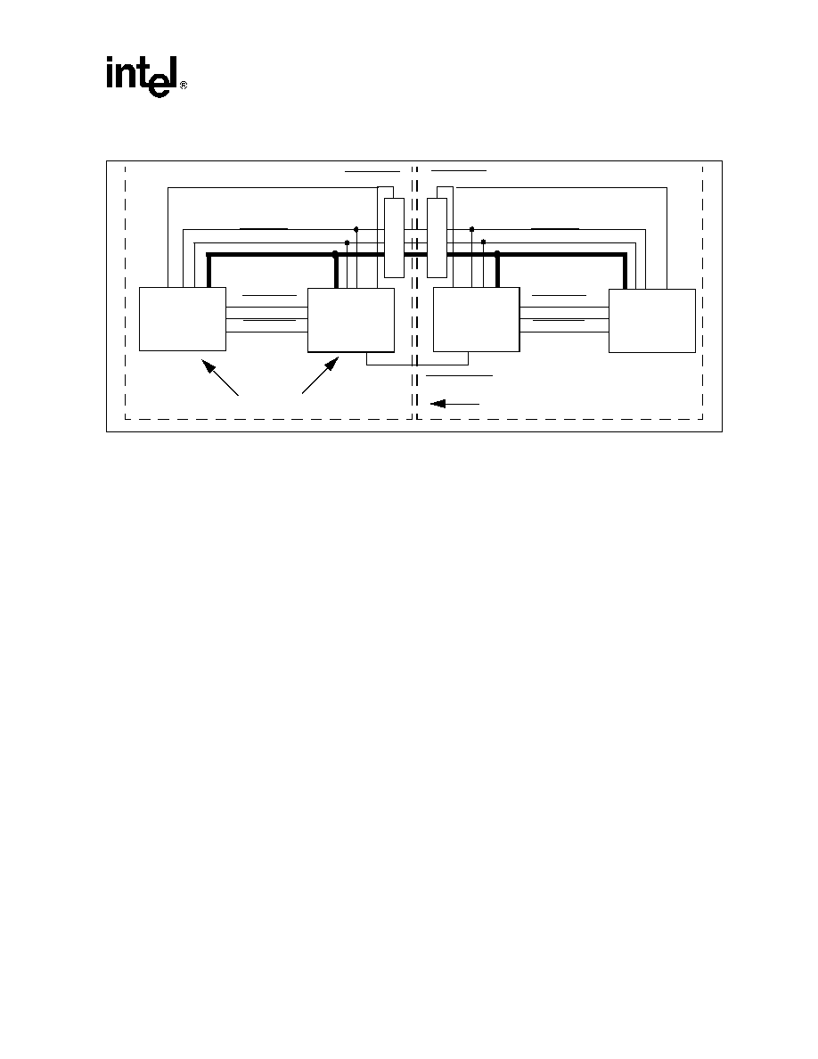
Advanced 10/100 Repeater with Integrated Management -- LXT9860/9880
Datasheet
Document #: 248987
Revision#: 003
Rev Date: 08/07/01
49
Figure 8. 100 Mbps IRB Connection
IR100DAT(4:0)
IR100DV
IR100CLK
IR100CFS
IR100DAT(4:0)
IR100DV
IR100CLK
IR100CFSBP
HUB #1
HUB #2
74L
V
T
245
74L
V
T
245
IR100DEN
IR100DEN
IR100SNGL
IR100COL
IR100CFS
IR100SNGL
IR100COL
LXT98x0
LXT98x0
(00)
LXT98x0
(00)
LXT98x0
Cascade
Stack

LXT9860/9880 -- Advanced 10/100 Repeater with Integrated Management
50
Datasheet
Document #: 248987
Revision#: 003
Rev Date: 08/07/01
Figure 9. IRB Block Diagram
Table 19. Cascading and Stacking Connections
Signal Type
Connections Between Devices
(Cascading)
Connections Between Boards
(Stacking)
Local
Connect all.
Do not connect.
Stack
For devices with ChipID
00, pull-up at each
device and do not interconnect.
Connect devices with ChipID = 00 between
boards. Use one pull-up resistor per stack.
Full
Connect all.
Connect using buffers.
Special (xxISO)
For devices with ChipID
00, leave open.
For device with ChipID
=
00, connect to
buffer enable.
Do not connect.
MMSTR OUT
MMSTR OUT
Digital IRB signals include IRnDAT, IRnCOL, IR10COLBP, IRnENA and IRnCLK.
Local Analog IRB signal: IRnCFS.
Inter-Board Analog IRB signal: IRnCFSBP.
This diagram shows a single IRB. The LXT98xx actually has two independent IRBs, one per speed/segment.
'245
9880 ChipID = 0
9880 ChipID = 1
9880 ChipID = n
Hub Board 1
Digital IRB Signals
Analog IRB Signals
MMSTR
OUT / IN
MMSTR
OUT / IN
MMSTR
OUT
MMSTR
IN
ISOLATE
IRDEN
HOLDCOL
'245
988 ChipID = 0
9880 ChipID = 1
9880 ChipID = n
Hub Board 2
Digital IRB Signals
Analog IRB Signals
MMSTR
OUT / IN
MMSTR
OUT / IN
MMSTR
OUT
MMSTR IN
ISOLATE
IRDEN
HOLDCOL
'245
9880 ChipID = 0
9880 ChipID = 1
9880 ChipID = n
Hub Board n
Digital IRB Signals
Analog IRB Signals
MMSTR
OUT / IN
MMSTR
OUT / IN
MMSTR
OUT
MMSTR IN
ISOLATE
IRDEN
HOLDCOL
MMSTR OUT / IN
HOLDCOL, MMSTRIN, and MMSTROUT are used on the 10M IRB Only.

Advanced 10/100 Repeater with Integrated Management -- LXT9860/9880
Datasheet
Document #: 248987
Revision#: 003
Rev Date: 08/07/01
51
3.9
MII Port Operation
The LXT98x0 MII ports allow direct connection with a MAC. The MII ports can operate at either
10 Mbps or 100 Mbps. Speed control is provided via MIIn_SPD. For 100 Mbps operation, set
MIIn_SPD = 1. For 10 Mbps operation, set MIIn_SPD = 0.
The LXT98x0 maintains the same statistics for the MIIs as it does for the 10/100 ports (except for
isolate, partition, and illegal symbols). The LXT98x0 does not provide MDIO/MDC capability, as
this is provided via the Serial Management Interface (SMI).
3.9.1
Preamble Handling
When operating at 100 Mbps, the LXT98x0 passes the full 56 bits of preamble through before
sending the SFD. When operating at 10 Mbps, the LXT98x0 sends data across the MII starting
with the 8-bit SFD (no preamble bits).
Note:
MII Ports do not count partition, isolation, or symbol errors.
Table 20. IRB Signal Details
Name
Pad Type
Buffer
Pull-up
Connection Type
100 Mbps IRB Signals
IR100DAT<4:0>
Digital
Yes
No
Full
IR100CLK
Digital
Yes
1K
Full
IR100DV
Digital, Open Drain
Yes
300
Full
IR100CFS Analog
No
215
, 1%
Local
IR100CFSBP Analog
No
91
, 1%
Stack
IR100COL Digital
No
No
Local
IR100SNGL Digital
No
No
Local
IR100DEN
Digital, Open Drain
N/A
1
330
Local
IR100ISO
Digital
N/A
1
No
Special
10 Mbps IRB Signals
IR10DAT
Digital, Open Drain
Yes
330
Full
IR10CLK
Digital
Yes
No
Full
IR10ENA
Digital, Open Drain
Yes
330
Full
IR10CFS Analog
No
215
, 1%
Local
IR10CFSBP Analog
No
330
, 1%
Stack
IR10COL Digital
No
330
, 1%
Local
IR10COLBP Digital
No
330
, 1%
Stack
IR10DEN
Digital, Open Drain
N/A
1
330
Local
IR10ISO
Digital
N/A
1
No
Special
1. Isolate and Driver Enable signals are provided to control an external bidirectional transceiver.

LXT9860/9880 -- Advanced 10/100 Repeater with Integrated Management
52
Datasheet
Document #: 248987
Revision#: 003
Rev Date: 08/07/01
3.10
Serial Management I/F
The high-speed Serial Management Interface (SMI) provides access to repeater MIB variables,
RMON Statistics attributes and status and control information. A network manager accesses the
interface through a simple serial communications controller such as an 8530 SCC. The SMI allows
multiple LXT98x0 devices to be managed from one common bus.
3.10.1
SMI Signals
The interface consists of a data input line (SRX), data output line (STX), and a clock (SERCLK).
The interface operates on a simple command response model, with the network manager as the
master and the LXT98x0 devices as slaves.
Figure 11
is a simplified view of typical serial
management interface architecture. Refer to
Figure 23 on page 68
for circuit details.
Note:
Refer to Application Note 64, High-Speed Serial Management Interface, for additional
information.
Figure 10. LXT9880 MII Operation
MIIn_TXD<3:0>
MIIn_TXEN
MIIn_TXER
MIIn_TXCLK
MIIn_RXCLK
MIIn_RXD<3:0>
MIIn_RXDV
MIIn_RXER
MIIn_CRS
MIIn_COL
LXT98x0
10/100
MAC
The two LXT98x0 MII ports act
as the PHY side of the MII. An
external MAC sends TX Data to
the LXT98x0 to be repeated to
the network. The LXT98x0
repeats network data to the MAC
via the RX Data lines.
Port 1
Port 2
Port 3
Port 4
Ports 1, 2
TP Ports
MII Ports
Port 6
Port 7
Port 8
Port 5
Figure 11. Typical SMI Bus Architecture
LXT918
LXT918
LXT9880
RMON &
Repeater MIB
Support
Serial
Controller
Network
Management
User
Definable
Partitioning

Advanced 10/100 Repeater with Integrated Management -- LXT9860/9880
Datasheet
Document #: 248987
Revision#: 003
Rev Date: 08/07/01
53
3.10.1.1
Serial Clock
SERCLK is a bidirectional pin; direction control is provided by the RECONFIG input. If
RECONFIG is High, the LXT98x0 drives SERCLK at 625 kHz. If RECONFIG is Low, SERCLK
is an input, between 0 and 2 MHz. The clock can be stopped after each operation, as long as an idle
(at least 12 ones in a row) is transmitted first.
3.10.1.2
Serial Data I/O
The serial data pins, SRX and STX, should be "logically" tied together using open-collector
buffers. See
Figure 23 on page 68
. The SRX input is compared with the STX output. If a mismatch
occurs, STX goes to a high impedance. STX is driven on the falling edge of SERCLK. SRX is
sampled on the rising edge.
3.10.2
Read and Write Operations
Data can be read or written in blocks. The LXT98x0 can read the full length field of consecutive
counters with a single access. Block writes are limited to 2 long words.
Normally the network manager directs read and write operations to a specific LXT98x0 device
using a two-part address consisting of HubID and Chip Address.
Note:
In the Header Field, the Chip Address is defined by three bits. The Most Significant Bit (MSB) = 0;
the value of the other two bits is set by pins.
The LXT98x0 responds to an operation within 12 serial controller bit times. In the case of an error
during a transfer, the LXT98x0 does not implement the requested command.
3.10.2.1
SMI Collision Handling
Upon colliding with another packet, the LXT98x0 ceases transmission, based on the bit pattern of
the colliding packets as shown in
Figure 12
. In the case of a collision, the driver who is sourcing a
0 wins. The LXT98x0 does not retry a response, unless it was an address arbitration packet. In
addition, if an address arbitration packet jumps in during a request/response sequence, before the
addressed LXT98x0 has responded, the addressed LXT98x0 aborts the requested operation.
Note:
The minimum time between packets must be at least 12 bit times with the data set to all ones.
3.10.2.2
SMI Address Match Indication
The LXT98x0 SER_MATCH pin (see
Figure 13
) indicates detection of a serial command matching
the device Hub ID. Broadcast commands also trigger the SER_MATCH output. Note that the initial
HubID upon power-up or reset is the Broadcast (all ones) address.

LXT9860/9880 -- Advanced 10/100 Repeater with Integrated Management
54
Datasheet
Document #: 248987
Revision#: 003
Rev Date: 08/07/01
3.10.2.3
SMI Frame Format
The SMI uses a simple frame format, shown in
Figure 14
.
Table 21
describes the individual fields.
Table 22
shows how the bits for the header field are stored in memory, assuming that they are
transmitted LSB to MSB, low address to high address.
Table 23
lists the command set and
Table 24
provides a variety of typical packets.
All frames begin and end with a simple flag consisting of "01111110". Multiple flags cause the
LXT98x0 to ignore the packet. All fields are transmitted LSB first. Zero-bit stuffing is required if
more than five 1s in a row appear in the header, data or CRC fields. In addition, all operations
directed to the device must be followed by an idle (at least 12 ones in a row), and the first operation
must be preceded with an idle.
Note:
The LXT98x0 uses the CCITT method of CRC (X
16
+ X
12
+ X
5
+1).
Figure 12. SMI Collision Handling
Figure 13. SMI Address Match Indication
Pkt 1-Succeeds
Pkt 2-Ceases, due to collision
Pkt 3-Ceases, due to collision
Data
Data
Data
Clk
1. Simultaneous Transmissions, Pkt 1 completes
Transmit om falling CLK edge, sample on rising CLK edge.
HUB ID
CHIP ID, etc.
SRX/STX
SER_MATCH
SERCLK
1. SER_MATCH can also occur at the end of a packet if a Start Flag is not seen but a Stop Flag is.
This can occur only during unit installation or removal.

Advanced 10/100 Repeater with Integrated Management -- LXT9860/9880
Datasheet
Document #: 248987
Revision#: 003
Rev Date: 08/07/01
55
Table 21. SMI Message Fields
Message
Description
Start or Stop Flag
"01111110". Protocol requires zero insertion after any five consecutive "1"s in the data
stream.
Hub ID
Identifies board or sub-system. Assigned by one of two arbitration mechanisms at power-
up.
Chip ID
Identifies one of eight devices on a system. Assigned by 2 external pins on each device.
The Most Significant Bit (MSB) = 0; the value of the other two bits is set by pins.
Command
Identifies the particular operation being performed (see
Table 23
)
Length
Specifies number of registers to be transferred (1 to 127). Maximum is 2 per write, 127 per
read.
Address
Specifies address of register or register block to be transferred.
Figure 14. Serial Management Frame Format
Table 22. SMI Header Storage
MSB
LSB
Increasing
Address
Addr 11
Addr 10
Addr 9
Addr 8
Addr 7
Addr 6
Addr 5
Addr 4
Addr 3
Addr 2
Addr 1
Addr 0
Length 6
Length 5
Length 4
Length 3
Length 2
Length 1
Length 0
CMD 4
Cmd 3
Cmd 2
Cmd 1
Cmd 0
Chip
Address
Bit 2
(set to 0)
Chip
Address
Bit 1
Chip
Address
Bit 0
HubID 4
HubID 3
HubID 2
HubID 1
HubID 0
Hub ID
Chip Add
Cmd
Length
7 bits
Address
12 bits
Data
(0-508 bytes)
Start
Flag
Header
CRC
(2 bytes)
Stop
Flag
Idle
Idle
Header Content:
5 bits
3 bits
5 bits

LXT9860/9880 -- Advanced 10/100 Repeater with Integrated Management
56
Datasheet
Document #: 248987
Revision#: 003
Rev Date: 08/07/01
Table 23. SMI Command Set
Command
Value
Name
Usage
Normally
Sent By
Description
18 (Hex)
Write
Normal Ops
Network Mgr
Used to set a register or group of registers. The
minimum write size is 1 long word. The maximum
block write is 2 long words. This size was chosen
so that software may write an entire Ethernet
address in one serial packet.
04 (Hex)
Read
Normal Ops
Network Mgr
Used to get complete sets of counter information
for either a port or a segment. The minimum read
size is 32 bits (one long word). The maximum block
read is 127 long words. The acknowledge for this
instruction is the actual returned data.
08 (Hex)
Request ID
Arbitration
LXT98x0
For Hub ID (Arb Method 1): The LXT98x0 repeats
this command periodically until it is assigned a Hub
ID. Once assigned, the command is discontinued.
00 (Hex)
ConfigChg
Arbitration
LXT98x0
Notifies system of configuration change (hot swap).
Requests new arbitration phase.
10 (Hex)
Re-arbitrate
Arbitration
Network Mgr
Re-starts arbitration. Assigns all new addresses.
14 (Hex)
Assign
HubID
Chain
Arbitration
Network Mgr
Assigns Hub ID to device with ARBIN = 0 and
ARBOUT = 1
0C (Hex)
Set Arbout
to 1
Chain
Arbitration
Network Mgr
Used to determine stacking order or assign
address. Commands specific device to set
ARBOUT= 1. This command can apply to either a
single LXT98x0 (via direct addressing), or every
LXT98x0 through the use of the broadcast
address.
1C (Hex)
Set Arbout
to 0
Chain
Arbitration
Network Mgr
Used to determine stacking order or assign
address. Commands specific device to set
ARBOUT = 0. This command can apply to either a
single LXT98x0 (via direct addressing), or every
LXT98x0 through the use of the broadcast
address.
02 (Hex)
DevID
Config
Network Mgr
Asks device to send contents of device revision
register. This command applies to only a single
LXT98x0 at a time. When given, the command
causes the chip to retrieve its type and revision
code data (hard coded for a given device) and
provide it to the serial controller for transmission
back to the requesting manager. The acknowledge
for this type of packet is the actual returned data.
This command can also be used for `ping'
operations.

Advanced 10/100 Repeater with Integrated Management -- LXT9860/9880
Datasheet
Document #: 248987
Revision#: 003
Rev Date: 08/07/01
57
3.10.3
Address Assignment Methods
Each device has a two part address, consisting of a HubID and a Chip Address (See
Figure 14 on
page 55
). The Chip Address is assigned by the input pins CHIPID<1:0>. (The Most Significant Bit
[MSB] = 0.)
The manager assigns the HubID. Each LXT98x0 on a particular board has the same HubID. The
HubID is assigned through one of two arbitration mechanisms as shown in
Figure 15
.
Table 24. Typical Serial Management Packets
Message
Contents of Fields in Serial Management Packet
Hub ID
Chip
Address
5
Command
Length
Address
Data
Write
1, 2
User defined
User defined
18 Hex
01 or 02 Hex
User defined
User defined
Read Request
1, 3, 4
User defined
User defined
04 Hex
01 to 7F Hex
User defined
Null
Read Response
3
00000
000
04 Hex
01 to 7F Hex
User defined
Data values
Assign Hub ID
(Arb Method 1)
11111
011
18 Hex
02 Hex
188 Hex
Formatted per
Table 89 on
page 115
and
Table 90 on
page 116
Assign Hub ID
(Arb Method 2)
11111
011
14 Hex
01 Hex
000 Hex
Hub ID (LSB)
and 27 0s
Set Arbout to 0
User defined
User defined
1C Hex
00 Hex
000 Hex
Null
Set Arbout to 1
User defined
User defined
0C Hex
00 Hex
000 Hex
Null
Arb Request
00000
000
08 Hex
02 Hex
190 Hex
PROM ID
Resend Arbitration
11111
011
10 Hex
00 Hex
000 Hex
Null
Resend Arbitration
Response
00000
000
08 Hex
02 Hex
190 Hex
PROM ID
Device type/
Revision code
User defined
User defined
02 Hex
01 Hex
000 Hex
Null
Device/Revision
Response
00000
000
02 Hex
01 Hex
13C Hex
Device type/
revision
1. Other than checking that the top 3 bits of the address equals 000, the LXT98x0 does not check if the user
writes or reads past the highest location. There are no adverse effects for writing or reading locations
above the specified range.
2. If the user performs a write operation of length 1 or 2 and does not send a data field, the LXT98x0 writes
junk into the specified registers. This constitutes an invalid command.
3. If the user reads past the highest location of the LXT98x0, all those locations reads back 0s.
4. If a read operation is performed with a length of 0, the LXT98x0 does not respond.
5. ChipID is defined by 3 bits, with the MSB = 0; value of the other two bits is set by pins.

LXT9860/9880 -- Advanced 10/100 Repeater with Integrated Management
58
Datasheet
Document #: 248987
Revision#: 003
Rev Date: 08/07/01
3.10.3.1
Chain Arbitration Mechanism
The chain method is the easiest and requires no serial PROM. The ARBSELECT pin on all devices
must be set to 1. When constructing the stack, the designer creates a daisy chain by tying the
ARBOUT pin of each LXT98x0 to the ARBIN pin of the following LXT98x0. The manager is at
the top of the stack and controls the ARBIN for the first LXT98x0. The manager progressively
assigns Hub IDs using the Assign Hub ID (Arb Method 2) and Set ARBOUT to ZERO commands.
The manager initially sets its ARBOUT (first LXT98x0's ARBIN) to zero. Since the Assign Hub
ID (Arb Method 2) command only works on the LXT98x0 with ARBIN of 0 and an ARBOUT of
1, the first LXT98x0 can be assigned an address. After the first LXT98x0 has been assigned an
address, it can uniquely be told to switch its ARBOUT to zero. This creates the (01) condition on
the next LXT98x0 in the line. This LXT98x0 is then assigned an address and the process continues
until all chips have been assigned a unique address.
Note:
It is recommended that HubIDs match in any given hub.
The manager can verify that a hub is still present by performing DEVICE ID commands. If a
change of configuration is detected, the manager can perform a broadcast write to return each hub's
ARBOUT to 1, and then re-perform the address assignment process.
When using the chain arbitration method, set up the daisy chain so the device with ChipID = 00 is
the first device in the board that the chain passes through. When assigning IDs, the `1st in Chain'
bit in the device revision register (refer to
Table 77 on page 111
) can be used to determine when a
new board has been encountered.
3.10.3.2
PROM Arbitration Mechanism
This mechanism requires one serial PROM with a unique 48-bit ID in each board. This ID can
consist of serial number, date/week/year of manufacture, etc. The ARBSELECT pin must be set to
0. At power-up, the device with ChipID = 00 reads a 48-bit ID from the PROM. All other devices
Figure 15. Address Arbitration Mechanisms
1
LXT98x0
ARBIN
ARBOUT
Network
Manager
ARBOUT
Serial I/F to Next Module
SRX/STX
LXT98x0
ARBIN
ARBOUT
SRX/STX
0
SRX/STX
Hub Board 1
1
LXT98x0
ARBIN
ARBOUT
SRX/STX
1
LXT98x0
ARBIN
ARBOUT
SRX/STX
0
Hub Board 2
ARBI/O Chain to Next Module
0
Chain Mechanism for
Address Arbitration
Network
Manager
Serial I/F to Next Module
SRX/STX
Hub Board 1
Serial
EPROM
LXT98x0
SRX/STX
PROMDTI/O
LXT98x0
SRX/STX
PROMDTI/O
Hub Board 2
Serial
EPROM
LXT980
SRX/STX
PROMDTI/O
LXT980
SRX/STX
PROMDTI/O
EPROM Mechanism
for Address Arbitration

Advanced 10/100 Repeater with Integrated Management -- LXT9860/9880
Datasheet
Document #: 248987
Revision#: 003
Rev Date: 08/07/01
59
on the board listen in and record the ID. The device with ChipID = 00 then transmits Arbitration
Request messages on the SMI every 2-3 ms. The request messages from two boards may collide. If
this happens, a resolution scheme ensures that only one message is transmitted.
The network manager must respond to each request with a message that includes the 48-bit ID and
the HubID. All devices hear this message, but only those matching the 48-bit ID receive the HubID
as their own. Once a HubID is assigned to a hub, that hub ceases requesting a HubID. This process
continues until all hubs are assigned an ID. Should a hub power off and back on, the hub re-
requests an ID, which the manager provides. An address arbitration packet is selected over normal
requests.
3.10.3.3
Address Re-Arbitration
There are two mechanisms for address re-arbitration following a configuration change, such as a
hot-swap of a board:
∑
Manual Re-arbitration. If the LXT98x0 detects a Low-to-High transition on RECONFIG, or if
RECONFIG is High at power-up, it sends out a "Configuration Change" message (Start Flag
with all 0s) on the bus. The network manager can use this message to detect that re-arbitration
is required.
∑
Network Manager. The network manager can detect or re-start arbitration at any time by
sending the "Re-arbitrate" command.
3.10.4
Interrupt Functions
The LXT98x0 provides a single open-collector pin for external interrupt signalling. Several
different interrupt conditions may be reported. The Interrupt Status Register (see
Table 86
)
identifies the specific interrupt condition. The Interrupt Mask Register (see
Table 87 on page 115
)
allows specific interrupts to be masked. Interrupts may be cleared in two ways, depending on the
status of bit 11 in the repeater configuration register.
3.11
Serial PROM Interface
The serial PROM interface allows the vendor to load in optional information unique to each board.
Items such as serial number or manufacture date can be placed in the serial PROM which can also
be used in the address arbitration process. Each board must contain a unique set of information.
Additionally, only 1 serial PROM is required per board, they are not required per chip. The
LXT98x0 reads in the first 48 bits (three 16-bit words) from the PROM and stores them in a
register. This read occurs only on power-up. Only the LXT98x0 with a ChipID of 00 drives the
serial PROM control lines; all other LXT98x0s "listen" to the data and clock lines. The first bit into
the LXT98x0 from this interface corresponds to bit 47. The serial PROM shifts out the most
significant bit (15) of the word first (the PROM must be auto-incrementing).

LXT9860/9880 -- Advanced 10/100 Repeater with Integrated Management
60
Datasheet
Document #: 248987
Revision#: 003
Rev Date: 08/07/01
3.12
Serial Configuration Interface
The Serial Configuration Interface allows the user to load system-specific information (board type,
plug-in cards, status, etc.) into the Repeater Configuration Register (see
Table 75 on page 109
).
This register may be read remotely through the Serial Management Interface (SMI). The Serial
Configuration Interface mode (Repeater Configuration Register bit 14 = 1) allows the collection of
up to 8 bits of board data, compared to the CONFIG[1:0] 2-bit mode (bit 14 = 0). See
Table 75 on
page 109
.
For Serial Configuration Interface mode = 1, an external `165 device is used to perform a parallel-
to-serial conversion of the board data (see
Figure 17
). These board data bits are shifted into the
LXT98x0 each time the Repeater Serial Configuration register is read. CFG_DT is clocked into the
LXT98x0 relative to the rising edge of CFG_CLK as shown in
Figure 18
. Also note the register bit
positions versus the `165 parallel input positions.
The CFG_CLK pin is shared with LED_CLK. For reading the Repeater Serial Configuration
Register, the configuration bits are reloaded into the LXT98x0. The shared functionality of the
clock (configuration and serial LED), causes an unscheduled serial LED update. All 32 clock
cycles occur with only the first 8 bits clocked into the Repeater Serial Configuration Register. See
Table 76 on page 110
.
Figure 16. Optional R/W Serial PROM Interface
CLK
DTOUT
The LXT98x0 drives outgoing data on the falling clock edge.
The LXT98x0 samples incoming data on the rising clock edge
.
CS

Advanced 10/100 Repeater with Integrated Management -- LXT9860/9880
Datasheet
Document #: 248987
Revision#: 003
Rev Date: 08/07/01
61
4.0
Application Information
4.1
General Design Guidelines
Following generally accepted design practices is essential to minimize noise levels on power and
ground planes. Up to 50 mV of noise is considered acceptable. 50 to 80 mV of noise is considered
marginal. High-frequency switching noise can be reduced, and its effects can be eliminated, by
following these simple guidelines throughout the design:
∑
Fill in unused areas of the signal planes with solid copper. Attach them with vias to a VCC or
ground plane that is not located adjacent to the signal layer.
∑
Use ample bulk and decoupling capacitors throughout the design (a .01
µ
F value is
recommended for decoupling caps).
∑
Provide ample power and ground planes.
∑
Provide termination on all high-speed switching signals and clock lines.
∑
Provide impedance matching on long traces to prevent reflections.
∑
Route high-speed signals next to a continuous, unbroken ground plane.
∑
Filter and shield DC-DC converters, oscillators, etc.
Figure 17. Serial Configuration Interface
Figure 18. Serial Configuration Interface Signaling
`165
CFG_CLK
CFG_DT
LXT98x0
CFG_
LD
CLK
Q
H
SH/
LD
A B C D E F G H
Parallel Config. Data
SER
CFG_
LD
CFG_DT
G = b1
F = b2
E= b3
D = b4
C = b5
B = b6
A = b7
CFG_CLK
100 ns / 10 MHz
H = b0

LXT9860/9880 -- Advanced 10/100 Repeater with Integrated Management
62
Datasheet
Document #: 248987
Revision#: 003
Rev Date: 08/07/01
∑
Do not route any digital signals between the LXT98x0 and the RJ-45 connectors at the edge of
the board.
∑
Do not extend any circuit power and ground plane past the center of the magnetics or to the
edge of the board. Use this area for chassis ground, or leave it void.
4.2
Typical Applications
Figure 19
and
Figure 20
are simplified block diagrams showing typical applications.
Figure 21
through
Figure 26
show application circuitry details.
Figure 19. 8-Port Managed 10/100 Stackable Repeater
Figure 20. 32-Port Managed 10/100 Repeater
Serial Comm Controller
Bridge
10M
MAC
100M
MAC
74LVT245
8 10/100 Ports
Serial
Port
10M
IRB
100M
IRB
TP
Ports
MII
2
MII
1
74LVT245
Serial Comm Controller
Bridge
10M
MAC
100M
MAC
74LVT245
32 10/100 Ports
Serial
Port
10M
IRB
100M
IRB
TP
Ports
MII
2
MII
1
Serial
Port
10M
IRB
100M
IRB
TP
Ports
MII
2
MII
1
Serial
Port
10M
IRB
100M
IRB
TP
Ports
MII
2
MII
1
Serial
Port
10M
IRB
100M
IRB
TP
Ports
MII
2
MII
1
RMON
(Optional
10M or 100M
MAC
74LVT245

Advanced 10/100 Repeater with Integrated Management -- LXT9860/9880
Datasheet
Document #: 248987
Revision#: 003
Rev Date: 08/07/01
63
4.3
Application Circuitry
4.3.1
Power and Ground
4.3.1.1
Supply Filtering
Power supply ripple and digital switching noise on the VCC plane causes EMI and degrades line
performance. Predicting a design's performance is difficult, although certain factors greatly
increase the risks:
∑
Poorly-regulated or over-burdened power supplies.
∑
Wide data busses (>32-bits) running at a high clock rate.
∑
DC-to-DC converters.
Many of these issues can be improved by following good general design guidelines. In addition,
Intel recommends filtering between the power supply and the analog VCC pins of the LXT98x0.
Filtering has two benefits. First, it keeps digital switching noise out of the analog circuitry inside
the LXT98x0, which helps line performance. Second, if the VCC planes are laid out correctly, it
keeps digital switching noise away from external connectors, reducing EMI.
The VCC plane should be divided into two sections. The digital section supplies power to the
digital VCC pins and to the external components. The analog section supplies power to VCCR and
VCCT pins of the LXT98x0. The break between the two planes should run under the device. In
designs with more than one LXT98x0, use a single continuous analog VCC plane to supply them
all.
The digital and analog VCC planes should be joined at one or more points by ferrite beads. The
beads should produce at least a 100
impedance at 100 MHz. The beads should be placed so
current flows evenly. The maximum current rating of the beads should be at least 150% of the
current that is actually expected to flow through them. Each LXT98x0 draws a maximum of
1000mA from the analog supply so beads rated at 1500mA maximum should be used. A bulk cap
(2.2 -10
µ
F) should be placed on each side of each ferrite bead to ground to stop switching noise
from traveling through the ferrite.
In addition, a high-frequency bypass cap (.01
µ
f) should be placed near each analog VCC pin to
ground.
4.3.1.2
Ground Noise
The best approach to minimize ground noise is strict use of good general design guidelines and by
filtering the VCC plane.
4.3.1.3
Power and Ground Plane Layout Considerations
The power and ground planes should be laid out carefully. The following guidelines are
recommended:
∑
Follow the guidelines in the Application Note 113 (LXT98x0 Design and Layout Guide) for
locating the split between the digital and analog VCC planes.
∑
Keep the digital VCC plane away from the TPOP/N and TPIP/N signals, magnetics, and RJ-45
connectors.

LXT9860/9880 -- Advanced 10/100 Repeater with Integrated Management
64
Datasheet
Document #: 248987
Revision#: 003
Rev Date: 08/07/01
∑
Place the layers so the TPOP/N and TPIP/N signals are routed near or next to the ground
plane. For EMI, it is more important to shield TPOP/N than TPIP/N.
4.3.1.4
Chassis Ground
For ESD protection, create a separate chassis ground. For isolation, encircle the board and place a
"moat" around the signal ground plane to separate signal ground from chassis ground. Chassis
ground should extend from the RJ-45 connectors to the magnetics, and can be used to terminate
unused signal pairs (`Bob Smith' termination). In single-point grounding applications, provide a
single connection between chassis and circuit grounds with a 2kV isolation capacitor. In multi-
point grounding schemes (chassis and circuit grounds joined at multiple points), provide 2kV
isolation to the Bob Smith termination.
4.3.1.5
The RBIAS Pin
The LXT98x0 requires a 22.1 k
,
1% resistor directly connected between the RBIAS pin and
ground. Place the RBIAS resistor as close to the RBIAS pin as possible. Run an etch directly from
the pin to the resistor, sink the other side of the resistor, and surround the RBIAS trace with a
filtered ground. Do not run high-speed signals next to RBIAS.

Advanced 10/100 Repeater with Integrated Management -- LXT9860/9880
Datasheet
Document #: 248987
Revision#: 003
Rev Date: 08/07/01
65
4.3.2
MII Terminations
The LXT98x0 MIIs have high output impedance (250-350
). To minimize reflections, serial
termination resistors are recommended on all MII signals, especially with designs with long traces
(>3 inches). Place the resistor as close to the device as possible. Use a software trace termination
package to select an optimal resistance value for the specific trace. Proper value = nominal trace
impedance minus 13
. If a software package cannot be used and nominal trace impedance is not
known, use 55
.
4.3.3
Twisted-Pair Interface
The LXT98x0 transmitter uses standard 1:1 magnetics for both receive and transmit. Nonetheless,
system designers should take precautions to minimize parasitic shunt capacitance and meet return
loss specifications. These steps include:
Figure 21. Power and Ground Connections
RBIAS
VCC
GND
GND
VCCR
GND
.01
µ
F
22.1 k
1%
GND
VCC
0.1
µ
F
+
Ferrite
Beads
10
µ
F
+3.3V
LXT9880
VCCT
GND
10
µ
F
.01
µ
F
.1
µ
F
.1
µ
F
Digital Supply Plane
Analog Supply Plane
.01
µ
F
.1
µ
F
To Output Magnetics Centertap

LXT9860/9880 -- Advanced 10/100 Repeater with Integrated Management
66
Datasheet
Document #: 248987
Revision#: 003
Rev Date: 08/07/01
∑
Place magnetics as close as possible to the LXT98x0.
∑
Keep transmit pair traces short.
∑
Do not route transmit pair adjacent to a ground plane. Eliminate planes under the transmit
traces completely. Otherwise, keep planes 3-4 layers away.
∑
Improve EMI performance by filtering the output center tap supply. A single ferrite bead may
be used in the center tap supply to all ports. A ferrite bead with a total maximum current rating
of 1.5Amp is recommended.
∑
Place 270pF 5% capacitors at TPIP and TPIN to improve signal-to-noise immunity at the
receiver, especially for long line lengths.
In addition, follow all the standard guidelines for a twisted-pair interface:
∑
Route the signal pairs differentially, close together. Allow nothing to come between them.
∑
Keep distances as short as possible; both traces should have the same length.
∑
Avoid vias and layer changes.
∑
Keep the transmit and receive pairs apart to avoid cross-talk.
∑
To provide maximum isolation, place entire receive termination network on one side and
transmit on the other side of the PCB.
∑
Bypass common-mode noise to ground on the in-board side of the magnetics using 0.01
µ
F
capacitors.
∑
Keep termination circuits grouped closely together and on the same side of the board.
∑
Always put termination circuits close to the source end of any circuit.
4.3.3.1
Magnetics Information
The LXT98x0 requires a 1:1 ratio for the receive transformers and a 1:1 ratio for the transmit
transformers. The transformer isolation voltage should be rated at 2 kV to protect the circuitry from
static voltages across the connectors and cables. Refer to
Table 25
for magnetics specifications.
4.3.4
Clock
A stable, external 25 MHz system clock source (CMOS) is required. See
Table 26
.
Table 25. LXT98x0 Magnetics Specifications
Parameter
Min
Nom
Max
Units
Test Condition
Rx turns ratio
≠
1 : 1
≠
≠
Tx turns ratio
≠
1 : 1
≠
≠
Insertion loss
0.0
≠
1.1
dB
80 MHz
Primary inductance
350
≠
≠
µ
H
Transformer isolation
≠
2
≠
kV
Differential to common mode rejection
-40
≠
dB
.1 to 60 MHz
-35
≠
dB
60 to 100 MHz
Return Loss - standard
-16
≠
dB
30 MHz
-10
≠
dB
80 MHz

Advanced 10/100 Repeater with Integrated Management -- LXT9860/9880
Datasheet
Document #: 248987
Revision#: 003
Rev Date: 08/07/01
67
Table 26. Oscillator Manufacturers
Manufacturer
Part Number
Frequency
CTS
MXO45 / 45LV
25 MHz
Epson America
SG-636 Series
25 MHz
Figure 22. Typical Twisted-Pair Port Interface and Power Supply Filtering
TPFIP
TPIN
RJ45
TPOP
TPON
VCCT
GND
0.1
µ
F
.01
µ
F
50
1%
T
o
T
w
i
s
te
d
-
Pa
i
r
N
e
tw
o
r
k
3
6
1
2
1:1
1:1
LXT98x3
50
50
50
50
50
50
4
5
8
7
50
1%
0.01
µ
F
5%
270 pF 5%
270 pF 5%
0.001
µ
F
2kV
0.001
µ
F
2kV
0.001
µ
F
2kV
TPIP
.01
µ
F

LXT9860/9880 -- Advanced 10/100 Repeater with Integrated Management
68
Datasheet
Document #: 248987
Revision#: 003
Rev Date: 08/07/01
4.3.5
SMI and PROM Circuits
Figure 23. Typical Serial Management Interface Connections
Figure 24. Serial Controller Connection Showing PAL
VCC
74xx05
SRX
STX
1. When not transmitting STX goes to 1, hence
open collector and no drive.
8530
RxDA
TxDA
RTxCA
CTSA
OC
Driver
CLK
Serial
Line
PAL
RTSA
1. PAL is used to detect collisions and gate (cease) transmission.
The PAL notifies the 8530 to abort the current transmission via
the CTS bit, which is then cleared by the RTS bit.

Advanced 10/100 Repeater with Integrated Management -- LXT9860/9880
Datasheet
Document #: 248987
Revision#: 003
Rev Date: 08/07/01
69
4.3.6
LED Circuits
4.3.6.1
Direct Drive LEDs
Each Direct Drive LED has a corresponding open-drain pin. The LEDs are connected, via a current
limiting resistor, to a positive voltage rail. The LEDs are turned on when the output pin drives Low.
The open-drain LED pins are 5V tolerant, allowing use of either a 3.3V or 5V rail. A 5V rail eases
LED component selection by allowing more common, high forward voltage LEDs to be used.
Refer to
Figure 27
for a circuit illustration.
4.3.6.2
LED Pins Multiplexed with Configuration Inputs
Some static configuration inputs are multiplexed with LED pins to reduce the LXT98x0 pin count.
These LED pins are configured by current sinking (open- drain output) and sourcing (open-source
output). If the LED pin sinks the LED current, the configuration value is `1'. If LED pin sources
Figure 25. Serial PROM Interface
Figure 26. Typical Reset Circuit
93CS46
PROM_CS
PROM_CLK
PROM_DTIN
PROM_DTOUT
PROM_DTIN
PROM_CLK
LXT98x0
(ID = 00)
LXT98x0
(ID
00
)
VCC
C
R1
R2
'14
D
1. t(CR1 > Power Supply Ramp Up Time. R2 discharges C when supply
goes away. The `14 is needed for multiple LXT98x0 devices.

LXT9860/9880 -- Advanced 10/100 Repeater with Integrated Management
70
Datasheet
Document #: 248987
Revision#: 003
Rev Date: 08/07/01
the current, the configuration value is a `0'. The LXT98x0 detects the configuration value
following reset and then selects the appropriate output drive circuit (open drain or source). If the
LED function of a multiplexed configuration pin is not used, tie the pin to Ground or Vcc via a
100≠500 k
resistor to set the configuration value. Multiple LED configuration pins can be tied off
with a single resistor to set them all to the same value. Refer to
Figure 27
for a circuit illustration.
For configuration values of `1', a 3.3V or a 5V rail can be used to drive the LEDs (to ease LED
selection as with Direct Drive LEDs).
For configuration values of `0', external buffering is used when 5V LED driving is desired. (This
buffering could be as simple as a single transistor.) As an alternative, use the copies of the
multiplexed LED data found on the LED serial interface. If a 5V tolerant serial-to-parallel device is
used for the LED serial interface, 5V LED driving is achieved (see
"Serial LEDs" on page 70
).
4.3.6.3
Serial LEDs
The LXT98x0 provides a serial interface to support additional LED options. Standard shift
registers, either 74X595s (8-bit Serial-to-Parallel with Output Registers) or 74X164s (8-bit S/P
without registers) can be used to drive these additional LEDs. Collision10/100 and Activity10/100
status indications are provided on multiplexed configuration pins and duplicated on the serial port.
The LED serial interface consists of three outputs: clock (LEDCLK), parallel latch clock
(LEDLAT), and output data (LEDDAT). The parallel latch clock is used only with the 74X595
implementation. Refer to
Figure 28
for an illustration of the LED serial interface circuit.
Potentially, 30 LEDs can be driven by the LED serial interface via 4 S/P devices. The S/P serial
output is connected to the serial input of the first serial input device. To expand the chain, connect
the last serial output to serial input of next serial interface device.
Serial LED data is output in the anticipated priority order, from least likely to most likely to be
used:
∑
Unused `595/`164 parallel outputs
∑
MII Ports - LED1, 2, 3
Figure 27. LED Circuits - Direct Drive & Multiplexed Configuration Inputs
Inside
IC
Outside
IC
Direct Drive
R
V
LED
Inside
IC
Outside
IC
Configuration
= `1'
Inside
IC
Outside
IC
Configuration
= `0'
R
V
LED
R
V
LED
= 3.3 to 5 Volts +/- 5%
Multiplexed
Multiplexed
V
cc
= 3.3 Volts +/- 5%
Inside
IC
Outside
IC
Configuration
= `0'
V
cc
Multiplexed
with Transistor Buffer
R
V
LED
100k
Rb
V
cc

Advanced 10/100 Repeater with Integrated Management -- LXT9860/9880
Datasheet
Document #: 248987
Revision#: 003
Rev Date: 08/07/01
71
∑
Miscellaneous LEDs (Repeat of Collision10/100, Manager Present, Repeat of Activity10/100,
Global Fault, RPS Fault)
∑
ACTGLED10
∑
ACTGLED100
This allows the user to leave off devices in the serial-to-parallel chain if the LEDs associated with
that condition aren't desired. Refer to
Figure 7 on page 41
which illustrates the LED serial interface
port signalling and
Table 12 on page 41
which documents the Serial LED Stream.
If the 8 bit serial bus Configuration Mode is selected (See
"Serial Configuration Interface" on
page 60
.), unscheduled (less than 122
µ
s apart) LED Serial Port cycles occur each time the
Repeater
Serial Configuration register is read. If the 74x164 buffer is used, flicker is minimized by
design so that it is not noticeable to the eye. The LED outputs may change momentarily.
4.4
Inter-Repeater Backplane Compatibility
The Inter-repeater Backplane (IRB) comprises two parts:
∑
Local--the backplane between cascaded devices on the same board.
∑
Stack--the backplane between multiple boards.
Each of these backplanes consists of both analog and digital signals.
Figure 28. Serial LED Circuit
SER
RCLK
SRCLK
Qa
Qb
.
.
.
Qh
Qh`
LED cct.
LED cct.
LED cct.
R
V
LED
LED cct.
V
LED
side
.
.
.
V
LED
= 3.3 to 5 Volts +/- 5%
74X595
.
.
.
LED cct.
LED cct.
LED cct.
.
.
.
Up to 2 more
`595s/8xLEDs
LEDDAT
LEDLAT
LEDCLK
.
.
.
Up to 2 more
`164s/8xLEDs
LED cct.
LED cct.
LED cct.
V
LED
.
.
.
LED cct.
LED cct.
LED cct.
.
.
.
LEDDAT
LEDCLK
Qa
Qb
.
.
.
Qh
A
B
CLK
74X164
Qa
Qb
.
.
.
Qh
A
B
CLK
74X164
A
C
TG
LE
D
1
00
AC
TG
L
E
D1
0
A
C
TG
LE
D
1
00
AC
TG
L
E
D1
0
SER
RCLK
SRCLK
Qa
Qb
.
.
.
Qh
Qh`
74X595
LXT98x0
LXT98x0

LXT9860/9880 -- Advanced 10/100 Repeater with Integrated Management
72
Datasheet
Document #: 248987
Revision#: 003
Rev Date: 08/07/01
4.4.1
Local Backplane--3.3V Only
The LXT98x0 local backplane operates at 3.3V only. LXT98x and LXT91x devices operate at 5V.
LXT98x0 devices are, therefore, not cascadable with LXT98x and LXT91x devices.
Note:
Do not mix LXT98x0 with either LXT98x or LXT91x devices on the local backplanes.
4.4.2
Stack Backplane--3.3V or 5V
The LXT98x0 stack backplanes can be configured to be either 3.3V or 5V. COMP_SEL (Pin 39), a
special input pin, selects between the two voltage modes, depending on whether 3.3V or 5V is
applied.
3.3V-Only Stacks
Apply 3.3V to COMP_SEL, IR100CFSBP, IR10CFSBP, and
IR10COLBP for LXT98x0 backplane operation
For 5V Backwards
Stackability
Apply 5V to COMP_SEL, IR100CFSBP, IR10CFSBP, and IR10COLBP
for LXT98x and LXT91x backplane operation.
With either mode (3.3V or 5V), COMP_SEL draws less than 3 mA.
Note:
1. The external pull-up resistor values remain the same, regardless of 3.3V or 5V backplane
operation.
2. The recommended digital signal external buffer has been changed to 74LVT245 for the
LXT98x0.
4.4.2.1
3.3V and 5.0V Stacking Boards Cannot Be Mixed
3.3V Operation
Boards designed for 3.3V backplane operation should only be stacked with other 3.3V boards.
Existing LXT98x or LXT91x based designs cannot operate in 3.3V.
Incompatible Stacking
Configurations
The following stacking configurations are incompatible:
∑
A LXT98x0-based board configured for 3.3V backplane operation and LXT98x or LXT91x
based boards (5V only).
∑
A LXT98x0-based board configured for 3.3V backplane operation and a LXT98x0-based
board configured for 5V backplane operation.
Note:
Stacking boards designed for 3.3V backplane operation with boards designed for 5V backplane
operation causes network errors.
5V Operation
Boards designed for 5V backplane operation should only be stacked with other 5V boards:
∑
LXT98x or LXT91x-based designs.
∑
LXT98x0 designs configured for 5V backplane operation.

Advanced 10/100 Repeater with Integrated Management -- LXT9860/9880
Datasheet
Document #: 248987
Revision#: 003
Rev Date: 08/07/01
73
The configuration input must be connected to 5V for compatibility with LXT98x or LXT91x-based
designs. The 5V can be supplied from the stacking cable, or a 5V source must exist within the
board itself.
Note:
Stacking boards designed for 5V backplane operation with boards designed for 3.3V backplane
operation causes network errors.
Figure 29. 100 Mbps Backplane Connection between LXT98x and LXT98x0
IR100DAT(4:0)
IR100DV
IR100CLK
IR100CFS
IR100DAT(4:0)
IR100DV
IR100CLK
IR100CFSBP
HUB #1
HUB #2
98x0
B
u
ffe
r
B
u
ffe
r
IR100DEN
IR100DEN
IR100SNGL
IR100COL
IR100CFS
IR100SNGL
IR100COL
(000)
(00)
98x0
98x
1. The LXT98x and LXT98x0 devices can share the same Inter-Repeater Backplane so long as the proper backplane
buffers are used. Configuration is set to 5V.
2. For LXT98x, LXT91x: The buffer should be the 74ABT245.
For LXT98x0: In the 5V tolerant backplane, the buffer can be either 74ABT245 or 74LVT245
3. Layout follows the same pattern for 10 Mbps operation.
98x
5V
5V

LXT9860/9880 -- Advanced 10/100 Repeater with Integrated Management
74
Datasheet
Document #: 248987
Revision#: 003
Rev Date: 08/07/01
Figure 30. Typical 100 Mbps IRB Implementation
Figure 31. Typical 10 Mbps IRB Implementation
LXT98x0
Chip ID 01
LXT98x0
Chip ID 10
215
1%
300
IR100DV\
IR100DAT <4:0>
IR100CFS\
IR100COL\
IR100SNGL
'245
IR100DATBP
IR100DVBP\
DIR
ENA
IR100CLKBP
A
B
LXT98x0
Chip ID 00
IR100CFSBP\
IR100DEN\
ISOLATE
91
1%*
+3.3V
330
IR100CLK
IR100DEN\
IR100DV\
IR100DAT
Stack or
Segment
Connector
IR10
0CFSB
P
\
+3.3V
91
91
2
1
1
COMP_SEL
+3.3V
+3.3V
IR100
CFSB
P\
1. In stacked configurations, all devices with ChipID = 00 are tied together at IR100CFSBP. The entire stack
must be pulled up by only one resistor per signal. Pull-up resistor is installed on one board only. (Board
selection is application specific.)
2. All devices with ChipID π 00 require individual pull-up resistors at IR100CFSBP.
LXT98xx
Chip ID 01
LXT98xx
Chip ID 10
+3.3V
215
1%
330
IR10ENA\
IR10DAT
IR10CFS\
IR10COL\
HOLDCOL
IR10CLK
'245
IR10DATBP
IR10ENABP\
DIR
ENA
IR10CLKBP
A
B
LXT98xx
Chip ID 00
IR10COLBP\
IR10CFSBP\
IR10DEN\
ISOLATE
330
1%
330
1%
+3.3V
330
IR10DEN\
IR10CLK
IR10ENA\
IR10DAT
IR
10CO
L
BP
\
IR10C
FSB
P
\
IR
10CO
L
BP
\
IR10C
FSB
P
\
+3.3V
330
330
330
330
Stack or
Segment
Connector
2
1
COMP_SEL
1. In stacked configurations, all devices with ChipID = 00 are tied together at IR100CFSBP. The entire stack must be
pulled up by only one resistor per signal. Pull-up resistor is installed on one board only. (Board selection is
application specific.
2. All devices with ChipID π 00 require individual pull-up resistors at IR100CFSBP.

Advanced 10/100 Repeater with Integrated Management -- LXT9860/9880
Datasheet
Document #: 248987
Revision#: 003
Rev Date: 08/07/01
75
5.0
Test Specifications
Note:
Table 27
through
Table 44
and
Figure 32
through
Figure 41
represent the target specifications of
the LXT98x0 and are subject to change. Final values will be guaranteed by test except, where
noted, by design. The minimum and maximum values listed in
Table 29
through
Table 44
will be
guaranteed over the recommended operating conditions specified in
Table 28
.
Table 27. Absolute Maximum Ratings
Parameter
Symbol
Min
Max
Units
Supply voltage
V
CC
-0.3
4.0
V
Storage temperature
T
ST
-65
+150
∫C
Caution: Exceeding these values may cause permanent damage. Functional operation under these
conditions is not implied. Exposure to maximum rating conditions for extended periods may affect
device reliability.
Table 28. Operating Conditions
Parameter
Sym
Min
Typ
1
Max
Units
Recommended supply voltage
V
CC
3.15
3.3
3.45
V
V
CCR
3.15
3.3
3.45
V
V
CCT
3.15
3.3
3.45
V
Recommended operating temperature
Commercial Temperature Range
Ambient
T
OPA
0
≠
70
∞C
Case
T
OPC
0
≠
115
∞C
Extended Temperature Range
Ambient
T
OPA
-40
≠
+85
∞C
Case
T
OPC
-18
≠
+120
∞C
Power consumption
8 ports active
P
C
≠
≠
3.03
W
6 ports active
P
C
≠
≠
2.50
W
1. Typical values are at 25∞ C and are for design aid only; they are not guaranteed and not subject to
production testing.
Table 29. Input System Clock
1
Requirements
Parameter
2
Sym
Min
Typ
3
Max
Units
Test Conditions
Frequency
≠
≠
25
≠
MHz
≠
Frequency Tolerance
≠
≠
≠
±100
PPM
≠
Duty Cycle
≠
40
≠
60
%
≠
1. The system clock is CLK25 (Pin 54).
2. These requirements apply to the external clock supplied to the LXT98x0, not to LXT98x0 test
specifications.
3. Typical values are at 25 ∞C and are for design aid only; not guaranteed and not subject to production
testing.

LXT9860/9880 -- Advanced 10/100 Repeater with Integrated Management
76
Datasheet
Document #: 248987
Revision#: 003
Rev Date: 08/07/01
Table 30. I/O Electrical Characteristics
Parameter
Sym
Min
Typ
1
Max
Units
Test Conditions
Input Low voltage
V
IL
≠
≠
0.8
V
TTL inputs
≠
≠
30
% V
CC
CMOS inputs
2
≠
≠
1.0
Schmitt triggers
3
Input High voltage
V
IH
2.0
≠
≠
V
TTL inputs
70
≠
≠
% V
CC
CMOS inputs
2
V
CC
- 1.0
≠
≠
V
Schmitt triggers
3
Hysteresis voltage
≠
1.0
≠
≠
V
Schmitt triggers
3
Output Low voltage
V
OL
≠
≠
0.4
V
I
OL
= 1.6 mA
Output Low voltage (LED)
V
OLL
≠
≠
1.0
V
I
OLL
= 10 mA
Output High voltage
V
OH
2.2
≠
≠
V
I
OH
= 40
µ
A
Input Low current
I
IL
-100
≠
≠
µ
A
≠
Input High current
I
IH
≠
≠
100
µ
A
≠
Output rise / fall time
T
RF
≠
3
10
ns
C
L
= 15 pF
1. Typical values are at 25 ∞C and are for design aid only; not guaranteed and not subject to production
testing.
2. Does not apply to IRB pins. Refer to
Table 31
and
Table 32
for IRB I/O characteristics.
3. Applies to RESET, CLK25, IR100SNGL, IR100COL, IR100DATn, IR100CLK, and IR10CLK pins.
Table 31. 100 Mbps IRB Electrical Characteristics
Parameter
Sym
Min
Typ
1
Max
Units
Test Conditions
Output Low voltage
V
OL
≠
.3
.7
V
R
L
= 330
Output rise or fall time
T
RF
≠
4
10
ns
C
L
=
1
5 pF
Input High voltage
V
IH
V
CC
- 2.0
≠
≠
V
CMOS inputs
V
CC
- 1.0
≠
≠
V
IR100CLK (Schmitt trigger)
Input Low voltage
V
IL
≠
≠
2.0
V
CMOS inputs
≠
≠
1.0
IR100CLK (Schmitt trigger)
Hysteresis voltage
≠
1.0
≠
≠
V
IR100CLK (Schmitt trigger)
3.3V Operation
IR100CFS
current
single drive
≠
≠
6.8
≠
mA
R
L
= 215
collision
≠
≠
13.5
≠
mA
R
L
= 215
IR100CFSBP
current
single drive
≠
≠
16.1
≠
mA
R
L
= 91
2
collision
≠
≠
31.8
≠
mA
R
L
= 91
2
IR100CFS/BP
voltage
single drive
≠
≠
1.83
≠
V
≠
collision
≠
≠
0.4
≠
V
≠
5.0V Operation
1. Typical values are at 25∞ C and are for design aid only; they are not guaranteed and not subject to
production testing.
2. 91
resistors provide greater noise immunity. Systems using 91
resistors
are backwards stackable with
systems using 100
resistors.

Advanced 10/100 Repeater with Integrated Management -- LXT9860/9880
Datasheet
Document #: 248987
Revision#: 003
Rev Date: 08/07/01
77
IR100CFS
current
single drive
≠
≠
N/A
≠
mA
R
L
= 215
collision
≠
≠
N/A
≠
mA
R
L
= 215
IR100CFSBP
current
single drive
≠
≠
24.2
≠
mA
R
L
= 91
2
collision
≠
≠
42
≠
mA
R
L
= 91
2
IR100CFS/BP
voltage
single drive
≠
≠
2.8
≠
V
≠
collision
≠
≠
0.6
≠
V
≠
Table 32. 10 Mbps IRB Electrical Characteristics
Parameter
Sym
Min
Typ
1
Max
Units
Test Conditions
Output Low voltage
V
OL
0
.1
.4
V
R
L
= 330
Output rise or fall time
T
RF
≠
4
10
ns
C
L
= 15 pF
Input High voltage
V
IH
V
CC
- 2.0
≠
≠
V
CMOS inputs
V
CC
- 2.0
≠
≠
V
IR10CLK (Schmitt trigger)
Input Low voltage
V
IL
≠
≠
2.0
V
CMOS inputs
≠
≠
1.0
V
IR10CLK (Schmitt trigger)
Hysteresis voltage
≠
0.5
≠
≠
V
IR10CLK (Schmitt trigger)
3.3V Operation
IR10CFS current
single drive
≠
≠
6.8
≠
mA
R
L
= 215
collision
≠
≠
13.5
≠
mA
R
L
= 215
IR10CFSBP current
single drive
≠
≠
4.5
≠
mA
R
L
= 330
collision
≠
≠
8.8
≠
mA
R
L
= 330
IR10CFS/BP voltage
single drive
≠
1.3
1.83
2.4
V
≠
collision
≠
0.2
0.4
0.6
V
≠
5.0V Operation
IR10CFS current
single drive
≠
≠
N/A
≠
mA
R
L
= 215
collision
≠
≠
N/A
≠
mA
R
L
= 215
IR10CFSBP current
single drive
≠
≠
7.0
≠
mA
R
L
= 330
collision
≠
≠
13.5
≠
mA
R
L
= 330
IR10CFS/BP voltage
single drive
≠
1.9
2.8
3.2
V
≠
collision
≠
0.4
0.6
0.8
V
≠
1. Typical values are at 25∞ C and are for design aid only; they are not guaranteed and not subject to
production testing.
Table 31. 100 Mbps IRB Electrical Characteristics (Continued)
Parameter
Sym
Min
Typ
1
Max
Units
Test Conditions
1. Typical values are at 25∞ C and are for design aid only; they are not guaranteed and not subject to
production testing.
2. 91
resistors provide greater noise immunity. Systems using 91
resistors
are backwards stackable with
systems using 100
resistors.

LXT9860/9880 -- Advanced 10/100 Repeater with Integrated Management
78
Datasheet
Document #: 248987
Revision#: 003
Rev Date: 08/07/01
Table 33. 100BASE-TX Transceiver Electrical Characteristics
Parameter
Sym
Min
Typ
1
Max
Units
Test Conditions
Peak differential output voltage
(single ended)
V
P
0.95
1.0
1.05
V
Note 2
Signal amplitude symmetry
≠
98
≠
102
%
Note 2
Signal rise/fall time
Trf
3.0
≠
5.0
ns
Note 2
Rise/fall time symmetry
Trfs
≠
≠
0.5
ns
Note 2
Duty cycle distortion
≠
≠
≠
+/- 0.5
ns
Offset from 8 ns pulse width
at 50% of pulse peak,
Overshoot
Vo
≠
≠
5
%
≠
1. Typical values are at 25 ∞C and are for design aid only; not guaranteed and not subject to production
testing.
2. Measured at line side of transformer, line replaced by 100
(±1%) resistor.
Table 34. 10BASE-T Transceiver Electrical Characteristics
Parameter
Sym
Min
Typ
1
Max
Units
Test Conditions
Transmitter
Peak differential output voltage
V
P
2.2
2.5
2.8
V
Measured at line side of
transformer, line replaced
by 100
(± .1%) resistor
Transmit timing jitter addition
2
≠
8
≠
24
ms
0 line length for internal
MAU
Transmit timing jitter added by the
MAU and PLS sections
2, 3
≠
0
≠
11
ns
After line model specified by
IEEE 802.3 for 10BASE-T
internal MAU
Receiver
Receive input impedance
Z
IN
≠
20
≠
k
Between TPIP/TPIN
Differential Squelch Threshold
V
DS
≠
390
≠
mV
5 MHz square wave input,
750 mVpp
1. Typical values are at 25 ∞C and are for design aid only; not guaranteed and not subject to production
testing.
2. Parameter is guaranteed by design; not subject to production testing.
3. IEEE 802.3 specifies maximum jitter additions at 1.5 ns for the AUI cable, 0.5 ns from the encoder, and
3.5 ns from the MAU.

Advanced 10/100 Repeater with Integrated Management -- LXT9860/9880
Datasheet
Document #: 248987
Revision#: 003
Rev Date: 08/07/01
79
Figure 32. 100 Mbps TP Port-to-Port Delay Timing
Table 35. 100 Mbps TP Port-to-Port Delay Timing Parameters
Parameter
Sym
Min
Typ
1
Max
Units
2
Test Conditions
TPIP/N to TPOP/N, start of
transmission
t
1A
≠
≠
46
BT
≠
TPIP/N to TPOP/N, end of
transmission
t
1B
≠
≠
46
BT
≠
TPIP/N collision to TPOP/N, start
of jam
t
1C
≠
≠
46
BT
≠
TPIP/N idle to TPOP/N, end of jam
t
1D
≠
≠
46
BT
≠
1. Typical values are at 25 ∞C and are for design aid only; not guaranteed and not subject to production
testing.
2. Bit Time (BT) is the duration of one bit as transferred to/from the MAC and is the reciprocal of bit rate. BT
for 100BASE-T = 10
-8
s or 10 ns.
TP Input #2
t
1C
P Input #1
TP Output
Jam
t
1D
t
1A
TP Input
TP Output
t
1B
Normal Propagation
Collision Jamming

LXT9860/9880 -- Advanced 10/100 Repeater with Integrated Management
80
Datasheet
Document #: 248987
Revision#: 003
Rev Date: 08/07/01
Figure 33. 100BASE-TX MII-to-TP Port Timing
Table 36. 100BASE-TX MII-to-TP Port Timing Parameters
Parameter
Sym
Min
Typ
1
Max
Units
2
Test Condition
TXD, TX_EN, TX_ER Setup to
TX_CLK High
t
2A
10
≠
≠
ns
≠
TXD, TX_EN, TX_ER Hold from
TX_CLK High
t
2B
5
≠
≠
ns
≠
TX_EN sampled to CRS asserted
t
2C
0
≠
4
BT
≠
TX_EN sampled to CRS de-
asserted
t
2D
0
≠
16
BT
≠
TX_EN sampled to TPOP/N active
(Tx latency)
t
2E
≠
≠
46
BT
≠
1. Typical values are at 25 ∞C and are for design aid only; not guaranteed and not subject to production
testing.
2. Bit Time (BT) is the duration of one bit as transferred to/from the MAC and is the reciprocal of bit rate. BT
for 100BASE-T = 10
-8
s or 10 ns.
TX_CLK
TXD,
TX_EN,
TX_ER
CRS
TPOP/N
t
2A
t
2B
t
2C
t
2D
t
2E

Advanced 10/100 Repeater with Integrated Management -- LXT9860/9880
Datasheet
Document #: 248987
Revision#: 003
Rev Date: 08/07/01
81
Figure 34. 100BASE-TX TP-to-MII Timing
Table 37. 100BASE-TX TP-to-MII Timing Parameters
Parameter
Sym
Min
Typ
1
Max
Units
2
Test Conditions
TPIP/N in to CRS asserted
t
3A
≠
≠
46
BT
≠
TPIP/N quiet to CRS de-asserted
t
3B
≠
≠
46
BT
≠
CRS asserted to RXD, RX_DV,
RX_ER
t
3C
1
≠
4
BT
≠
CRS de-asserted to RXD, RX_DV,
RX_ER de-asserted
t
3D
≠
≠
3
BT
≠
RX_CLK falling edge to RXD,
RX_DV, RX_ER valid
t
3E
≠
≠
10
ns
≠
TPIP/N in to COL asserted
t
3F
≠
≠
46
BT
≠
TPIP/N quiet to COL de-asserted
t
3G
≠
≠
46
BT
≠
1. Typical values are at 25 ∞C and are for design aid only; not guaranteed and not subject to production
testing.
2. Bit Time (BT) is the duration of one bit as transferred to/from the MAC and is the reciprocal of bit rate. BT
for 100BASE-T = 10
-8
s or 10 ns.
RX_CLK
RXD,
RX_DV,
RX_ER
CRS
TPIP/N
COL
t
3A
t
3B
t
3C
t
3D
t
3F
t
3G
t
3E

LXT9860/9880 -- Advanced 10/100 Repeater with Integrated Management
82
Datasheet
Document #: 248987
Revision#: 003
Rev Date: 08/07/01
Figure 35. 10BASE-T MII-to-TP Timing
Table 38. 10BASE-T MII-to-TP Timing Parameters
Parameter
Sym
Min
Typ
1
Max
Units
2
Test Conditions
TXD, TX_EN, TX_ER Setup to
TX_CLK High
t
10A
10
≠
≠
ns
≠
TXD, TX_EN, TX_ER Hold from
TX_CLK High
t
10B
5
≠
≠
ns
≠
TX_EN sampled to CRS asserted
t
10C
0
.9
2
BT
≠
1. Typical values are at 25 ∞C and are for design aid only; not guaranteed and not subject to production
testing.
2. Bit Time (BT) is the duration of one bit as transferred to/from the MAC and is the reciprocal of bit rate. BT
for 10BASE-T = 10
-7
s or 100 ns.
TX_CLK
TXD,
TX_EN,
TX_ER
CRS
t
10A
t
10B
t
10C

Advanced 10/100 Repeater with Integrated Management -- LXT9860/9880
Datasheet
Document #: 248987
Revision#: 003
Rev Date: 08/07/01
83
Figure 36. 10BASE-T TP-to-MII Timing
Table 39. 10BASE-T TP-to-MII Timing Parameters
Parameter
Sym
Min
Typ
1
Max
Units
2
Test Conditions
TPIP/N in to CRS asserted
t
11A
5
6.6
8
BT
≠
CRS asserted to RXD, RX_DV,
RX_ER
t
11B
70
76
84
BT
≠
RX_CLK falling edge to RXD,
RX_DV, RX_ER valid
t
11C
≠
≠
10
ns
≠
TPIP/N in to COL asserted
t
11D
6
7.4
9
BT
≠
1. Typical values are at 25 ∞C and are for design aid only; not guaranteed and not subject to production
testing.
2. Bit Time (BT) is the duration of one bit as transferred to/from the MAC and is the reciprocal of bit rate. BT
for 10BASE-T = 10
-7
s or 100 ns.
RX_CLK
RXD,
RX_DV,
RX_ER
CRS
TPIP/N
COL
t
11A
t
11B
t
11C
t
11D

LXT9860/9880 -- Advanced 10/100 Repeater with Integrated Management
84
Datasheet
Document #: 248987
Revision#: 003
Rev Date: 08/07/01
Figure 37. 100 Mbps TP-to-IRB Timing
Table 40. 100 Mbps TP-to-IRB Timing Parameters
1
Parameter
Sym
Min
Typ
2
Max
Units
3
Test Conditions
TPIP/N to IR100DV Low
t
12A
17
24
30
BT
≠
IR100DAT to IR100CLK setup
time.
t
12B
≠
4
≠
ns
≠
IR100DAT to IR100CLK hold time.
t
12C
≠
0
≠
ns
≠
1. This table contains propagation delays from the TP ports to the IRB for normal repeater operation. All
values in this table are output timings.
2. Typical figures are at 25 C and are for design aid only; not guaranteed and not subject to production
testing.
3. Bit Time (BT) is the duration of one bit as transferred to/from the MAC and is the reciprocal of bit rate. BT
for 100BASE-T = 10
-8
s or 10 ns.
Figure 38. 10 Mbps TP-to-IRB Timing
TPIP/N
IR100DV
IR100CFS
1R100COL
IR100DAT<4:0>
t
12A
t
12B
IR100CLK
t
12C
TPIP/N
IR10ENA
IR10DAT
t
13A
t
13B
IR10CLK
t
13C
See
Table 41
,
Note 3

Advanced 10/100 Repeater with Integrated Management -- LXT9860/9880
Datasheet
Document #: 248987
Revision#: 003
Rev Date: 08/07/01
85
Table 41. 10 Mbps TP-to-IRB Timing Parameters
1
Parameter
2
Sym
Min
Typ
3
Max
Units
4
Test Conditions
TPIP/N to IR10ENA Low
t
13A
3
5.1
7
BT
≠
IR10CLK rising edge to IR10DAT
rising edge.
t
13B
25
-
55
ns
330
pull-up, 150 pF load
on IR10DAT. 1 k
pull-up,
150 pF load on IRCLK.
IR10CLK rising edge to IR10DAT
falling edge.
t
13C
5
-
25
ns
1. This table contains propagation delays from the TP ports to the IRB for normal repeater operation. All
values in this table are output timings.
2. There is a delay of approximately 13 to 16 bit times between the assertion of IR10ENA and the assertion of
IR10CLK and IR10DAT. This delay does not affect repeater operation because downstream devices begin
generating preamble as soon as IR10ENA is asserted.
3. Typical values are at 25 ∞C and are for design aid only; not guaranteed and not subject to production
testing.
4. Bit Time (BT) is the duration of one bit as transferred to/from the MAC and is the reciprocal of bit rate. BT
for 10BASE-T = 10
-7
s or 100 ns.
Figure 39. 10 Mbps IRB-to-TP Port Timing
MACACTIVE
IR10ENA
IR10DAT
t
14A
t
14B
IR10CLK
t
14C
TPOP/N
t
14D

LXT9860/9880 -- Advanced 10/100 Repeater with Integrated Management
86
Datasheet
Document #: 248987
Revision#: 003
Rev Date: 08/07/01
Table 42. 10 Mbps IRB-to-TP Port Timing Parameters
Parameter
Sym
Min
Typ
1
Max
Units
2
Test Conditions
MACACTIVE to IR10ENA
assertion delay
3
t
14A
≠
100
≠
ns
MACACTIVE High to
IR10ENA Low.
4
IR10DAT (input) to IR10CLK setup
time
t
14B
≠
20
≠
ns
IR10DAT valid to IR10CLK
rising edge.
4
IR10CLK to IR10DAT (input) hold
time
t
14C
≠
0
≠
ns
IR10CLK rising edge to
IR10DAT change.
4
IR10ENA asserted to
TPOP/N active
t
14D
4
5.1
6
BT
≠
1. Typical values are at 25∞ C and are for design aid only; they are not guaranteed and not subject to
production testing.
2. Bit Time (BT) is the duration of one bit as transferred to/from the MAC and is the reciprocal of bit rate. BT
for 10BASE-T = 10
-7
s or 100 ns.
3. External devices should allow at least one 10 MHz clock cycle (10 ns) between assertion of MACACTIVE
and IR10ENA.
4. Input.
Figure 40. Serial Management Interface Timing
Table 43. Serial Management Interface Timing Characteristics
Parameter
Sym
Min
Typ
1
Max
Units
Test Conditions
SERCLK input frequency
≠
≠
≠
2.0
MHz
Depending on RECONFIG,
this is either an input or
output.
SERCLK output frequency
≠
625
≠
kHz
Data to clock setup time
t15A
0
≠
≠
ns
SRX valid to SERCLK
rising edge.
2
Clock to data hold time
t15B
200
≠
≠
ns
SERCLK rising edge to
SRX change.
2
Data propagation delay
t15C
≠
≠
200
ns
SERCLK falling edge to
STX valid.
3
1. Typical values are at 25∞ C and are for design aid only; they are not guaranteed and not subject to
production testing.
2. Input.
3. Output.
t15A
t15B
t15C
SERCLK
SRX
STX

Advanced 10/100 Repeater with Integrated Management -- LXT9860/9880
Datasheet
Document #: 248987
Revision#: 003
Rev Date: 08/07/01
87
6.0
Register Definitions
6.1
Register Map
The LXT98x0 register set is composed of multiple 32-bit registers as mapped in
Table 45
. All
register addresses are hexadecimal.
Figure 41. PROM Interface Timing
Table 44. PROM Interface Timing Characteristics
Parameter
Sym
Min
Typ
1
Max
Units
Test Conditions
PROM_CLK
≠
≠
1.0
MHz
PROM_CLK frequency.
CLK to PROM_CS delay
t16A
≠
200
ns
CLK falling edge to
PROM_CS.
CLK to PROM_DTOUT delay
t16B
≠
20
ns
CLK falling edge to
PROM_DTOUT.
PROM_DTIN to CLK setup time
t16C
20
≠
ns
PROM_DTIN to CLK rising
edge.
PROM_DTIN to CLK hold time
t16D
20
≠
ns
PROM_DTIN to CLK rising
edge.
1. Typical values are at 25∞ C and are for design aid only; they are not guaranteed and not subject to
production testing.
PROM_DTOUT
PROM_CS
PROM_CLK
t
16A
t
16B
PROM_DTIN
t
16C
t
16D

LXT9860/9880 -- Advanced 10/100 Repeater with Integrated Management
88
Datasheet
Document #: 248987
Revision#: 003
Rev Date: 08/07/01
Table 45. Register Map
Class
Register
Size
(Bits)
Access
1
Offset
(Hex)
Page
Ref.
Port Counters:
TP and MII ports
formula:
((N-1)*16) + offset
N = port number.
0 < N < 11
rptrMonitorPortReadableFrames
32
R/W
0
95
rptrMonitorPortReadableOctets(Lower/Upper)
64
R/W
1,2
95
rptrMonitorPortFrameCheckSequence
32
R/W
3
95
rptrMonitorPortAlignmentErrors
32
R/W
4
95
rptrMonitorPortFramesTooLong
32
R/W
5
95
rptrMonitorPortShortEvents
32
R/W
6
95
rptrMonitorPortRunts
32
R/W
7
95
rptrMonitorPortCollisions
32
R/W
8
95
rptrMonitorPortLateEvents
32
R/W
9
95
rptrMonitorPortVeryLongEvents
32
R/W
A
95
rptrMonitorPortDataRateMismatches
32
R/W
B
95
rptrMonitorPortAutoPartitions
32
R/W
C
95
rptrTrackSourceAddrChanges
32
R/W
D
95
rptrMonitorPortBroadcastPkts
32
R/W
E
95
rptrMonitorPortMulticastPkts
32
R/W
F
95
1. R = Read only; W = Write only; R/W = Read/Write; LH = Latch High; LL = Latch Low; SC = Self Clearing.
2. If Register Clear bit is set to `1', then clearing of the associated bit is done by writing `1' to it, otherwise this
register self clears upon read. Register Clear (Bit 11) is set through the Repeater Configuration Register.
(Refer to
Table 75 on page 109
.)

Advanced 10/100 Repeater with Integrated Management -- LXT9860/9880
Datasheet
Document #: 248987
Revision#: 003
Rev Date: 08/07/01
89
Additional
Counters:
(100 only)
rptrMonitorPortIsolates - port 1
32
R/W
A0
95
rptrMonitorPortIsolates - port 2
32
R/W
A1
95
rptrMonitorPortIsolates - port 3
32
R/W
A2
95
rptrMonitorPortIsolates - port 4
32
R/W
A3
95
rptrMonitorPortIsolates - port 5
32
R/W
A4
95
rptrMonitorPortIsolates - port 6
32
R/W
A5
95
rptrMonitorPortIsolates - port 7
32
R/W
A6
95
rptrMonitorPortIsolates - port 8
32
R/W
A7
95
rptrMonitorPortIsolates-MII Port 1
32
R/W
A8
95
rptrMonitorPortIsolates-MII Port 2
32
R/W
A9
95
rptrMonitorSymbolErrorDuringPacket - port 1
32
R/W
AA
96
rptrMonitorSymbolErrorDuringPacket - port 2
32
R/W
AB
96
rptrMonitorSymbolErrorDuringPacket - port 3
32
R/W
AC
96
rptrMonitorSymbolErrorDuringPacket - port 4
32
R/W
AD
96
rptrMonitorSymbolErrorDuringPacket - port 5
32
R/W
AE
96
rptrMonitorSymbolErrorDuringPacket - port 6
32
R/W
AF
96
rptrMonitorSymbolErrorDuringPacket - port 7
32
R/W
B0
96
rptrMonitorSymbolErrorDuringPacket - port 8
32
R/W
B1
96
Reserved
32
R/W
B2
96
Reserved
32
R/W
B3
96
Table 45. Register Map (Continued)
Class
Register
Size
(Bits)
Access
1
Offset
(Hex)
Page
Ref.
1. R = Read only; W = Write only; R/W = Read/Write; LH = Latch High; LL = Latch Low; SC = Self Clearing.
2. If Register Clear bit is set to `1', then clearing of the associated bit is done by writing `1' to it, otherwise this
register self clears upon read. Register Clear (Bit 11) is set through the Repeater Configuration Register.
(Refer to
Table 75 on page 109
.)

LXT9860/9880 -- Advanced 10/100 Repeater with Integrated Management
90
Datasheet
Document #: 248987
Revision#: 003
Rev Date: 08/07/01
RMON Counters:
(10 only)
etherStatsOctets
32
R/W
B4
97
etherStatsPkts
32
R/W
B5
97
etherStatsBroadcastPkts
32
R/W
B6
97
etherStatsMulticastPkts
32
R/W
B7
97
etherStatsCRCAlignErrors
32
R/W
B8
97
etherStatsUndersizePkts
32
R/W
B9
97
etherStatsOversizePkts
32
R/W
BA
97
etherStatsFragments
32
R/W
BB
97
etherStatsJabbers
32
R/W
BC
97
etherStatsCollisions/
rptrMonitorTransmitCollisions
32
R/W
BD
97
etherStatsPkts64Octets
32
R/W
BE
97
etherStatsPkts65to127Octets
32
R/W
BF
97
etherStatsPkts128to255Octets
32
R/W
C0
97
etherStatsPkts256to511Octets
32
R/W
C1
97
etherStatsPkts512to1023Octets
32
R/W
C2
97
etherStatsPkts1024to1518Octets
32
R/W
C3
97
Reserved
32
R/W
C4
97
rptrMonitorTotalOctets(Lower/Upper)
32
R/W
C5
97
Table 45. Register Map (Continued)
Class
Register
Size
(Bits)
Access
1
Offset
(Hex)
Page
Ref.
1. R = Read only; W = Write only; R/W = Read/Write; LH = Latch High; LL = Latch Low; SC = Self Clearing.
2. If Register Clear bit is set to `1', then clearing of the associated bit is done by writing `1' to it, otherwise this
register self clears upon read. Register Clear (Bit 11) is set through the Repeater Configuration Register.
(Refer to
Table 75 on page 109
.)

Advanced 10/100 Repeater with Integrated Management -- LXT9860/9880
Datasheet
Document #: 248987
Revision#: 003
Rev Date: 08/07/01
91
RMON Counters:
(100 only)
etherStatsOctets(Lower/Upper)
64
R/W
C6, C7
98
etherStatsPkts
32
R/W
C8
98
etherStatsBroadcastPkts
32
R/W
C9
98
etherStatsMulticastPkts
32
R/W
CA
98
etherStatsCRCAlignErrors
32
R/W
CB
98
etherStatsUndersizePkts
32
R/W
CC
98
etherStatsOversizePkts
32
R/W
CD
98
etherStatsFragments
32
R/W
CE
98
etherStatsJabbers
32
R/W
CF
98
etherStatsCollisions/
rptrMonitorTransmitCollisions
32
R/W
D0
98
etherStatsPkts64Octets
32
R/W
D1
98
etherStatsPkts65to127Octets
32
R/W
D2
98
etherStatsPkts128to255Octets
32
R/W
D3
98
etherStatsPkts256to511Octets
32
R/W
D4
98
etherStatsPkts512to1023Octets
32
R/W
D5
98
etherStatsPkts1024to1518Octets
32
R/W
D6
98
Reserved
32
R
D7
98
rptrMonitorTotalOctets(Lower/Upper)
64
R/W
D8, D9
98
Port Addresses
rptrAddrTrackNewLastSrcAddress - port 1
48
R/W
DA, DB
99
rptrAddrTrackNewLastSrcAddress - port 2
48
R/W
DC, DD
99
rptrAddrTrackNewLastSrcAddress - port 3
48
R/W
DE, DF
99
rptrAddrTrackNewLastSrcAddress - port 4
48
R/W
E0, E1
99
rptrAddrTrackNewLastSrcAddress - port 5
48
R/W
E2, E3
99
rptrAddrTrackNewLastSrcAddress - port 6
48
R/W
E4, E5
99
rptrAddrTrackNewLastSrcAddress - port 7
48
R/W
E6, E7
99
rptrAddrTrackNewLastSrcAddress - port 8
48
R/W
E8, E9
99
Table 45. Register Map (Continued)
Class
Register
Size
(Bits)
Access
1
Offset
(Hex)
Page
Ref.
1. R = Read only; W = Write only; R/W = Read/Write; LH = Latch High; LL = Latch Low; SC = Self Clearing.
2. If Register Clear bit is set to `1', then clearing of the associated bit is done by writing `1' to it, otherwise this
register self clears upon read. Register Clear (Bit 11) is set through the Repeater Configuration Register.
(Refer to
Table 75 on page 109
.)

LXT9860/9880 -- Advanced 10/100 Repeater with Integrated Management
92
Datasheet
Document #: 248987
Revision#: 003
Rev Date: 08/07/01
Authorized
Addresses
Authorized SA port 1
48
R/W
EE, EF
99
Authorized SA port 2
48
R/W
F0, F1
99
Authorized SA port 3
48
R/W
F2, F3
99
Authorized SA port 4
48
R/W
F4, F5
99
Authorized SA port 5
48
R/W
F6, F7
99
Authorized SA port 6
48
R/W
F8, F9
99
Authorized SA port 7
48
R/W
FA, FB
99
Authorized SA port 8
48
R/W
FC, FD
99
Search Addresses
(10 or 100)
Search Address
48
R/W
102, 103
100
Search Match Address
10
R(/W)
2
104
100
Repeater Port
Control
Port Link Control Enable
8
R/W
105
102
Port Alternate Partition Algorithm Control
10
R/W
108
101
Port Enable
10
R/W
109
101
Port Learn Enable
20
R/W
10A
102
Reserved
R/W
10B
102
Repeater Port
Status
Port Link Status
8
R
10C
103
Port Polarity Status
8
R
10D
103
Port Partition Status
10
R
10E
103
Port Speed Status
10
R
110
103
Port Isolation Status (TX)
10
R
111
103
Table 45. Register Map (Continued)
Class
Register
Size
(Bits)
Access
1
Offset
(Hex)
Page
Ref.
1. R = Read only; W = Write only; R/W = Read/Write; LH = Latch High; LL = Latch Low; SC = Self Clearing.
2. If Register Clear bit is set to `1', then clearing of the associated bit is done by writing `1' to it, otherwise this
register self clears upon read. Register Clear (Bit 11) is set through the Repeater Configuration Register.
(Refer to
Table 75 on page 109
.)

Advanced 10/100 Repeater with Integrated Management -- LXT9860/9880
Datasheet
Document #: 248987
Revision#: 003
Rev Date: 08/07/01
93
PHY Port
Status
Auto Negotiate Link Partner Advertisement (port
1)
16
R
112
104
Auto Negotiate Link Partner Advertisement (port
2)
16
R
113
104
Auto Negotiate Link Partner Advertisement (port
3)
16
R
114
104
Auto Negotiate Link Partner Advertisement (port
4)
16
R
115
104
Auto Negotiate Link Partner Advertisement (port
5)
16
R
116
104
Auto Negotiate Link Partner Advertisement (port
6)
16
R
117
104
Auto Negotiate Link Partner Advertisement (port
7)
16
R
118
104
Auto Negotiate Link Partner Advertisement (port
8)
16
R
119
104
Auto Negotiate Expansion (port 1)
16
R
11A
105
Auto Negotiate Expansion (port 2)
16
R
11B
105
Auto Negotiate Expansion (port 3)
16
R
11C
105
Auto Negotiate Expansion (port 4)
16
R
11D
105
Auto Negotiate Expansion (port 5)
16
R
11E
105
Auto Negotiate Expansion (port 6)
16
R
11F
105
Auto Negotiate Expansion (port 7)
16
R
120
105
Auto Negotiate Expansion (port 8)
16
R
121
105
PHY Port Status Register (port 1)
16
R/W
122
105
PHY Port Status Register (port 2)
16
R/W
123
105
PHY Port Status Register (port 3)
16
R/W
124
105
PHY Port Status Register (port 4)
16
R/W
125
105
PHY Port Status Register (port 5)
16
R/W
126
105
PHY Port Status Register (port 6)
16
R/W
127
105
PHY Port Status Register (port 7)
16
R/W
128
105
PHY Port Status Register (port 8)
16
R/W
129
105
Table 45. Register Map (Continued)
Class
Register
Size
(Bits)
Access
1
Offset
(Hex)
Page
Ref.
1. R = Read only; W = Write only; R/W = Read/Write; LH = Latch High; LL = Latch Low; SC = Self Clearing.
2. If Register Clear bit is set to `1', then clearing of the associated bit is done by writing `1' to it, otherwise this
register self clears upon read. Register Clear (Bit 11) is set through the Repeater Configuration Register.
(Refer to
Table 75 on page 109
.)

LXT9860/9880 -- Advanced 10/100 Repeater with Integrated Management
94
Datasheet
Document #: 248987
Revision#: 003
Rev Date: 08/07/01
PHY Port Control
Auto Negotiate Advertise (ports 1)
16
R/W
12A
107
Auto Negotiate Advertise (ports 2)
16
R/W
12B
107
Auto Negotiate Advertise (ports 3)
16
R/W
12C
107
Auto Negotiate Advertise (ports 4)
16
R/W
12D
107
Auto Negotiate Advertise (ports 5)
16
R/W
12E
107
Auto Negotiate Advertise (ports 6)
16
R/W
12F
107
Auto Negotiate Advertise (ports 7)
16
R/W
130
107
Auto Negotiate Advertise (ports 8)
16
R/W
131
107
PHY Port Control Register (port 1)
16
R/W
132
107
PHY Port Control Register (port 2)
16
R/W
133
107
PHY Port Control Register (port 3)
16
R/W
134
107
PHY Port Control Register (port 4)
16
R/W
135
107
PHY Port Control Register (port 5)
16
R/W
136
107
PHY Port Control Register (port 6)
16
R/W
137
107
PHY Port Control Register (port 7)
16
R/W
138
107
PHY Port Control Register (port 8)
16
R/W
139
107
Repeater Port
Control/
Status
Repeater Configuration
32
R/W
13A
108
Repeater Serial Configuration
8
R
13B
108
Device/Rev ID
32
R
13C
108
Reserved
32
R
13D
108
Reserved
32
R
13E
108
Reserved
32
R
13F
108
Global LED Control Register
6
R/W
140
108
Port LED Control Register
20
R/W
141
108
LED Timer Control Register
16
R/W
142
108
MII Status
2
R
143
103
Repeater Reset
1
W
144
108
Software Reset
1
W
145
109
Interrupt Status
16
R(/W)
2
146
113
Interrupt Mask
16
R/W
147
113
Serial
Controller
Assign Address
32
W
188, 189
108
PROM Address
32
R
190, 191
108
Table 45. Register Map (Continued)
Class
Register
Size
(Bits)
Access
1
Offset
(Hex)
Page
Ref.
1. R = Read only; W = Write only; R/W = Read/Write; LH = Latch High; LL = Latch Low; SC = Self Clearing.
2. If Register Clear bit is set to `1', then clearing of the associated bit is done by writing `1' to it, otherwise this
register self clears upon read. Register Clear (Bit 11) is set through the Repeater Configuration Register.
(Refer to
Table 75 on page 109
.)

Advanced 10/100 Repeater with Integrated Management -- LXT9860/9880
Datasheet
Document #: 248987
Revision#: 003
Rev Date: 08/07/01
95
6.2
Counter Registers
All counters power up to zero.
When reading a 64-bit counter, read the lower address (lower 32 bits of counter) first, followed by
the upper address. The first read causes all 64 bits to be simultaneously latched into an internal
holding register. The second read is directed to this holding register. The statistics bit must be set
off to write to the counters. A write operation of the counters is non-atomic for the 64 bit counters.
For further definitions refer to RFC 1757 and clause 30 of IEEE 802.3.
The ReadableFrame counter max size threshold can either be 1518 or 1522. All counters expecting
a Maximum Transmission Unit (MTU) size of 1518 can be changed to a new value of 1522 by
setting the Extended Frame bit (13) in the Repeater Configuration Register.
6.2.1
Port Counter Registers
The Port Counter descriptions in
Table 46
are intended to be illustrative. For the exact definition of
these counters, refer to the Repeater MIB, RFC 1516. All counters count packets, octets or events
that were received at each port. In the descriptions, the length of a packet never includes preamble
or framing bits (start of frame, end of frame, dribble bits, etc.), but an "event" does include these
items. All Port Counters are Read-Only.
Table 46. Port Counter Registers
Name
Offset
Addr
1,2
Description
rptrMonitorPortReadableFrames
0X0
Counts valid-length (64 to 1518 bytes), valid-CRC,
collision-free packets. Depending on the state of the
UnicastFrameCount bit (6) in the Repeater
Configuration Register, this counter counts either all
packets (UnicastFrameCount = 0) or only Unicast
Packets (UnicastFrameCount = 1). See Note 3.
rptrMonitorPortReadableOctets
(Lower/Upper)
0X1, 0X2
Counts the number of octets in all valid-length (64 to
1518 bytes), valid-CRC, collision-free packets, not
including preamble and framing bits. This register is not
affected by the UnicastFrameCount bit. See Note 3.
rptrMonitorPortFrameCheckSequence
0X3
Counts valid length, collision-free packets that had FCS
errors, but were correctly framed (had an integral
number of octets). If a framing error occurs, this
counter does not increment.
rptrMonitorPortAlignmentErrors
0X4
Counts valid length, collision-free packets that had FCS
errors and were incorrectly framed (had a non-integral
number of octets).
1. All offset addresses are expressed in hex.
2. Replace "X" in address with specific port to be addressed (offsets 0 through 9 correspond to Ports 1
through 10).
3. The ReadableFrame counter max size threshold can either be 1518 or 1522. All counters expecting a MTU
size of 1518 can be changed to a new value of 1522 by setting the Extended Frame bit (13) in the
Repeater Configuration Register.
4. For 100 Mbps: the "Short Events" register counts events < 88 bit times; the "Port Runts" register counts
events > 92. A 4-bit-time differential exists because 100 Mbps operates with nibble boundaries, so data
packets < 4 bits are counted as 4.
5. A0 - A7 corresponds to Port 1 - Port 8.
6. AA - B1 corresponds to Port 1 - Port 8.

LXT9860/9880 -- Advanced 10/100 Repeater with Integrated Management
96
Datasheet
Document #: 248987
Revision#: 003
Rev Date: 08/07/01
6.2.2
RMON Counter Registers
The interface counter descriptions in
Table 47
are intended to be illustrative. For the exact
definition of these counters, refer to the RMON MIB, RFC 1757. All counters count events, octets
or packets that were received from the interface. Packet length never includes preamble or framing
bits (start of frame, end of frame, dribble bits, etc.).
rptrMonitorPortFramesTooLong
0X5
Counts packets that had a length greater than 1518
octets.
rptrMonitorPortShortEvents
0X6
Counts events < `ShortEventMax'.
10 Mbps: 74-82 bit times.
100 Mbps: 74-84 bit times.
See Note 4.
rptrMonitorPortRunts
0X7
Counts events > `ShortEventMax', but <512 bits.
See Note 4.
rptrMonitorPortCollisions
0X8
Counts the number of collisions that occurred, not
including late collisions.
rptrMonitorPortLateEvents
0X9
Counts the number of times a collision is detected after
the `LateEventThreshold' time (480-565 bits). This event
is counted here and also in the `collisions' attribute.
rptrMonitorPortVeryLongEvents
0XA
Counts the number of times the transmitter is active for
greater than the MJLP time.
rptrMonitorPortDataRateMismatches
0XB
Counts the number of times the frequency or data rate
of the incoming signal is detectably different from that of
the local transmit frequency.
rptrMonitorPortAutoPartitions
0XC
Counts the number of times this port has been
partitioned from the network.
rptrTrackSourceAddrChanges
0XD
Counts the number of times the source address has
changed.
rptrMonitorPortBroadcastPkts
0XE
Counts the number of good broadcast packets received
by this port.
rptrMonitorPortMulticastPkts
0XF
Counts the number of good multicast packets received
by this port.
rptrMonitorPortIsolates
0A0≠0A7
5
Counts the number of times a port auto isolates. NOTE:
When these counters increment, none of the other port
counters increment, since the frame never had a valid
start.
rptrMonitorSymbolErrorDuringPacket
0AA-0B1
6
Counts the number of time a packet contained symbol
errors. Only one symbol error is counted per packet. On
the MII ports this counter is invalid.
Table 46. Port Counter Registers (Continued)
Name
Offset
Addr
1,2
Description
1. All offset addresses are expressed in hex.
2. Replace "X" in address with specific port to be addressed (offsets 0 through 9 correspond to Ports 1
through 10).
3. The ReadableFrame counter max size threshold can either be 1518 or 1522. All counters expecting a MTU
size of 1518 can be changed to a new value of 1522 by setting the Extended Frame bit (13) in the
Repeater Configuration Register.
4. For 100 Mbps: the "Short Events" register counts events < 88 bit times; the "Port Runts" register counts
events > 92. A 4-bit-time differential exists because 100 Mbps operates with nibble boundaries, so data
packets < 4 bits are counted as 4.
5. A0 - A7 corresponds to Port 1 - Port 8.
6. AA - B1 corresponds to Port 1 - Port 8.

Advanced 10/100 Repeater with Integrated Management -- LXT9860/9880
Datasheet
Document #: 248987
Revision#: 003
Rev Date: 08/07/01
97
Table 47. RMON Counter Registers - 10 Mbps
Name
Addr
Description
etherStatsOctets
0B4
Counts total umber of data octets including those in bad packets
and octets in FCS fields, but does not include preamble or other
framing bits.
etherStatsPkts
0B5
Total number of packets received from network, including errored
packets.
etherStatsBroadcastPkts
0B6
Total number of good broadcast packets received.
etherStatsMulticastPkts
0B7
Total number of good multicast packets received. This number
does not include broadcast packets.
etherStatsCRCAlignErrors
0B8
Total number of valid-length packets (64 to 1518 bytes inclusive)
that did not contain an integral number of octets or had a bad
Frame Check Sequence (FCS).
etherStatsUndersizePkts
0B9
Total number of well-formed packets that were smaller than 64
octets (excluding framing bits but including FCS octets).
etherStatsOversizePkts
0BA
Total number of well-formed packets that were longer than 1518
octets (excluding framing bits but including FCS octets).
etherStatsFragments
0BB
Total number of packets received that were not an integral number
of octets in length or that had a bad Frame Check Sequence
(FCS) or Frame Alignment Error(FAE), and were less than 64
octets in length (excluding framing bits, but including FCS octets).
Note: a packet without SFD or 0 length is counted here.
etherStatsJabbers
0BC
Total number of packets received that were longer than 1518
octets (excluding framing bits, but including FCS octets), and were
not an integral number of octets in length or had a bad Frame
Check Sequence (FCS).
etherStatsCollisions/
rptrMonitor Transmit Collisions
0BD
The best estimate of the total number of collisions on this
segment.
etherStatsPkts64Octets
0BE
Total number of packets (including error packets) received that
were 64 octets in length (excluding framing bits but including FCS
octets).
etherStatsPkts65to127Octets
0BF
Total number of packets (including error packets) received that
were between 65 and 127 octets in length inclusive (excluding
framing bits but including FCS octets).
etherStatsPkts128to255Octets
0C0
Total number of packets (including error packets) received that
were between 128 and 255 octets in length inclusive (excluding
framing bits but including FCS octets).
etherStatsPkts256to511Octets
0C1
Total number of packets (including error packets) received that
were between 256 and 511 octets in length inclusive (excluding
framing bits but including FCS octets).
etherStatsPkts512to1023Octets
0C2
Total number of packets (including error packets) received that
were between 512 and 1023 octets in length inclusive (excluding
framing bits but including FCS octets).
etherStatsPkts1024to1518Octets
0C3
The total number of packets (including error packets) received that
were between 1024 and 1518 octets in length inclusive (excluding
framing bits but including FCS octets).
Reserved
0C4
-
rptrMonitorTotalOctets
0C5
Total number of octets contained in valid frames received on this
segment.

LXT9860/9880 -- Advanced 10/100 Repeater with Integrated Management
98
Datasheet
Document #: 248987
Revision#: 003
Rev Date: 08/07/01
Table 48. RMON Counter Registers - 100 Mbps
Name
Addr
Description
etherStatsOctets
(Lower/Upper)
0C6
0C7
Counts total umber of data octets including those in bad packets
and octets in FCS fields, but does not include preamble or other
framing bits.
etherStatsPkts
0C8
Total number of packets received from network, including errored
packets.
etherStatsBroadcastPkts
0C9
Total number of good broadcast packets received.
etherStatsMulticastPkts
0CA
Total number of good multicast packets received. This number
does not include broadcast packets.
etherStatsCRCAlignErrors
0CB
Total number of valid-length packets (64 to 1518 bytes inclusive)
that did not contain an integral number of octets or had a bad
Frame Check Sequence (FCS).
etherStatsUndersizePkts
0CC
Total number of well-formed packets that were smaller than 64
octets (excluding framing bits but including FCS octets).
etherStatsOversizePkts
0CD
Total number of well-formed packets that were longer than 1518
octets (excluding framing bits but including FCS octets).
etherStatsFragments
0CE
Total number of packets received that were not an integral number
of octets in length or that had a bad Frame Check Sequence
(FCS) or Frame Alignment Error(FAE), and were less than 64
octets in length (excluding framing bits, but including FCS octets).
Note: A packet without SFD or 0 length is counted here.
etherStatsJabbers
0CF
Total number of packets received that were longer than 1518
octets (excluding framing bits, but including FCS octets), and were
not an integral number of octets in length or had a bad Frame
Check Sequence (FCS).
etherStatsCollisions/
rptrMonitor Transmit Collisions
0D0
The best estimate of the total number of collisions on this
segment.
etherStatsPkts64Octets
0D1
Total number of packets (including error packets) received that
were 64 octets in length (excluding framing bits but including FCS
octets).
etherStatsPkts65to127Octets
0D2
Total number of packets (including error packets) received that
were between 65 and 127 octets in length inclusive (excluding
framing bits but including FCS octets).
etherStatsPkts128to255Octets
0D3
Total number of packets (including error packets) received that
were between 128 and 255 octets in length inclusive (excluding
framing bits but including FCS octets).
etherStatsPkts256to511Octets
0D4
Total number of packets (including error packets) received that
were between 256 and 511 octets in length inclusive (excluding
framing bits but including FCS octets).
etherStatsPkts512to1023Octets
0D5
Total number of packets (including error packets) received that
were between 512 and 1023 octets in length inclusive (excluding
framing bits but including FCS octets).
etherStatsPkts1024to1518Octets
0D6
The total number of packets (including error packets) received that
were between 1024 and 1518 octets in length inclusive (excluding
framing bits but including FCS octets).
Reserved
OD7
-
rptrMonitorTotalOctets
(Lower/Upper)
0D8,
0D9
Total number of octets contained in valid frames received on this
segment.

Advanced 10/100 Repeater with Integrated Management -- LXT9860/9880
Datasheet
Document #: 248987
Revision#: 003
Rev Date: 08/07/01
99
6.3
Ethernet Address Registers
All Ethernet address registers consist of two 32-bit registers that together contain a 48-bit Ethernet
address. Address values are unknown on power up.
6.3.1
Port Address Registers
The port address register set is described in
Table 50
. The tracking registers continuously monitor
the source addresses of packets emanating from the corresponding ports. The authorized address
registers can be used for security functions.
6.3.2
Search Address Registers
The LXT98x0 offers an on-board address search mechanism. Should the user wish to find out if a
particular source address has been seen on any of the ports, on any of the segments, this register
would be used. Each port within a LXT98x0 chip is checked for traffic originating from the source
address matching the Search Address register. If a match is found, the port number where the traffic
originated is saved, thus allowing software to determine where the address is located. The Search
Address Match register contains the port from the Search Address match function.
Table 49. Ethernet Address Register Bit Assignments
Upper Address
Bits 31:16 Reserved. Bits 15:0 contain bits 47:32 of the Ethernet Address.
Lower Address
Bits 31:0 contain bits 31:0 of the Ethernet Address.
Table 50. Port Address Tracking Registers
Name
Type
1
Port
Addr
2
Description
rptrAddrTrackNewLastSrcAddress
RW
1
2
3
4
5
6
7
8
9
10
0DA, 0DB
0DC, 0DD
0DE, 0DF
0E0, 0E1
0E2, 0E3
0E4, 0E5
0E6, 0E7
0E8, 0E9
0EA, 0EB
0EC, 0ED
Stores the value of the last Source Address
received. Attribute is 6 bytes long. Can also
act as NewLastSourceAddress via SW.
These addresses power up unknown, but
can be zeroed by software.
Example Address: 00-20-7B-03-02-01
First Read:
msb
037B2000
lsb
.
Second Read:
msb
XXXX0102
lsb
All addresses or address pairs must read in
order. Only the first read updates the holding
register. X's are currently defined as zeros.
authorizedSourceAddress
R/W
1
2
3
4
5
6
7
8
0EE, 0EF
0F0, 0F1
0F2, 0F3
0F4, 0F5
0F6, 0F7
0F8, 0F9
0FA, 0FB
0FC, 0FD
Used for security address comparisons. An
auto learn mode is available. Typically, this
address matches:
rptrAddrTrackNewLastSrcAddress register.
These addresses power up unknown, but
can be zeroed by software.
1. R = Read only; W = Write only; R/W = Read/Write; LH = Latch High; LL = Latch Low; SC = Self Clearing.
2. All offset addresses are expressed in hex.

LXT9860/9880 -- Advanced 10/100 Repeater with Integrated Management
100
Datasheet
Document #: 248987
Revision#: 003
Rev Date: 08/07/01
The Search Address and Search Address Match Registers are described in
Table 51
; bit
assignments are provided in
Table 53
; Search Address Match bit definitions are given in
Table 54
.
Table 51. Search Address/Search Address Match Register
Name
Type
Addr
Description
Search Address
R/W
102, 103
This register reflects Search Address
Search Match Address
104
This register reflects Search Address Match status
Table 52. Search Address Register Bit Assignments
Upper Address
Bits 31:16 Reserved. Bits 15:0 contain bits 47:32 of the Address.
Lower Address
Bits 31:0 contain bits 31:0 of the Address.
Table 53. Search Match Address Bit Assignments
31:10
9
8
7
6
5
4
3
2
1
0
Rsvd
Port 10
(MII 2)
Port 9
(MII 1)
Port 8
Port 7
Port 6
Port 5
Port 4
Port 3
Port 2
Port 1
Table 54. Search Match Address Bit Definitions
Name
Type
1
Description
Default
Reserved
R
-
0
Port 10 (MII 2)
R/W
1 = Address in Search Address register matched on this port.
0 = Address did not match Search Address on this port.
0
Port 9 (MII 1)
R/W
1 = Address in Search Address register matched on this port.
0 = Address did not match Search Address on this port.
0
Port 8
R/W
1 = Address in Search Address register matched on this port.
0 = Address did not match Search Address on this port.
0
Port 7
R/W
1 = Address in Search Address register matched on this port.
0 = Address did not match Search Address on this port.
0
Port 6
R/W
1 = Address in Search Address register matched on this port.
0 = Address did not match Search Address on this port.
0
Port 5
R/W
1 = Address in Search Address register matched on this port.
0 = Address did not match Search Address on this port.
0
Port 4
R/W
1 = Address in Search Address register matched on this port.
0 = Address did not match Search Address on this port.
0
Port 3
R/W
1 = Address in Search Address register matched on this port.
0 = Address did not match Search Address on this port.
0
Port 2
R/W
1 = Address in Search Address register matched on this port.
0 = Address did not match Search Address on this port.
0
Port 1
R/W
1 = Address in Search Address register matched on this port.
0 = Address did not match Search Address on this port.
0

Advanced 10/100 Repeater with Integrated Management -- LXT9860/9880
Datasheet
Document #: 248987
Revision#: 003
Rev Date: 08/07/01
101
6.4
Repeater Port Control Registers
The Control Register set includes general port control as well as link and learn enable registers.
6.4.1
General Port Control Registers
The General Port Control Register bit assignments are described in
Table 55
. Refer to
Table 56
for
the General Port Control Register descriptions.
6.4.2
Port Link Control Register
The Port Link Control Register bit assignments are described in
Table 57
. Refer to
Table 58
for the
Port Link Control Register description.
Table 55. Port Control Register Bit Assignments
31:10
9
8
7
6
5
4
3
2
1
0
Rsvd
Port 10
(MII 2)
Port 9
(MII 1)
Port 8
Port 7
Port 6
Port 5
Port 4
Port 3
Port 2
Port 1
1. Bits 8 and 9 (MII Ports) are not used by the Link Control Register.
Table 56. General Port Control Registers
Name
Type
1
Addr
Description
Default
Port Alternate Partition
Algorithm Control
(100 Mbps Only)
R/W
108
Un-partition. The LXT98x0 twisted-pair ports support two
un-partition algorithms:
The alternative un-partition algorithm, which complies with
IEEE specification 802.3aa, un-partitions a port on either
transmit or receive of at least 450-560 bits without
collision.
2
The normal algorithm, which complies with the IEEE
specification 802.3u, is available through the management
interface. This algorithm un-partitions a port only when
data is transmitted to the port for 450-560 bit times without
a collision.
Provides per-port selection of partition algorithms.
0 = normal
1 = alternate
1
Port Enable
R/W
109
This register controls whether a port is enabled/disabled.
If the MGR_PRES signal is Low on power up, then all
ports are disabled until such time that management
software re-enables them. Otherwise, the ports are
enabled at power-up.
0 = disable
1 = enable
1
1. R = Read only; W = Write only; R/W = Read/Write; LH = Latch High; LL = Latch Low; SC = Self Clearing.
2. Alternate partition mode also causes port to partition after a single long collision.
Table 57. Port Link Control and Status Register Bit Assignments
31:8
7
6
5
4
3
2
1
0
Rsvd
Port 8
Port 7
Port 6
Port 5
Port 4
Port 3
Port 2
Port 1

LXT9860/9880 -- Advanced 10/100 Repeater with Integrated Management
102
Datasheet
Document #: 248987
Revision#: 003
Rev Date: 08/07/01
6.4.3
Port Learn Enable Register
The Port Learn Enable Register bit assignments are described in
Table 59
. Refer to
Table 60
for the
Port Learn Enable Register description.
6.5
Repeater Port Status Registers
The Port Status Register bit assignments are described in
Table 61
. Refer to
Table 62
for the Port
Status Register descriptions.
Table 58. Port Link Control Register
Name
Type
1
Addr
Description
Default
Port Link Control
Enable
R/W
105
This register controls the link function of the twisted-pair
ports.
1 = Use Normal Link Control. The port only remains
connected to the network so long as link pulses or IDLEs
are being received.
0 = Disable Normal Link Control. The port is no longer
disconnected due to Link Fail.
1
1. R = Read only; W = Write only; R/W = Read/Write; LH = Latch High; LL = Latch Low; SC = Self Clearing.
Table 59. Port Learn Enable Register
31:20
19
18
17
16
15
14
13
12
11
10
9
8
7
6
5
4
3
2
1
0
Rsvd
Port 10
(MII 2)
Port 9
(MII 1)
Port 8
Port 7
Port 6
Port 5
Port 4
Port 3
Port 2
Port 1
Table 60. Port Learn Enable Register
Name
Type
Addr
Description
Default
Port Learn Enable
R/W
10A
This register sets the level of learning each port uses. The
Learn Settings are as follows:
00
Bit 1
Bit 0
Function
0
0
Learn each new source addresses.
0
1
Next Lock. Learn only the first source
address encountered. After a port learns its
first address, it changes the Authorized
Learn bits (for that port) to a "10" to lock
down the address.
1
0
Lock. Hardware locked-down the address.
Only software can write to this address.
1
1
Reserved.

Advanced 10/100 Repeater with Integrated Management -- LXT9860/9880
Datasheet
Document #: 248987
Revision#: 003
Rev Date: 08/07/01
103
Table 61. Port Status Register Bit Assignments
31:10
9
8
7
6
5
4
3
2
1
0
Rsvd
Port 10
(MII 2)
Port 9
(MII 1)
Port 8
Port 7
Port 6
Port 5
Port 4
Port 3
Port 2
Port 1
1. Not all Status Registers use bits 8 and 9.
Table 62. Port Status Registers
Name
Description
Type
1
Addr
Default
Port Link Status
2
Reflects the current link status of each twisted-pair port.
1 = Link Up.
0 = Link Down.
R
10C
0
Port Polarity Status
2
Reflects the current polarity status of each twisted-pair port.
1 = Polarity Reversed.
0 = Polarity Normal.
R
10D
0
Port Partition Status
Reflects the current partition status of each twisted-pair port.
1 = Port is Partitioned.
0 = Port is Not Partitioned.
R
10E
0
Port Speed Status
Indicates the current speed status of each port.
1 = Port is connected at 100 Mbps.
0 = port is connected at 10 Mbps.
R
110
0
Port Isolation Status
Indicates the current isolation status of each twisted-pair
port.
1 = Port is Isolated.
0 = Port is Not Isolated.
R
111
0
PHY Port Status
(Summary)
Individual per-port status registers. Refer to
Table 68 on
page 105
for addressing and other details.
R/W
-
1. R = Read Only
2. Register does not track MII port status. Bits 8 and 9 reserved.
Table 63. MII Speed Status Bit Assignments
31:10
9
8
7
6
5
4
3
2
1
0
Rsvd
Rsvd
Rsvd
Rsvd
Rsvd
Rsvd
Rsvd
Rsvd
Rsvd
MII 2
MII 1
Table 64. MII Status Bit Definitions
Name
Description
Type
1
Addr
Default
MIISpeed Status
Individual MII port speed status registers.
1 = 100 Mbps
0 = 10 Mbps
R
143
LOR
1. R = Read only; W = Write only, R/W = Read/Write, LOR = Latch on Reset, LL = Latch Low,
SC = Self Clearing

LXT9860/9880 -- Advanced 10/100 Repeater with Integrated Management
104
Datasheet
Document #: 248987
Revision#: 003
Rev Date: 08/07/01
6.6
PHY Port Status Registers
The port auto-negotiation registers are described in
Table 65
through
Table 71
.
Table 65. Auto-Negotiation Registers
Name
Size Bits
Addr
Type
Description
Auto-Negotiate Link Partner Advertisement #1 (Port 1)
32
112
R
See
Table 66 on page 104
.
Auto-Negotiate Link Partner Advertisement #1 (Port 2)
32
113
R
Auto-Negotiate Link Partner Advertisement #1 (Port 3)
32
114
R
Auto-Negotiate Link Partner Advertisement #1 (Port 4)
32
115
R
Auto-Negotiate Link Partner Advertisement #1 (Port 5)
32
116
R
Auto-Negotiate Link Partner Advertisement #1 (Port 6)
32
117
R
Auto-Negotiate Link Partner Advertisement #1 (Port 7)
32
118
R
Auto-Negotiate Link Partner Advertisement #1 (Port 8)
32
119
R
Auto-Negotiate Expansion #1 (Port 1)
32
11A
R
See
Table 67 on page 105
.
Auto-Negotiate Expansion #1 (Port 2)
32
11B
R
Auto-Negotiate Expansion #1 (Port 3)
32
11C
R
Auto-Negotiate Expansion #1 (Port 4)
32
11D
R
Auto-Negotiate Expansion #1 (Port 5)
32
11E
R
Auto-Negotiate Expansion #1 (Port 6)
32
11F
R
Auto-Negotiate Expansion #1 (Port 7)
32
120
R
Auto-Negotiate Expansion #1 (Port 8)
32
121
R
Table 66. Auto-Negotiate Link Partner Advertisement Bit Definitions
Bit
Name
Description
Type
1
Default
31.16
Reserved
Reserved.
R
0
15
Next Page
1 = Link partner has ability to send multi pages.
0 = Link partner has no ability to send multi pages.
R
0
14
Reserved
Reserved.
R
0
13
Remote Fault
1 = Remote fault.
0 = No remote fault.
R
0
12:10
Reserved
Reserved.
R
0
9
100BASE-T4
1 = Link partner is 100BASE-T4 compatible.
0 = Link partner is not 100BASE-T4 compatible.
R
0
8
100BASE-TX FD
1 = Link partner is 100BASE-TX FD capable.
0 = Link partner is not 100BASE-TX FD capable.
R
0
7
100BASE-TX
1 = Link partner is 100BASE-TX capable.
0 = Link partner is not 100BASE-TX capable.
R
0
1. R = Read only; W = Write only, R/W = Read/Write, LH = Latch High, LL = Latch Low, SC = Self Clearing

Advanced 10/100 Repeater with Integrated Management -- LXT9860/9880
Datasheet
Document #: 248987
Revision#: 003
Rev Date: 08/07/01
105
6
10BASE-T FD
1 = Link partner is 10BASE-T FD capable.
0 = Link partner is not 10BASE-T FD capable.
R
0
5
10BASE-T
1 = Link partner is 10BASE-T capable.
0 = Link partner is not 10BASE-T capable.
R
0
4:0
Selector Field
IEEE 802.3
R
00000
Table 67. Auto-Negotiate Expansion Bit Definitions
Bit
Name
Description
Type
1
Default
31.5
Reserved
Reserved.
R
0
4
Parallel
Detection Fault
1 = More than one of the PMAs detects a valid link.
0 = No conflict.
R/LH
0
3
Link Partner Next
Page Able
1 = Link partner is next page able.
0 = Link partner is not next page able.
R
0
2
Next Page Able
0 = Local device is not next page able.
R
0
1
Page Received
1 = 3 identical and consecutive link code words are received.
0 = 3 identical and consecutive link code words have not been
received.
R/LH
0
0
Link Partner Auto
Negotiate Able
1 = Link partner is auto negotiate able.
0 = Link partner is not auto negotiate able.
R/LH
0
1. R = Read only; W = Write only, R/W = Read/Write, LH = Latch High, LL = Latch Low, SC = Self Clearing
Table 68. PHY Port Status Register Summary
Name
Size
Addr
Type
Description
Port 1
32
122
R
Per port register indicating current status of operating conditions.
Port 2
32
123
R
Port 3
32
124
R
Port 4
32
125
R
Port 5
32
126
R
Port 6
32
127
R
Port 7
32
128
R
Port 8
32
129
R
Table 66. Auto-Negotiate Link Partner Advertisement Bit Definitions (Continued)
Bit
Name
Description
Type
1
Default
1. R = Read only; W = Write only, R/W = Read/Write, LH = Latch High, LL = Latch Low, SC = Self Clearing

LXT9860/9880 -- Advanced 10/100 Repeater with Integrated Management
106
Datasheet
Document #: 248987
Revision#: 003
Rev Date: 08/07/01
Table 69. PHY Port Status Register Bit Definitions
Bit
Name
Description
R/W
Default
31:16
Reserved
Reserved.
R
0
15
100BASE-T4
1 = Port able to perform 100BASE-T4.
0 = Port not able to perform 100BASE-T4.
R
0
14
100BASE-X Full
Duplex
1 = Port able to perform full-duplex 100BASE-X.
0 = Port not able to perform full-duplex 100BASE-X.
R
0
13
100BASE-X Half
Duplex
1 = Port able to perform half-duplex 100BASE-X.
0 = Port not able to perform half-duplex 100BASE-X.
R
1
12
10 Mbps Full
Duplex
1 = Port able to operate at 10 Mbps in full-duplex mode.
0 = Port not able to operate at 10 Mbps full-duplex mode.
R
0
11
10 Mbps Half
Duplex
1 = Port able to operate at 10 Mbps in half-duplex mode.
0 = Port not able to operate at 10 Mbps in half-duplex.
R
1
10
100BASE-T2
Full Duplex
1 = Port able to perform full-duplex 100BASE-T2.
0 = Port not able to perform full-duplex 100BASE-T2.
R
0
9
100BASE-T2
Half Duplex
1 = Port able to perform half duplex 100BASE-T2.
0 = Port not able to perform half-duplex 100BASE-T2.
R
0
8
Reserved
Reserved. Tie to ground.
R
0
7
Reserved
Ignore when read.
R
0
6
MF Preamble
Suppression
1 = Port accepts management frames with preamble suppressed.
0 = Port does not accept management frames with preamble
suppressed.
R
0
5
Auto-Negotiation
complete
1 = Auto-Negotiation process completed.
0 = Auto-Negotiation process not completed.
R
0
4
Remote Fault
1 = Remote fault condition detected.
0 = No remote fault condition detected.
R/LH
0
3
Auto-Negotiation
Ability
1 = PHY is able to perform Auto-Negotiation.
0 = PHY is not able to perform Auto-Negotiation.
R
1
2
Link Status
1 = Link is up.
0 = Link is down.
R/LL
0
1
Reserved
Reserved. Read as 0.
R
0
0
Reserved
Reserved. Read as 0.
R
0
1. R = Read only; W = Write only, R/W = Read/Write, LH = Latch High, LL = Latch Low, SC = Self Clearing

Advanced 10/100 Repeater with Integrated Management -- LXT9860/9880
Datasheet
Document #: 248987
Revision#: 003
Rev Date: 08/07/01
107
6.7
PHY Port Control Registers
Table 70. Auto-Negotiation Advertisement Registers
Name
Size Bits
Addr
Type
Description
Auto-Negotiate Advertisement #1 (Port 1)
32
12A
R
See
Table 71 on page 107
.
Auto-Negotiate Advertisement #1 (Port 2)
32
12B
R
Auto-Negotiate Advertisement #1 (Port 3)
32
12C
R
Auto-Negotiate Advertisement #1 (Port 4)
32
12D
R
Auto-Negotiate Advertisement #1 (Port 5)
32
12E
R
Auto-Negotiate Advertisement #1 (Port 6)
32
12F
R
Auto-Negotiate Advertisement #1 (Port 7)
32
130
R
Auto-Negotiate Advertisement #1 (Port 8)
32
131
R
Table 71. Auto Negotiate Advertisement Bit Definitions
Bit
Name
Description
Type
1
Default
31.16
Reserved
Reserved.
R
0
15
Next Page
1 = Port has ability to send multi pages.
0 = Port has no ability to send multi pages.
R
0
14
Reserved
Reserved.
R
0
13
Remote Fault
1 = Remote fault.
0 = No remote fault.
R/W
0
12:10
Reserved
Reserved.
R
0
9
100BASE-T4
1 = Port is 100BASE-T4 compatible.
0 = Port is not 100BASE-T4 compatible.
R
0
8
100BASE-TX FD
1 = Port is 100BASE-TX Full-Duplex capable.
0 = Port is not 100BASE-TX Full-Duplex capable.
R
0
7
100BASE-TX
1 = Port is 100BASE-TX capable.
0 = Port is not 100BASE-TX capable.
R/W
1
6
10BASE-T FD
1 = Port is 10BASE-T FD capable.
0 = Port is not 10BASE-T FD capable.
R
0
5
10BASE-T
1 = Port is 10BASE-T capable.
0 = Port is not 10BASE-T capable.
R/W
1
4:0
Selector Field
IEEE 802.3.
R
00001
1. R = Read only; W = Write only, R/W = Read/Write., LH = Latch High, LL = Latch Low, SC = Self Clearing
Table 72. PHY Port Control Register
Name
Type
1
Addr
Description
Port Control Register
R/W
132 - 139
Refer to
Table 73
for bit assignments.
1. R = Read only; W = Write only; R/W = Read /Write.

LXT9860/9880 -- Advanced 10/100 Repeater with Integrated Management
108
Datasheet
Document #: 248987
Revision#: 003
Rev Date: 08/07/01
6.8
Repeater Port Control/Status Registers
The Configuration Register set is described in
Table 74
. Configuration Register definitions and bit
assignments are shown in
Table 73
through
Table 76
.
Table 73. PHY Port Control Bit Definitions
Bit
Name
Description
Type
1
Default
31:16
Reserved
Reserved
R
0
15
Reserved
Write as 0; ignore on read.
R/W
0
14
Loopback
Value is "O" only.
R
0
13
Speed Selection
1 = 100 Mbps.
0 = 10 Mbps.
R/W
0
12
Auto-Negotiation Enable
1 = Enable Auto-Negotiation Process.
0 = Disable Auto-Negotiation Process.
R/W
1
11
Reserved
Write as 0; ignore on read.
R/W
0
10
Reserved
Write as 0; ignore on read.
R/W
0
9
Restart
Auto-Negotiation
1 = Restart Auto-Negotiation Process.
0 = Normal operation.
R/W
SC
0
8
Duplex Mode
1 = Full-Duplex.
0 = Half-Duplex.
R
0
7
Collision Test
1 = Enable COL signal test.
0 = Disable COL signal test.
R/W
0
6:0
Reserved
Write as 0, ignore on Read.
R/W
0000000
1. R = Read only; W = Write only, R/W = Read/Write, LH = Latch High, LL = Latch Low, SC = Self Clearing
Table 74. Configuration Registers
Name
Type
1
Addr
Description
Repeater Configuration Register
R/W
13A
Refer to
Table 75
for bit assignments.
Repeater Serial Configuration
Register
R
13B
This register holds user-defined data. These bits may
be used to indicate the type of board configuration, port
count or other vendor-related data. Default is set by
pins. Refer to
Table 76
for bit assignments.
Device/Revision ID register
R
13C
This register follows the IEEE 1149.1 specification.
Refer to
Table 77
for bit assignments.
The upper 4 bits identify the device revision level. The
next 16 bits store the Part ID Number. The next 11 bits
contain a JEDEC Manufacturer ID, which for Intel is
hexadecimal `FE'. The lowest bit (0) is set only for the
first device in a chain. The encoding scheme used for
the Product ID field is implementation dependent.
Reserved
R
13D
-
Reserved
R
13E
-
Reserved
R
13F
-
1. R = Read only; W = Write only; R/W = Read /Write.

Advanced 10/100 Repeater with Integrated Management -- LXT9860/9880
Datasheet
Document #: 248987
Revision#: 003
Rev Date: 08/07/01
109
Global LED Control Register
R/W
140
This register reflects the LED Mode set by hardware
pins, and provides software control for the Global Fault
LED. Refer to
Table 78.
Port LED Control Register
R/W
141
This register provides a measure of software control
over the port LEDs. Refer to
Table 81
for bit
assignments. During reset, the state of this register is
all 1s. If a manager is present, this register remains in
the all 1s state after reset. Otherwise, the bits default to
hardware control.
LED Timer Control Register
R/W
142
Refer to
"LED Timer Control Register" on page 112
for
details. Bits 15:8 of this register set the slow blink
frequency of the LEDs. Bits 7:0 set the fast blink
frequency.
Repeater Reset Register
W
144
Writing any data value to this register with the Least
Significant Bit (LSB) = 1 causes the repeater logic to
reset. (All bits other than LSB do not matter.) The
counters and configuration information are held static
and is not reset.
Refer to
Table 83 on page 113
for details.
Software Reset Register
W
145
Writing any data value to this register with the Least
Significant Bit (LSB) = 1 is identical to a hardware
reset. (All bits other than LSB do not matter.) Refer to
Table 84 on page 113
for details.
Assign Address Register
(1 and 2)
W
188, 189
Writing a valid 48-bit ID (one that matches the PROM
ID) to this register causes the device to change its Hub
ID to the contents of the PROM ID register listed below.
This register cannot be read. Refer to
Table 89
and
Table 90, "Assign Addr 2" on page 116
for details.
PROM Address Register
(1 and 2)
R
190, 191
These two registers contain the 48-bit ID read in from
PROM at power-up. Refer to
Table 91
and
Table 92,
"PROM Addr 2" on page 116
for details.
Table 75. Repeater Configuration Register
Bit
Name
Description
Type
1
Default
31:15
Reserved
Reserved - Write as 0's, ignore on Read
R/W
0
14
Configuration
Mode Select
Configuration Mode Select
0 = 2 bit direct input mode (using CONFIG[1:0])
1 = 8 bit serial bus mode (using CFG_CLK, CFG_DT, CFG_LD)
R/W
0
13
Extended Frame
Extended Frame counting mode
1 = all relevant counters allow max size frames up to 1522
bytes, etherstats counter change from 1518 to 1522
0 = normal mode
R/W
0
1. R = Read only; W = Write only, R/W = Read/Write., LH = Latch High, LL = Latch Low, SC = Self Clearing
2. While the zeroing operation is in progress, the CPU is locked out from accessing the statistics RAM until
the "zero counter" bit has been reset back to `0'. This time period is roughly 15
µ
s.
Table 74. Configuration Registers (Continued)
Name
Type
1
Addr
Description
1. R = Read only; W = Write only; R/W = Read /Write.

LXT9860/9880 -- Advanced 10/100 Repeater with Integrated Management
110
Datasheet
Document #: 248987
Revision#: 003
Rev Date: 08/07/01
12
Enable Port
Late Event
Enable Port Late Event
0 = does not allow out of window collisions to increment port
Late Event counters.
1 = does allow out of window collisions to increment port Late
Event counters.
R/W
0
11
Register Clear
Register Clear
0 = clears appropriate registers upon serial read.
1 = requires that appropriate register bits be written to be
cleared. (Write a `1' to the bit(s) that are to be cleared.)
R/W
0
10
Statistics Enable
Statistics Enable-Turns statistics gathering on and off.
R/W
1
9
Send /T/R
Send /T/R - Forces a good /T/R after each 100 Mbps
transmission
R/W
0
8
Isolate100
Isolate100 - Isolates the IR100CFS stack signal and provides
an output pin for disabling an external backplane transceiver
R/W
0
7
Isolate10
Isolate10 - Same as for 100 except also isolates stack
IR10COLBP and IR10CFSBP signal.
R/W
0
6
Unicast Frame
count
Unicast Frame count
1 = portReadableFrames count only Unicast Frames.
0 = portReadableFrames count all Frames.
R/W
0
5
Arbitration Value
Arbitration Input Value-as read from input pin
R
0
4
Zero Counters
Zero Counters
1 = LXT98x0 sequentially walks through each counter location
and zero its contents. When all counter locations have been
cleared, this bit is reset to `0'.
2
0 = normal
R/W
0
3
Enable FIFO
error
Enable FIFO error
1 = LXT98x0 enters transmit collision upon detection of a data
rate mismatch.
0 = Normal
R/W
1
2
Reserved
Reserved - Write as `0', ignore on Read.
R/W
0
Table 76. Repeater Serial Configuration
Bit
Name
Description
Type
1
Default
31:8
Reserved
Reserved.
R
0
7:2
RptrSerConfig
Bits 7:2 of Configuration Interface data. (8-bit mode). Refer to
Table
75
, bit 14 description.
R
0
1:0
RptrSerConfig
Bits 1:0 of Configuration Interface data. Refer to
Table 75,
bit 14
description.
R
0
1. R = Read only; W = Write only, R/W = Read/Write., LH = Latch High, LL = Latch Low, SC = Self Clearing
Table 75. Repeater Configuration Register (Continued)
Bit
Name
Description
Type
1
Default
1. R = Read only; W = Write only, R/W = Read/Write., LH = Latch High, LL = Latch Low, SC = Self Clearing
2. While the zeroing operation is in progress, the CPU is locked out from accessing the statistics RAM until
the "zero counter" bit has been reset back to `0'. This time period is roughly 15
µ
s.

Advanced 10/100 Repeater with Integrated Management -- LXT9860/9880
Datasheet
Document #: 248987
Revision#: 003
Rev Date: 08/07/01
111
6.8.1
Device/Revision Register
The value of this register follows the same scheme as the device identification register found in the
IEEE 1149.1 specification. The upper 4 bits correspond to silicon stepping. The next 16 bits store
a Part ID Number. The next 11 bits contain a JEDEC Manufacturer ID. Bit zero is `1' if the chip is
the first in a stack. The encoding scheme used for the Product ID field is implementation
dependent.
6.8.2
LED Control Registers
The LED Control Registers and bit assignments are described in
Table 78
.
6.8.3
LED Global Control Register
This register allows software to have a measure of control over the Global Fault LED; it can read
status of LED mode.
If a manager is present the default for the Global Fault LED is 11, else it is 01. Bits (5:4) state what
LED mode the chip is in ("00" = mode 1, 01" = mode 2, "10" = mode 3 and "11"= mode 4). These
bits are read-only because the LED mode is set only via pins.
When writing this register, all other bits in this register are reserved and may have default = 1 or 0.
6.8.4
Port LED Control Register
This register (refer to
Table 80
) is used to encode the measure of control software has over the port
LEDs. The LED control encodings are listed in
Table 81
.
Table 77. Device/Revision Register Bit Assignment
31:28
27:12
11:8
7:1
0
Version
Part No.
Jedec Continuation Characters
JEDEC ID
1
1st in Chain
2
0000
8-port = 0010 0110 1001 1000
0000
111 1110
See Note 2
6-port = 0010 0110 1000 0100
1. The JEDEC ID is an 8-bit identifier. However, the MSB is for parity only and is ignored.
Intel's JEDEC ID is FE (1111 1110) which becomes 111 1110.
2. First Chain Bit = 0 if ChipID
00.
First Chain Bit = 1 if ChipID = 00.
Table 78. Global Fault LED Bit Assignments
31:6
5:4
3:2
1:0
Reserved
Bit 31:8: Write as 1; Ignore on read
Bit 7: Write as 0; Ignore on read
Bit 6: Write as 1; Ignore on read
Mode
Select
Global
Fault
Reserved
Write as 0; Ignore on read

LXT9860/9880 -- Advanced 10/100 Repeater with Integrated Management
112
Datasheet
Document #: 248987
Revision#: 003
Rev Date: 08/07/01
6.8.5
LED Timer Control Register
The upper 8 bits serves as a register for programming the slow blink frequency of the LEDs. The
lower 8 bits program the fast LED blink rate. In both registers, the maximum blink frequency is
128 Hz while the minimum frequency is 0.5 Hz.
The slow LED blink rate only applies to LED Mode 2, while the fast LED blink rate is applicable
to all LED schemes.
Table 80. LED Configuration
Bit
Name
Description
Type
1
Default
31:20
Reserved
Reserved
R/W
0s
19:18
MII2LED
See
Table 81
for Bit Definitions.
R/W
10
17:16
MII1LED
R/W
10
15:14
PortLED7
R/W
10
13:12
PortLED6
R/W
10
11:10
PortLED5
R/W
10
9:8
PortLED4
R/W
10
7:6
PortLED3
R/W
10
5:4
PortLED2
R/W
10
3:2
PortLED1
R/W
10
1:0
PortLED0
R/W
10
1. R = Read only; W = Write only, R/W = Read/Write, LH = Latch High, LL = Latch Low, SC = Self Clearing
2. During reset, the state of this register is all 1s. If a manager is present within the system, this register stays
in the all 1s state following reset. Otherwise, they default to hardware control (10).
Table 81. Port LED1, 2, 3 Control Encodings
Port
Conf.
Bits
Port LED1
Port LED2
Port LED 3
Modes 1,
3 and 4
Function
Mode 2
Function
Modes 1 and 4
Function
Modes 2 and
3 Function
Modes 1, 3, 4
Mode 2
00
LED off
LED off
Hardware
control
LED Off
LED Off
01
Reserved
LED fast blink
Reserved
Hardware control
10
Hardware control
Hardware control
Hardware control
11
LED off
LED on
LED off
LED Off
Table 82. LED Timer Control Register Bit Assignments
31:16
15:8
7:0
Reserved
Slow Blink Frequency
Default is xCC, 1.6 s
Fast Blink Frequency
Default is x32, 0.4 s
Period = 7.8125 ms x (Register Value + 1)
Frequency = 1
˜
7.8125 ms x (Register Value + 1)

Advanced 10/100 Repeater with Integrated Management -- LXT9860/9880
Datasheet
Document #: 248987
Revision#: 003
Rev Date: 08/07/01
113
6.8.6
Repeater Reset Register
6.8.7
Software Reset Register
6.8.8
Interrupt Registers
Table 83. Repeater Reset
Bit
Name
Description
Type
1
Default
31:1
Reserved
Reserved.
R
0
0
RPTRRS
T
Writing a `1' to this bit causes the repeater logic to be reset. Counter
and configuration logic does NOT reset.
W
0
1. R = Read only; W = Write only, R/W = Read/Write., LH = Latch High, LL = Latch Low, SC = Self Clearing
Table 84. Software Reset
Bit
Name
Description
Type
1
Default
31:1
Reserved
Reserved.
R
0
0
SWRST
Writing a `1' to this bit causes the chip logic to be reset. Software Reset
is the same as a Hardware Reset.
W
0
1. R = Read only; W = Write only, R/W = Read/Write., LH = Latch High, LL = Latch Low, SC = Self Clearing
Table 85. Interrupt Status/Mask Register
Name
Type
Addr
Description
Interrupt Status Register
R/W
146
This register captures status bits within the LXT98x0 and holds
them.
Interrupt Mask Register
R/W
147
This register allows masking of individual interrupts.

LXT9860/9880 -- Advanced 10/100 Repeater with Integrated Management
114
Datasheet
Document #: 248987
Revision#: 003
Rev Date: 08/07/01
Table 86. Interrupt Status Register Bit Definitions
Bit
Name
Type
1, 2
Description
Default
31:6
Reserved
R/W
Reserved
0
5
JABINT
R/W
Jabber Interrupt
A `1' indicates that a port is in jabber state.
During 100 Mbps operation, jabber occurs when any receiver
remains active for more than 57,500 bit times. The LXT98x0
exits this state when all receivers return to the idle condition.
During 10 Mbps operation, jabber occurs when any port remains
actively transmitting for longer than 40,000 to 75,000 bit times.
The LXT98x0 asserts a minimum-IFG idle period when a port is
jabbering.
0
4
ISOLINT
R/W
Isolate Interrupt
A `1' indicates that a port has been isolated (100 Mbps only).
The LXT98x0 isolates any port transmitting more than two
successive false carrier events. A false carrier event is defined
as a packet not starting with a /J/K symbol pair.
0
3
PARTINT
R/W
Partition Interrupt
A `1' indicates a port has been partitioned.
In 100 Mbps operation, the LXT98x0 partitions any port
participating in excess of 60 consecutive collisions.
In 10 Mbps operation, the LXT98x0 partitions any port
participating in excess of 31 consecutive collisions.
Once partitioned, the LXT98x0 continues monitoring and
transmitting to the port, but does not repeat data received from
the port until it properly un-partitions.
0
2
FCCINT
R/W
False Carrier Count Interrupt
A `1' indicates a port has received too many false carrier events.
0
1
SACHNGINT
R/W
Source Address Change Interrupt
A `1' indicates that a port address changed from that stored in
the last Source Address register.
0
0
SPDCHNGINT
R/W
Speed Change Interrupt
A `1' indicates a port speed change was detected.
0
1. R = Read only; W = Write only, R/W = Read/Write., LH = Latch High, LL = Latch Low, SC = Self Clearing
2. If Register Clear bit is set to `1', then clearing of the associated bit is done by writing `1' to it, otherwise this
register self clears upon read. Register Clear (Bit 11) is set through the Repeater Configuration Register.
(Refer to
Table 75 on page 109
.)

Advanced 10/100 Repeater with Integrated Management -- LXT9860/9880
Datasheet
Document #: 248987
Revision#: 003
Rev Date: 08/07/01
115
6.9
Serial Controller Registers
Table 87. Interrupt Mask Bit Definitions
Bit
Name
Type
1
Description
Default
31:6
Reserved
R/W
Reserved
0
5
JABMSK
R/W
Jabber Mask Set
0 = do not mask
1 = mask
0
4
ISOLMSK
R/W
Isolate Mask Set
0 = do not mask
1 = mask
0
3
PARTMSK
R/W
Partition Mask Set
0 = do not mask
1 = mask
0
2
FCCMSK
R/W
False Carrier Count Mask Set
0 = do not mask
1 = mask
0
1
SACHNGMSK
R/W
Source Address Change Mask Set
0 = do not mask
1 = mask
0
0
SPDCHNGMSK
R/W
Speed Change Mask Set
0 = do not mask
1 = mask
0
1. R = Read only; W = Write only, R/W = Read/Write., LH = Latch High, LL = Latch Low, SC = Self Clearing.
Table 88. Configuration Registers
Name
Type
1
Addr
Description
Assign Address Register
(1 and 2)
W
188, 189
Writing a valid 48-bit ID (one that matches the PROM ID) to
this register causes the device to change its Hub ID to the
contents of the PROM ID register listed below. This register
cannot be read. Refer to
Table 89
and
Table 90, "Assign Addr
2" on page 116
for details.
PROM Address Register
(1 and 2)
R
190, 191
These two registers contain the 48-bit ID read in from PROM at
power-up. Refer to
Table 91
and
Table 92, "PROM Addr 2" on
page 116
for details.
1. R = Read only; W = Write only; R/W = Read /Write.
Table 89. Assign Addr 1
Bit
Name
Description
Type
1
Default
31.0
ASSIGN4716
Bits (47:16) of the PROM serial number
W
0
1. R = Read only; W = Write only, R/W = Read/Write., LH = Latch High, LL = Latch Low, SC = Self Clearing.

LXT9860/9880 -- Advanced 10/100 Repeater with Integrated Management
116
Datasheet
Document #: 248987
Revision#: 003
Rev Date: 08/07/01
Table 90. Assign Addr 2
Bit
Name
Description
Type
1
Default
31.21
Reserved
Reserved
W
0
20:16
Hub ID
Bits (4:0) of the Hub ID
W
0
15:0
ASSIGN150
Bits (15:0) of the PROM serial number
W
0
1. R = Read only; W = Write only, R/W = Read/Write., LH = Latch High, LL = Latch Low, SC = Self Clearing.
Table 91. PROM Addr 1
Bit
Name
Description
Type
1
Default
31.0
PROM4716
Bits (47:16) of the PROM serial number
R
0
1. R = Read only; W = Write only, R/W = Read/Write., LH = Latch High, LL = Latch Low, SC = Self Clearing.
Table 92. PROM Addr 2
Bit
Name
Description
Type
1
Default
31.16
Reserved
Reserved
R
0
15:0
PROM150
Bits (15:0) of the PROM serial number
R
0
1. R = Read only; W = Write only, R/W = Read/Write., LH = Latch High, LL = Latch Low, SC = Self Clearing.

Advanced 10/100 Repeater with Integrated Management -- LXT9860/9880
Datasheet
Document #: 248987
Revision#: 003
Rev Date: 08/07/01
117
7.0
Mechanical Specifications
Figure 42. LXT98x0 Package Specifications for Commercial Temperature
e
/
2
A
1
A
2
L
A
b
L
1
3
2
D
D
1
E
E
1
e
Dim
Millimeters
Min
Max
A
-
4.10
A1
0.25
-
A2
3.20
3.60
b
0.17
0.27
D
30.30
30.90
D
1
27.70
28.30
E
30.30
30.90
E
1
27.70
28.30
e
.50 B
ASIC
L
0.50
0.75
L
1
1.30
REF
q
0∞
7∞
2
5∞
16∞
3
5∞
16∞
208-Pin Plastic Quad Flat Package
∑
Part Number LXT98x0HC, LXT98x0AHC
∑
Commercial Temperature Range (0
∞
C to 70
∞
C)

LXT9860/9880 -- Advanced 10/100 Repeater with Integrated Management
118
Datasheet
Document #: 248987
Revision#: 003
Rev Date: 08/07/01
Figure 43. LXT98x0 Package Specifications for Extended Temperature
208-Pin Plastic Quad Flat Package Heat Slug
∑
Part Number LXT9880AGE
∑
Extended Temperature Range (-40
∞
C to +85
∞
C)