Information in this document is provided solely to enable use of Intel products. Intel assumes no liability whatsoever, including infringement of any patent or
copyright, for sale and use of Intel products except as provided in Intel's Terms and Conditions of Sale for such products. Information contained herein supersedes
previously published specifications on these devices from Intel
.
© INTEL CORPORATION 1999, 2000
February 2000
Order Number: 245101-002
Celeron
TM
Processor
Mobile Module: Mobile Module
Connector 1 (MMC-1) at 466 MHz and
433 MHz
Datasheet
Product Features
n
Mobile Celeron
TM
Processor with core frequency
running at 433 MHz and 466 MHz
n
128K of on-die 2
nd
level cache
n
66-MHz processor system bus speed
n
Integrated Active Thermal Feedback (ATF) system
ACPI Rev. 1.0 compliant
Internal A/D≠digital signaling (SMBus) across
the module interface
Programmable trip point interrupt or poll mode
for temperature reading
n
Processor core voltage regulation supports input
voltages from 5V to 21V
Above 80 percent peak efficiency
n
A thermal transfer plate on the CPU and the Intel
Æ
82433DX for heat dissipation
n
Intel 82443DX Host Bridge system controller
DRAM controller supports EDO and SDRAM at
3.3V
Supports PCI CLKRUN# protocol
SDRAM clock enable support and self refresh
of EDO or SDRAM during Suspend mode
3.3V only PCI bus control, Rev 2.1 compliant

Information in this document is provided in connection with Intel products. No license, express or implied, by estoppel or otherwise, to any intellectual
property rights is granted by this document. Except as provided in Intel's Terms and Conditions of Sale for such products, Intel assumes no liability
whatsoever, and Intel disclaims any express or implied warranty, relating to sale and/or use of Intel products including liability or warranties relating to
fitness for a particular purpose, merchantability, or infringement of any patent, copyright or other intellectual property right. Intel products are not
intended for use in medical, life-saving, or life-sustaining applications. Intel may make changes to specifications and product descriptions at any time,
without notice.
Designers must not rely on the absence or characteristics of any features or instructions marked "reserved" or "undefined." Intel reserves these for
future definition and shall have no responsibility whatsoever for conflicts or incompatibilities arising from future changes to them.
The Celeron processor mobile modules may contain design defects or errors known as errata. Current characterized errata are available on request.
Contact your local Intel sales office or your distributor to obtain the latest specifications and before placing your product order.
Copies of documents which have an ordering number and are referenced in this document, or other Intel literature, may be obtained by calling 1-800-
548-4725 or by visiting Intel's web site at
http://www.intel.com
Copyright © Intel Corporation1999, 2000.
*Other brands and names are the property of their respective owners.

i
Celeron
TM
Processor Mobile Module MMC-1
at 466 MHz and 433 MHz
CONTENTS
1.0 INTRODUCTION...........................................................1
1.1
Revision History....................................................1
2.0 ARCHITECTURE OVERVIEW......................................1
3.0 CONNECTOR INTERFACE..........................................3
3.1
Signal Definition ....................................................3
3.1.1 Signal List.......................................................4
3.1.2 Memory (108 Signals).....................................5
3.1.3. PCI (56 Signals)..............................................6
3.1.4 Processor and PIIX4E/M Sideband (9 Signals)6
3.1.5 Power Management (8 Signals)......................8
3.1.6 Clock (8 Signals).............................................9
3.1.7 Voltages (39 Signals)....................................10
3.1.8 JTAG (7 Signals) ..........................................10
3.1.9 Miscellaneous (45 Signals)...........................11
3.2
Connector Pin Assignments................................12
3.3
Pin and Pad Assignments ...................................14
4.0 FUNCTIONAL DESCRIPTION....................................15
4.1
Celeron Processor Mobile Module MMC-1..........15
4.2
L2 Cache ............................................................15
4.3
The 82443DX Host Bridge System Controller.....15
4.3.1 Memory Organization ...................................15
4.3.2 Reset Strap Options .....................................15
4.3.3 PCI Interface.................................................16
4.3.4 AGP Feature Set...........................................16
4.4
Power Management............................................16
4.4.1 Clock Control Architecture............................16
4.4.2 Normal State .................................................18
4.4.3 Auto Halt State..............................................18
4.4.4 Stop Grant State...........................................18
4.4.5 Quick Start State...........................................18
4.4.6 HALT/Grant Snoop State..............................18
4.4.7 Sleep State ...................................................18
4.4.8 Deep Sleep State..........................................19
4.5
Typical POS/STR Power ..............................19
4.6
Electrical Requirements ......................................19
4.6.1 DC Requirements .........................................19
4.6.2 AC Requirements..........................................21
4.6.2.1 BCLK Signal Quality Specifications
and Measurement Guidelines .......... 22
4.7
The Voltage Regulator ........................................22
4.7.1 Voltage Regulator Efficiency.........................22
4.7.2. Control of the Voltage Regulator...................23
4.7.2.1 Voltage Signal Definition and
Sequencing...................................... 24
4.7.3 Power Planes: Bulk Capacitance
Requirements................................................25
4.7.4 Surge Current Guidelines .............................26
4.7.4.1 Slew-rate Control: Circuit Description
......................................................... 28
4.7.4.2 Undervoltage Lockout: Circuit
Description (V_uv_lockout).............. 29
4.7.4.3 Overvoltage Lockout: Circuit
Description (V_ov_lockout).............. 30
4.7.4.4 Overcurrent Protection: Circuit
Description....................................... 30
4.8
Active Thermal Feedback...................................30
4.9
Thermal Sensor Configuration Register..............31
5.0 MECHANICAL SPECIFICATION................................31
5.1
Module Dimensions ............................................31
5.1.1 MMC-1 Connector Pin 1 Location.................32
5.1.2 Printed Circuit Board Thickness....................32
5.1.3 Height Restrictions .......................................33
5.2
Thermal Transfer Plate........................................33
5.3
Physical Support.................................................35
5.3.1 Mounting Requirements ................................35
5.3.2 Module Weight ..............................................36
6.0 THERMAL SPECIFICATION......................................36
6.1
Thermal Design Power.......................................36
6.2
Thermal Sensor Setpoint ....................................36
7.0 LABELING INFORMATION .......................................37
8.0 ENVIRONMENTAL STANDARDS..............................38

ii
Celeron
TM
Processor Mobile Module MMC-1
at 466 MHz and 433 MHz
FIGURES
Figure 1. Block Diagram of the Celeron Processor
Mobile Module MMC-1...........................................2
Figure 2. 280-Pin Connector Footprint Pad Numbers,
Module Secondary Side.......................................14
Figure 3. Clock Control States ............................................17
Figure 4. BCLK, TCK, PICCLK Generic Clock Waveform at
the Processor Core Pin........................................22
Figure 5. Power-on Sequence Timing.................................25
Figure 6. Instantaneous In-rush Current Model...................26
Figure 7. Instantaneous In-rush Current.............................27
Figure 8. Over Current Protection Circuit............................28
Figure 9. Spice Simulation Using In-rush Protection
(Example Only)....................................................29
Figure 10. Celeron Processor Mobile Module MMC-1 Board
Dimensions ........................................................31
Figure 11. Celeron Processor Mobile Module MMC-1 Board
Dimensions- Pin 1 Orientation............................32
Figure 12. Printed Circuit Board Thickness.........................33
Figure 13. Keep-out Zone...................................................33
Figure 14. Thermal Transfer Plate (A) ................................34
Figure 15. Thermal Transfer Plate (B) ................................35
Figure 16. Standoff Holes, Board Edge Clearance, and EMI
Containment Ring ..............................................36
Figure 17. Product Tracking Code ......................................37
TABLES
Table 1. Module Connector Signal Summary........................3
Table 2. Memory Signal Descriptions ...................................5
Table 3. PCI Signal Description............................................6
Table 4. Processor/PIIX4E/M Sideband Signal
Descriptions............................................................7
Table 5. Power Management Signal Descriptions ................8
Table 6. Clock Signal Descriptions .......................................9
Table 7. Voltage Descriptions .............................................10
Table 8. JTAG Pins .............................................................10
Table 9. Miscellaneous Pins ...............................................11
Table 10. Connector Pin Assignments................................12
Table 11. Connector Specifications ....................................15
Table 12. Configuration Straps for the 82443DX Host Bridge
System Controller ...............................................16
Table 13. Clock State Characteristics.................................19
Table 14. POS/STR Power.................................................19
Table 15. Power Supply Design Specifications
..................19
Table 16. AC Specifications (BCLK) at the Processor Core
Pins .....................................................................21
Table 17. BCLK Signal Quality Specifications at the
Processor Core ...................................................22
Table 18. Typical Voltage Regulator Efficiency...................22
Table 19. Voltage Signal Definitions and Sequences .........24
Table 20. VR_ON In-rush Current ......................................25
Table 21. Capacitance Requirements per Power Plane......26
Table 22. Thermal Sensor SMBus Address Table..............30
Table 23. Thermal Sensor Configuration Register ..............31
Table 24. Thermal Design Power Specifications ................36
Table 25. Environmental Standards....................................38
1
Celeron
TM
Processor Mobile Module MMC-1
at 466 MHz and 433 MHz
1.0
INTRODUCTION
This document provides the technical information for
integrating the Celeron
TM
Processor Mobile Module
Connector 1 (MMC-1) into the latest notebook systems for
today's notebook market.
Building around this modular design gives the system
manufacturer these advantages:
∑
Avoids complexities associated with designing high-
speed processor core logic boards.
∑
Provides an upgrade path from previous Intel Mobile
Modules using a standard interface.
1.1
Revision History
Date
Revision
Updates
3/1999
1.0
Initial release.
2/2000
3.0
Updated Table 22
2.0
ARCHITECTURE OVERVIEW
The Celeron processor mobile module MMC-1 is a highly
integrated assembly containing the mobile Celeron
processor and its immediate system-level support. The
Celeron processor mobile module MMC-1 offers speeds of
466 megahertz and 433 megahertz. All processor speeds
have a 66-megahertz processor system bus (PSB) speed.
The PIIX4E/M PCI/ISA Bridge is one of two large-scale
integrated devices of the Intel 440DX PCIset. A notebook's
system electronics must include a PIIX4E/M device to
connect to the Celeron processor mobile module. The
PIIX4E/M provides extensive power management
capabilities and supports the second integrated device, the
Intel
Æ
82443DX Host Bridge. Key features of the Intel
82443DX Host Bridge system controller include the DRAM
controller, which supports EDO at 3.3 volts with a burst read
at 7-2-2-2 (60 nanoseconds) or SDRAM at 3.3 volts with a
burst read at 8-1-1-1 (66 megahertz, CL=2).
The 82443DX Host Bridge also regulates the PCI clock on
the PCI bus. The 82443DX clock enables Self Refresh mode
of EDO or SDRAM during Suspend mode and is compatible
with SMRAM (C_SMRAM) and Extended SMRAM
(E_SMRAM) modes of power management. E_SMRAM
mode supports write-back cacheable SMRAM up to 1
megabyte.
A thermal transfer plate (TTP) on the 82443DX Host Bridge
and the CPU provides heat dissipation and a thermal attach
point for the notebook manufacturer's thermal solution.
An on-board voltage regulator converts the system DC
voltage to the processor's core and I/O voltage. Isolating the
processor voltage requirements allows the system
manufacturer to incorporate different processor variants into
a single notebook system.
Supporting input voltages from 5 volts to 21 volts, the
processor core voltage regulator enables an above 80
percent peak efficiency and decouples processor voltage
requirements from the system.
The Celeron processor mobile module MMC-1 also
incorporates Active Thermal Feedback (ATF) sensing,
compliant to the ACPI Specification Rev 1.0. A system
management bus (SMBus) supports the internal and external
temperature sensing with programmable trip points.
2
Celeron
TM
Processor Mobile Module MMC-1
at 466 MHz and 433 MHz
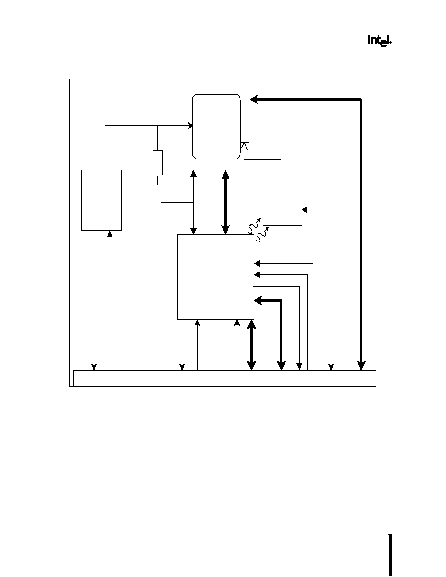
Figure 1 illustrates the block diagram of the Celeron processor mobile module MMC-1.
280-Pin Connector
CPU
Volt. Reg.
PCI Bus
Memory Bus
PCLK1
443DX
V_3
HCLK0
PIIX4E/M Sidebands
ATF
Sense
SMBus
PSB
Mobile
Celeron
Processor
Core
R_GTL
DCLKWR
DCLKRD
GCLKI
GCLKO
SMBus
DCLKO
V_CPUIO 2.5V
V_DC 5V-21V
Processor Core Voltage
Figure 1. Block Diagram of the Celeron Processor Mobile Module MMC-1
3
Celeron
TM
Processor Mobile Module MMC-1
at 466 MHz and 433 MHz
3.0
CONNECTOR INTERFACE
This section provides signal group and connector pin
information. The signals are defined for compatibility with
future Intel mobile modules.
3.1
Signal Definition
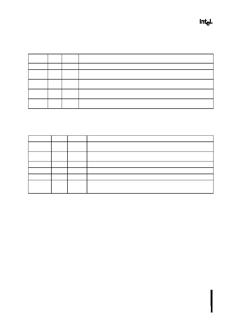
Table 1 provides a list of signals by category and the
corresponding number of signals in each category. For
proper signal termination, please contact your Intel sales
representative for further information.
Table 1. Module Connector Signal Summary
Signal Group
Number of Pins
Memory
108
PCI
56
Processor/PIIX4E/M Sideband
9
Power Management
8
Clocks
8
Voltage: V_DC
10
Voltage: V_3S
20
Voltage: V_5
1
Voltage: V_3
5
Voltage: V_CPUIO
3
JTAG
7
Miscellaneous & Module ID
5
Ground
32
Reserved
8
Total
280

4
Celeron
TM
Processor Mobile Module MMC-1
at 466 MHz and 433 MHz
3.1.1
Signal List
The following notations are used to denote the signal type:
I
Input pin
O
Output pin
O D
Open-drain output pin requiring a pullup resistor
I D
Open-drain input pin requiring a pullup resistor
I/O D
Input/Open-drain output pin, this pin requires a pullup resistor
I/O
Bi-directional input/output pin
The signal description also includes the type of buffer used for a particular signal:
GTL+
Open-drain GTL+ interface signal
PCI
PCI bus interface signals
CMOS
The CMOS buffers are low voltage TTL compatible signals with 3.3-volt outputs and 5.0-volt tolerant inputs.
5
Celeron
TM
Processor Mobile Module MMC-1
at 466 MHz and 433 MHz
3.1.2
Memory (108 Signals)
Table 2 lists the memory interface signals.
Table 2. Memory Signal Descriptions
Name
Type
Voltage
Description
MECC[7:0]
I/O
CMOS
V_3
Memory ECC Data: These signals carry Memory ECC data during access to DRAM.
These pins are not implemented on the MMC-1 connector.
RASA[5:0]# or
CSA[5:0]#
O
CMOS
V_3
Row Address Strobe (EDO): These pins select the DRAM row.
Chip Select (SDRAM): These pins activate the SDRAMs. SDRAM accepts any
command when its CS# pin is active low.
CASA[7:0]# or
DQMA[7:0]
O
CMOS
V_3
Column Address Strobe (EDO): These pins select the DRAM column.
Input/Output Data Mask (SDRAM): These pins act as synchronized output enables
during a read cycle and as a byte mask during a write cycle.
MAB[9:0]#
MAB[10]
MAB[12:11]#
MAB[13]
O
CMOS
V_3
Memory Address (EDO/SDRAM): This is the row and column address for DRAM. The
82443DX Host Bridge system controller has two identical sets of address lines (MAA
and MAB#). The Celeron processor mobile module MMC-1 supports only the MAB set of
address lines. For additional addressing features, please refer to the Intel
Æ
440DX
PCIset Datasheet.
MWE[A, B]#
O
CMOS
V_3
Memory Write Enable (EDO/SDRAM): MWEA# should be used as the write enable for
the memory data bus.
SRAS[A, B]#
O
CMOS
V_3
SDRAM Row Address Strobe (SDRAM): When active low, this signal latches Row
Address on the positive edge of the clock. This signal also allows Row access and pre-
charge.
SCAS[A, B]#
O
CMOS
V_3
SDRAM Column Address Strobe (SDRAM): When active low, this signal latches
Column Address on the positive edge of the clock. This signal also allows Column
access.
CKE[A, B]
O
CMOS
V_3
SDRAM Clock Enable (SDRAM): When these signals are deasserted, SDRAM enters
power-down mode. CKEB is NC and not used by the system electronics.
MD[63:0]
I/O
CMOS
V_3
Memory Data: These signals are connected to the DRAM data bus. They are not
terminated on the Celeron processor mobile module MMC-1.
6
Celeron
TM
Processor Mobile Module MMC-1
at 466 MHz and 433 MHz
3.1.3.
PCI (56 Signals)
Table 3 lists the PCI interface signals.
Table 3. PCI Signal Description
Name
Type
Voltage
Description
AD[31:0]
I/O
PCI
V_3
Address/Data: The standard PCI address and data lines. The address is driven with
FRAME# assertion and data is driven or received in following clocks.
C/BE[3:0]#
I/O
PCI
V_3
Command/Byte Enable: The command is driven with FRAME# assertion and byte
enables corresponding to supplied or requested data is driven on the following clocks.
FRAME#
I/O
PCI
V_3
Frame: Assertion indicates the address phase of a PCI transfer. Negation indicates that
the cycle initiator desires one more data transfer.
DEVSEL#
I/O
PCI
V_3
Device Select: The 82443DX Host Bridge drives this signal when a PCI initiator is
attempting to access DRAM. DEVSEL# is asserted at medium decode time.
IRDY#
I/O
PCI
V_3
Initiator Ready: Asserted when the initiator is ready for data transfer.
TRDY#
I/O
PCI
V_3
Target Ready: Asserted when the target is ready for data transfer.
STOP#
I/O
PCI
V_3
Stop: Asserted by the target to request the master to stop the current transaction.
PLOCK#
I/O
PCI
V_3
Lock: Indicates an exclusive bus operation and may require multiple transactions to
complete. When LOCK# is asserted, nonexclusive transactions may proceed. The
82443DX supports lock for CPU initiated cycles only. PCI initiated locked cycles are not
supported.
REQ[4:0]#
I
PCI
V_3
PCI Request: PCI master requests for PCI.
GNT[4:0]#
O
PCI
V_3
PCI Grant: Permission is given to the master to use PCI.
PHOLD#
I
PCI
V_3
PCI Hold: This signal comes from the expansion bridge; it is the bridge request for PCI.
The 82443DX Host Bridge will drain the DRAM write buffers, drain the processor-to-PCI
posting buffers, and acquire the host bus before granting the request via PHLDA#. This
ensures that GAT timing is met for ISA masters. The PHOLD# protocol has been
modified to include support for passive release.
PHLDA#
O
PCI
V_3
PCI Hold Acknowledge: The 82443DX Host Bridge drives this signal to grant PCI to
the expansion bridge. The PHLDA# protocol has been modified to include support for
passive release.
PAR
I/O
PCI
V_3
Parity: A single parity bit is provided over AD[31:0] and C/BE[3:0]#.
SERR#
I/O
PCI
V_3
System Error: The 82443DX asserts this signal to indicate an error condition. Please
refer to the Intel
Æ
440BX PCIset Datasheet for further information.
CLKRUN#
I/O D
PCI
V_3
Clock Run: An open-drain output and input. The 82443DX Host Bridge requests the
central resource (PIIX4E/M) to start or maintain the PCI clock by asserting CLKRUN#.
The 82443DX Host Bridge tri-states CLKRUN# upon deassertion of Reset (since CLK is
running upon deassertion of Reset).
PCI_RST#
I
CMOS
V_3
Reset: When asserted, this signal asynchronously resets the 82443DX Host Bridge.
The PCI signals also tri-state, compliant with the PCI Rev 2.1 specifications .
3.1.4
Processor and PIIX4E/M Sideband (9
Signals)
Table 4 lists the processor and PIIX4E/M sideband interface
signals. The voltage level for these signals is determined by
V_CPUIO.
7
Celeron
TM
Processor Mobile Module MMC-1
at 466 MHz and 433 MHz
Table 4. Processor/PIIX4E/M Sideband Signal Descriptions
Name
Type
Voltage Description
FERR#
O
CMOS
V_CPUIO
Numeric Coprocessor Error: This pin functions as a FERR# signal supporting
coprocessor errors. This signal is tied to the coprocessor error signal on the processor
and is driven by the processor to the PIIX4E/M.
CPURST
N/C
CMOS
V_CPUIO
Processor Reset: The signal is not used in the Celeron processor mobile module
MMC-1.
IGNNE#
ID
CMOS
V_CPUIO
Ignore Error: This open-drain signal is connected to the Ignore Error pin on the
processor and is driven by the PIIX4E/M.
INIT#
ID
CMOS
V_CPUIO
Initialization: INIT# is asserted by the PIIX4E/M to the processor for system
initialization. This signal is an open-drain.
INTR
ID
CMOS
V_CPUIO
Processor Interrupt: INTR is driven by the PIIX4E/M to signal the processor that an
interrupt request is pending and needs to be serviced. This signal is an open-drain.
NMI
ID
CMOS
V_CPUIO
Non-Maskable Interrupt: NMI is used to force a non-maskable interrupt to the
processor. The PIIX4E/M ISA bridge generates NMI when either SERR# or IOCHK# is
asserted, depending on how the NMI Status and Control Register is programmed. This
signal is an open-drain.
A20M#
ID
CMOS
V_CPUIO
Address Bit 20 Mask: When enabled, this open-drain signal causes the processor to
emulate the address wraparound at 1 MB, which occurs on the Intel 8086 processor.
SMI#
ID
CMOS
V_CPUIO
System Management Interrupt: SMI# is an active low synchronous output from the
PIIX4E/M that is asserted in response to one of many enabled hardware or software
events. The SMI# open-drain signal can be an asynchronous input to the processor.
However, in this chip set SMI# is synchronous to PCLK.
STPCLK#
ID
CMOS
V_CPUIO
Stop Clock : STPCLK# is an active low synchronous open-drain output from the
PIIX4E/M that is asserted in response to one of many hardware or software events.
STPCLK# connects directly to the processor and is synchronous to PCICLK. When the
processor samples STPCLK# asserted, it responds by entering a low power state (Quick
Start). The processor will only exit this mode when this signal is deasserted.

8
Celeron
TM
Processor Mobile Module MMC-1
at 466 MHz and 433 MHz
3.1.5
Power Management (8 Signals)
Table 5 lists the power management interface signals. The
SM_CLK and SM_DATA signals refer to the two-wire serial
SMBus interface. Although this interface is currently used
solely for the digital thermal sensor, the SMBus contains
reserved serial addresses for future use. See section 4.9 for
more details.
Table 5. Power Management Signal Descriptions
Name
Type
Voltage
Description
OEM_PU
I
CMOS
V_3
OEM Pullup: This pullup resistor is not required on the Celeron processor mobile
module MMC-1.
L2_ZZ
N/C
CMOS
V_CPUIO
Low-Power Mode For Cache SRAM: This signal is not used on the Celeron
processor mobile module MMC-1.
SUS_STAT#
I
CMOS
V_3ALWAYS
1
Suspend Status: This signal connects to the SUS_STAT1# outputs of PIIX4E/M. It
provides information on host clock status and is asserted during all suspend states.
VR_ON
I
V_3
VR_ON: Voltage regulator ON. This 3.3V (5V tolerant) signal controls the operation
of the voltage regulator. VR_ON should be generated as a function of the PIIX4E/M
SUSB# signal, which is used for controlling the "Suspend State B" voltage planes.
This signal should be driven by a digital signal with a rise/fall time of less than or
equal to 1 us. (VIL(max)=0.4V, VIH(min)=3.0V). See Figure 5, "Power-on Sequence
Timing" for proper sequencing of VR_ON.
VR_PWRGD
O
V_3
VR_PWRGD: This signal is driven high to indicate that the voltage regulator is
stable and is pulled low using a 100K resistor when inactive. It can be used in some
combination to generate the system PWRGOOD signal.
SM_CLK
I/O D
CMOS
V_3
Serial Clock: This clock signal is used on the SMBus interface to the digital thermal
sensor. Ensure proper termination based upon the System Management Bus
Specification, Revision 1.0.
SM_DATA
I/O D
CMOS
V_3
Serial Data: An open-drain data signal on the SMBus interface to the digital thermal
sensor. Ensure proper termination based upon the System Management Bus
Specification, Revision 1.0.
ATF_INT#
O D
CMOS
V_3
ATF Interrupt: This signal is an open-drain output signal of the digital thermal
sensor.
NOTE:
V_3ALWAYS: 3.3V supply. It is generated whenever V_DC is available and supplied to PIIX4E/M resume well.
9
Celeron
TM
Processor Mobile Module MMC-1
at 466 MHz and 433 MHz
3.1.6
Clock (8 Signals)
Table 6 lists the clock interface signals.
Table 6. Clock Signal Descriptions
Name
Type
Voltage
Description
OEM_PD
I
CMOS
V_3
OEM Pulldown: It is renamed from PCI_REF and is not required on the module.
PCLK
I
PCI
V_3S
PCI Clock In: PCLK is an input to the module from the CKDM66-M clock source and is
one of the system's PCI clocks. This clock is used by all of the 82443DX Host Bridge
logic in the PCI clock domain. This clock is stopped when the PIIX4E/M PCI_STP#
signal is asserted and/or during all suspend states.
HCLK[1:0]
I
CMOS
V_CPUIO
Host Clock In: These clocks are inputs to the module from the CKDM66-M clock source
and are used by the processor and the 82443DX Host Bridge system controller. This
clock is stopped when the PIIX4E/M CPU_STP# signal is asserted and/or during all
suspend states.
SUSCLK
N/C
CMOS
V_3
Suspend Clock : This signal is not used on the module.
FQS[1:0]
O
CMOS
V_3S
Frequency Status: This signal provides the status of the host clock frequency to the
system electronics. These signals are static and are pulled either low or high to the
V_3S voltage supply through a 10-K
resistor. This module is designed for the 66-MHz
strapping option shown below.
FQS1
FQS0
Frequency
0
0
60 MHz
0
1
66 MHz
1
0
Reserved
1
1
Reserved
CPU3.3_2.5#
O
CMOS
V_CPUIO
Clock Voltage Select: Provides status to the system electronics about the voltage level
at which the CKDM66-M clock generator should be operating. This signal is pulled low
by module.
10
Celeron
TM
Processor Mobile Module MMC-1
at 466 MHz and 433 MHz
3.1.7
Voltages (39 Signals)
Table 7 lists the voltage signal definitions.
Table 7. Voltage Descriptions
Name
Type
Number
of Pins
Description
V_DC
I
10
DC Input: 5V-21V.
V_3S
I
20
SUSB# controlled 3.3V: V_3S is supplied by the system electronics. This is a 3.3V power
supply that is turned off during suspend during system states STR, STD, and Soff.
V_5
I
1
SUSC# controlled 5V: Power managed 5V supply. An output of the voltage regulator on the
system electronics. This rail is off during STD and Soff.
V_3
I
5
SUSC# controlled 3.3V: Power managed 3.3V supply. An output of the voltage regulator on
the system electronics. This rail is off during STD and Soff.
V_CPUIO
O
3
Processor I/O Ring: Powers the processor interface signals such as the PIIX4E/M open-drain
pullups for the processor/PIIX4E/M sideband signals and the CKDM66-M clock source.
3.1.8
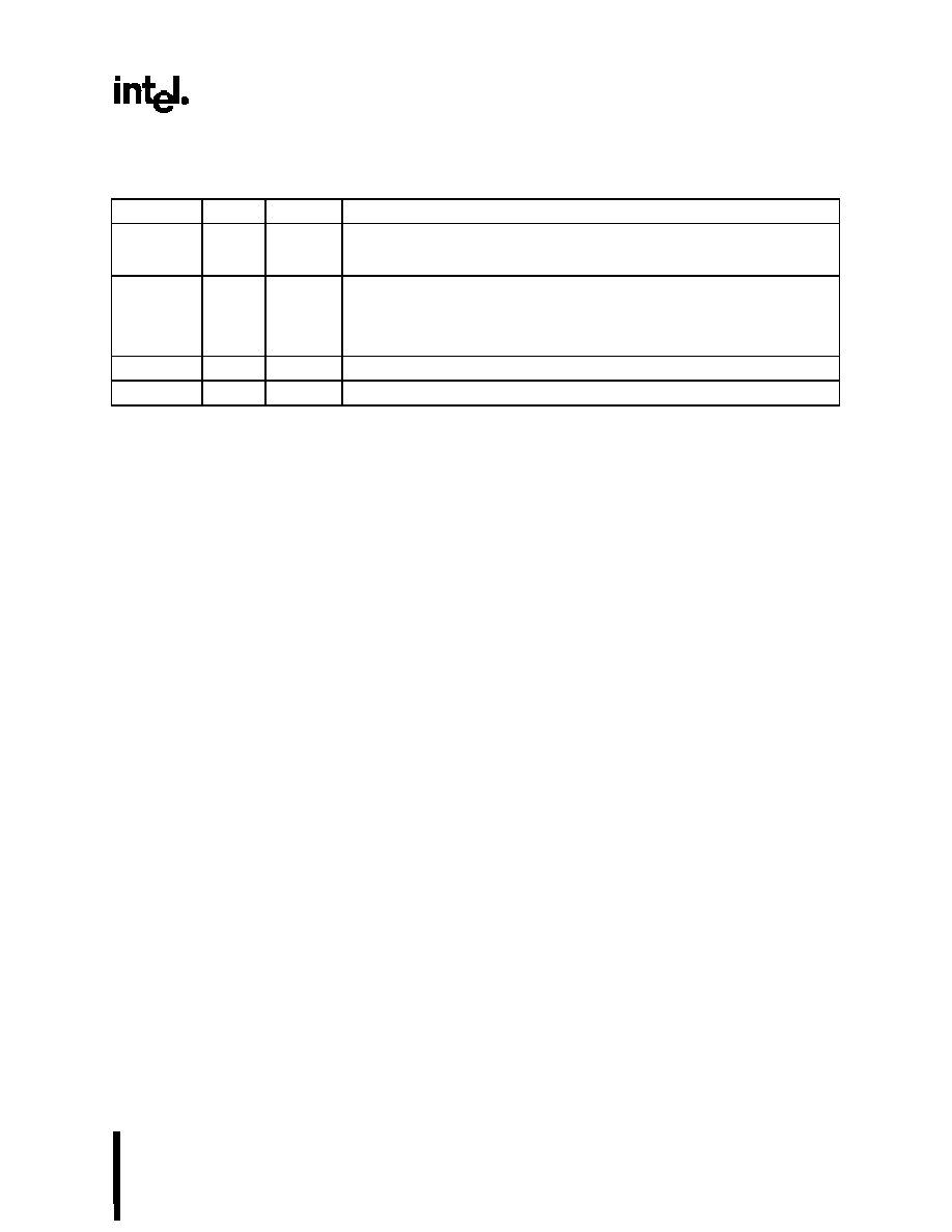
JTAG (7 Signals)
Table 8 lists the JTAG signals, which the system electronics
can use to implement a JTAG chain and ITP port, if desired.
The JTAG signals provided cannot be used as an ITP port,
since the ITP interface has changed between the
generations of the mobile Pentium processor and the mobile
Celeron processor.
Table 8. JTAG Pins
Name
Type
Voltage
Description
TDO
O
V_CPUIO
JTAG Test Data Out: Serial output port. TAP instructions and data is shifted out of the
processor from this port.
TDI
I
V_CPUIO
JTAG Test Data In: Serial input port. TAP instructions and data is shifted into the
processor from this port.
TMS
I
V_CPUIO
JTAG Test Mode Select: Controls the TAP controller change sequence.
TCLK
I
V_CPUIO
JTAG Test Clock: Testability clock for clocking the JTAG boundary scan sequence.
TRST#
I
V_CPUIO
JTAG Test Reset: Asynchronously resets the TAP controller in the processor.
ITP(1:0)
ITP1
ITP0
O
I
V_CPUIO
Debug Port Signals: These signals are not used in the Celeron processor mobile
module MMC-1and should not be connected.
NOTE:
DBREST# (reset target system) on the ITP debug port can be "logically ANDed" with VR_PWRGD TO PIIX4E/M's PWROK.
11
Celeron
TM
Processor Mobile Module MMC-1
at 466 MHz and 433 MHz
3.1.9
Miscellaneous (45 Signals)
Table 9 lists the miscellaneous signals.
Table 9. Miscellaneous Pins
Name
Type
Number
Description
Module
ID[3:0]
O
CMOS
4
Module Revision ID: These pins track the revision level of the module. A 100-K pullup
resistor to V_3S is required on these signals and should be placed on the system
electronics. See Section 7.0 for more detail.
PPP_PP#
O
CMOS
1
Mobile Celeron processor or mobile Pentium processor present: A high on this
signal indicates to the PIIX4E/M ISA bridge CONFIG1 pin that the module is based on
the Pentium Pro architecture. A low indicates that the module is of the Pentium
processor family. This signal is allowed to float on the module and requires a 100-K
pullup resistor to V_3S on the system electronics. This signal is grounded.
Ground
I
32
Ground.
Reserved
RSVD
8
Unallocated Reserved pins and should not be connected.
12
Celeron
TM
Processor Mobile Module MMC-1
at 466 MHz and 433 MHz
3.2
Connector Pin Assignments
Table 10 lists the signals for each pin of the MMC-1 to the
notebook manufacturer's system electronics. Refer to
section 3.3, "Pin and Pad Assignments" for the pin
assignments of the pads on the connector.
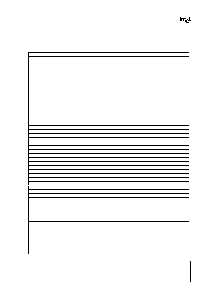
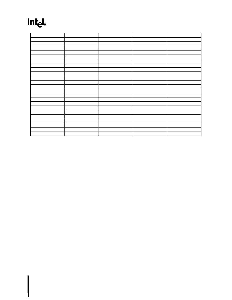
Table 10. Connector Pin Assignments
Pin Number
Row
Row
Row
Row
AA
AB
BA
BB
1
Gnd
Gnd
Gnd
Gnd
2
MD31
MD63
MID0
MID1
3
MD30
MD61
Reserved
Reserved
4
MD29
MD62
V_DC
V_DC
5
MD27
MD58
V_DC
V_DC
6
V_3S
V_3S
V_DC
V_DC
7
MD28
MD60
V_DC
V_DC
8
MD26
MD56
V_DC
V_DC
9
MD25
MD57
Reserved
Reserved
10
MD24
MD59
MID2
MID3
11
Gnd
Gnd
Gnd
Gnd
12
CAS3#/DQM3
CAS7#/DQM7
AD00
FRAME#
13
CAS6#/DQM6
CAS2#/DQM2
AD01
LOCK#
14
MA00
MA01
AD02
DEVSEL#
15
CKEA
CKEB
AD03
IRDY#
16
V_3S
V_3S
V_3S
V_3S
17
MA02
MA04
AD04
TRDY#
18
MA03
MA05
AD05
STOP#
19
MD55
MD22
AD06
PHOLD#
20
MD54
MD23
AD07
PHLDA#
21
Gnd
Gnd
Gnd
Gnd
22
MD51
MD20
AD08
PCI_RST#
23
MD52
MD21
AD09
PAR
24
MD53
MD19
AD10
SERR#
25
MD49
MD17
AD11
REQ0#
26
V_3S
V_3S
V_3S
REQ1#
27
MD48
MD18
AD12
REQ2#
28
MD50
MD16
AD13
REQ3#
29
SRASA#
SCASA#
AD14
GNT0#
30
SRASB#
SCASB#
AD15
GNT1#
31
Gnd
Gnd
Gnd
Gnd
32
MWEA#
MECC3
AD16
GNT2#
33
MWEB#
MECC7
AD17
GNT3#
34
RAS0#/CS0#
MECC6
AD18
L2_ZZ
35
RAS1#/CS1#
MECC2
AD19
Reserved
36
V_3S
V_3S
V_3S
V_3S
37
MD14
MECC1
AD20
Reserved
38
MD11
MECC5
AD21
PPP_PP#
39
MD15
MECC4
AD22
CLKRUN#
40
Gnd
Gnd
Gnd
Gnd
41
MD10
MECC0
RAS2#/CS2#
SM_CLK
42
MD13
MD43
RAS3#/CS3#
SM_DATA
43
MD09
MD41
RAS4#/CS4#
ATF_INT#
44
MD08
MD45
RAS5#/CS5#
SUSCLK
45
V_3S
V_3S
V_3
V_3
Row
Row
Row
Row
AA
AB
BA
BB
46
MD12
MD42
AD23
SUS_STAT#
13
Celeron
TM
Processor Mobile Module MMC-1
at 466 MHz and 433 MHz
47
MA06
MD40
AD24
V_3
48
MA07
MD44
AD25
OEM_PU
49
MA08
MD46
AD26
VR_ON
50
Gnd
Gnd
Gnd
Gnd
51
MA09
MD47
AD27
VR_PWRGD
52
CAS1#/DQM1
CAS5#/DQM5
AD28
V_3
53
CAS4#/DQM4
CAS0#/DQM0
AD29
V_3
54
MA10
MA12
AD30
Reserved
55
V_3S
V_3S
V_3S
Reserved
56
MA11
MA13
AD31
INIT#
57
MD39
MD07
C/BE0#
V_CPUIO
58
MD37
MD02
C/BE1#
INTR
59
MD38
MD00
C/BE2#
CPURST
60
Gnd
Gnd
Gnd
Gnd
61
MD36
MD04
C/BE3#
STPCLK#
62
MD33
MD01
IGNNE#
SMI#
63
MD35
MD03
FERR#
NMI
64
MD32
MD06
A20M#
V_5
65
MD34
MD05
V_CPUIO
V_CPUIO
66
V_3S
V_3S
TDO
TRST#
67
OEM_PD
PCLK
ITP0
TDI
68
FQS0
FQS1
ITP1
TMS
69
HCLK1
HCLK0
CPU3.3_2.5#
TCLK
70
Gnd
Gnd
Gnd
Gnd
14
Celeron
TM
Processor Mobile Module MMC-1
at 466 MHz and 433 MHz
3.3
Pin and Pad Assignments
The MMC-1 surface mount connector has a 0.6-milimeter
pitch and has 280 pins. For size information, refer to section
5.1.4 "Height Restrictions". Figure 2 shows the connector
pad assignments for the manufacturer's system electronics.
AA 70
AA 1
AB 70
AB 1
BA 70
BA 1
BB 70
BB 1
Figure 2. 280-Pin Connector Footprint Pad Numbers, Module Secondary Side
15
Celeron
TM
Processor Mobile Module MMC-1
at 466 MHz and 433 MHz
Table 11 summarizes the key specifications for the MMC-1 connector.
Table 11. Connector Specifications
Parameter
Condition
Specification
Material
Contact
Copper Alloy
Housing
Thermo Plastic Molded Compound: LCP
Electrical
Current
0.5 A
Voltage
50 VAC
Insulation Resistance
100 M
minimum at 200 VDC
Termination Resistance
50 m
maximum
Capacitance
5 pF maximum per contact
Mechanical
Mating Cycles
50 cycles
Connector Mating Force
3.2 oz per contact
Contact Unmating Force
0.35 oz per contact
4.0
FUNCTIONAL DESCRIPTION
4.1
Celeron Processor Mobile Module MMC-1
The Celeron processor mobile module MMC-1 is offered at
speeds of 466 megahertz and 433 megahertz. All processor
speeds have a PSB speed of 66 megahertz.
4.2
L2 Cache
The on-die L2 cache is 128 kilobytes, is four-way set
associative, and runs at the speed of the processor core.
4.3
The 82443DX Host Bridge System
Controller
Intel's 82443DX Host Bridge system controller combines the
mobile Celeron processor bus controller, the DRAM
controller, and the PCI bus controller into one component.
The 82443DX Host Bridge has multiple power management
features designed specifically for notebook systems such as:
∑
CLKRUN#, a feature that enables controlling of the PCI
clock on or off.
∑
The 82443DX Host Bridge suspend modes, which
include Suspend-to-RAM (STR), Suspend-to-Disk
(STD), and Powered-On-Suspend (POS).
∑
System Management RAM (SMRAM) power
management modes, which include Compatible
SMRAM (C_SMRAM) and Extended SMRAM
(E_SMRAM). C_SMRAM is the traditional SMRAM
feature implemented in all Intel PCI chipsets.
E_SMRAM is a new feature that supports write-back
cacheable SMRAM space up to 1 megabyte. To
minimize power consumption while the system is idle,
the internal 82443DX Host Bridge clock is turned off
(gated off). This is accomplished by setting the G_CLK
enable bit in the power management register in the
82443DX through the system BIOS.
4.3.1
Memory Organization
The MMC-1 connector signaling interface supports the
82443DX Host Bridge standard mode, memory
configurations, and modes of operation. This allows the
memory interface to support the following:
∑
One set of memory control signals, sufficient to support
up to three SO-DIMM sockets and six banks of SDRAM
at 66 megahertz.
∑
One CKE signal for each bank.
Memory features not supported by the 82443DX Host Bridge
system controller standard MMC-1 mode are:
∑
Support for eight banks of memory.
∑
Second set of memory address lines (MAA[13:0]).
∑
Accelerated Graphics Port (AGP).
The 82443DX Host Bridge system controller supports DRAM
technologies EDO and SDRAM. These memory types should
not be mixed in the system, so that all DRAM in all rows
(RAS[5:0]#) must be of the same technology. The 82443DX
Host Bridge system controller targets 60-nanosecond EDO
DRAMs, and 66-megahertz SDRAMs.
The Celeron processor mobile module's clocking
architecture supports the use of SDRAM. Tight timing
requirements of the 66-megahertz SDRAM clocks allow all
host and SDRAM clocks to be generated from the same
clocking architecture on the OEM's system electronics. For
complete details about using SDRAM memory and for trace
length guidelines, refer to the Mobile PentiumÆ II processor /
82443BX PCIset Advanced Platform Recommended Design
and Debug Practices. Refer to the Intel
Æ
440BX PCIset
Datasheet for details on memory device support,
organization, size, and addressing.
4.3.2
Reset Strap Options
Several strap options on the memory address bus define the
behavior of the Celeron processor mobile module
MMC-1after reset. Other straps are allowed to override the
default settings. Table 14 shows the various straps and their
implementation.
16
Celeron
TM
Processor Mobile Module MMC-1
at 466 MHz and 433 MHz
Table 12. Configuration Straps for the 82443DX Host Bridge System Controller
Signal
Function
Module Default Setting
MAB[12]#
Host Frequency
Select
No strap
-
66-MHz default.
MAB[11]#
In order queue depth
No strap
-
maximum queue depth is set, i.e. 8.
MAB[10]
Quick Start select
Strapped high on the module for Quick Start mode.
MAB[9]#
AGP disable
Strapped to disable AGP.
MAB[7]#
MM Config
Strapped for MMC-1 compatible mode.
MAB[6]#
Host Bus Buffer Mode
select
Strapped high on the module for mobile PSB buffers.
4.3.3
PCI Interface
The PCI interface of the 82443DX Host Bridge is available at
the connector. The 82443DX Host Bridge supports the PCI
Clockrun protocol for PCI bus power management. In this
protocol, PCI devices assert the CLKRUN# open-drain
signal when they require the use of the PCI interface. Refer
to the PCI Mobile Design Guide for complete details on the
PCI Clockrun protocol.
The 82443DX Host Bridge is responsible for arbitrating the
PCI bus. With the MMC-1 connector the 82443DX Host
Bridge can support up to five PCI bus masters. There are
five PCI Request/Grant pairs, REQ[4:0]# and GNT[4:0]#,
available to the manufacturer's system electronics.
The PCI interface on the connector is 3.3 volts only. All
devices that drive outputs to a 5.0
Vt
nominal V
oh
level are not
supported.
The 82443DX Host Bridge system controller is compliant
with the PCI 2.1 specification, which improves the worst
case PCI bus access latency from earlier PCI specifications.
As detailed in the PCI specification, the 82443DX Host
Bridge supports only Mechanism #1 for accessing PCI
configuration space. This implies that signals AD[31:11] are
available for PCI IDSEL signals. However, since the
82443DX Host Bridge is always device #0, AD11 will never
be asserted during PCI configuration cycles as an IDSEL.
The 82443DX reserves AD12 for the AGPbus, which is not
supported by the MMC-1 connector. Thus, AD13 is the first
available address line usable as an IDSEL. AD18 should be
used by the PIIX4E/M.
4.3.4
AGP Feature Set
The Intel MMC-1 family does not support the AGP graphics
port interface. For AGP information, refer to the Intel
Æ
Celeron
TM
Processor Mobile Module: Mobile Module
Connector 2 (MMC-2).
4.4
Power Management
4.4.1
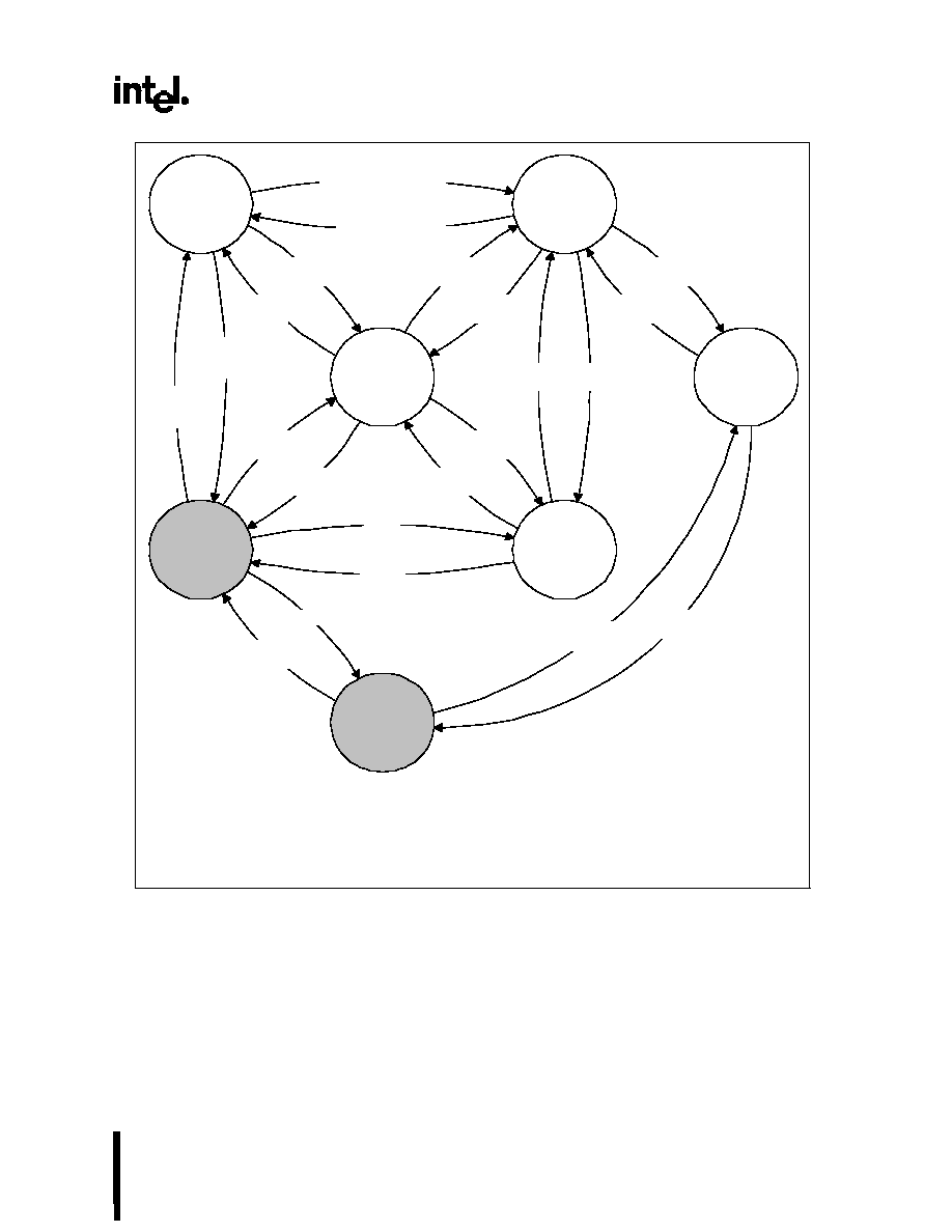
Clock Control Architecture
The Celeron processor mobile module's clock control
architecture is optimal for notebook designs. The clock
control architecture consists of seven different clock states:
Normal, Stop Grant, Auto Halt, Quick Start, HALT/Grant
Snoop, Sleep, and Deep Sleep. The Auto Halt state provides
a low power clock state that can be controlled through the
software execution of the HLT instruction. The Quick Start
state provides a low power, low exit latency clock state that
can be used for hardware controlled "idle" computer states.
The Deep Sleep state provides an extremely low power state
that can be used for "Power-on Suspend" states, which is an
alternative to shutting off the processor's power.
The exit latency of the Deep Sleep state has been reduced
to 30 microseconds. The Stop Grant and Sleep states are
not available on the Celeron processor mobile module as
these states are intended for desktop or server systems. The
Stop Grant and the Quick Start clock states are mutually
exclusive. For example a strapping option on signal A15#
chooses which state is entered when the STPCLK# signal is
asserted. Strapping the A15# signal to ground at Reset
enables the Quick Start state. Otherwise, asserting the
STPCLK# signal puts the mobile Celeron processor into the
Stop Grant state. The Stop Grant state is useful for SMP
platforms and is not supported on the Celeron processor
mobile module MMC-1. The Quick Start state is available on
the module and provides a significantly lower power level.
Figure 3 provides an illustration of the clocking architecture.
Performing state transitions not shown in Figure 3 is neither
recommended nor supported.
.
17
Celeron
TM
Processor Mobile Module MMC-1
at 466 MHz and 433 MHz
HALT/Grant
Snoop
Normal
State
HS=false
Stop
Grant
Auto
Halt
HS=true
Quick
Start
Sleep
Deep
Sleep
(!STPCLK#
and !HS) or
stop break
STPCLK# and
!QSE and SGA
Snoop
occurs
Snoop
serviced
STPCLK# and
QSE and SGA
(!STPCLK# and !HS)
or RESET#
Snoop
serviced
Snoop
occurs
!STPCLK#
and HS
STPCLK# and
!QSE and SGA
HLT and
halt bus cycle
halt
break
Snoop
serviced
Snoop
occurs
STPCLK# and
QSE and SGA
!STPCLK#
and HS
!SLP# or
RESET#
SLP#
BCLK
stopped
BCLK on
and !QSE
BCLK
stopped
BCLK on
and QSE
Halt break ≠ A20M#, BINIT#, FLUSH#, INIT#, INTR, NMI, PREQ#, RESET#, SMI#
HLT ≠ HLT instruction executed
HS ≠ Processor Halt State
QSE ≠ Quick Start State Enabled
SGA ≠ Stop Grant Acknowledge bus cycle issued
Stop break ≠ BINIT#, FLUSH#, RESET#
Intel mobile modules do not support the shaded clock control states
Figure 3. Clock Control States

18
Celeron
TM
Processor Mobile Module MMC-1
at 466 MHz and 433 MHz
4.4.2
Normal State
This is the normal operating mode. The processor's core
clock is running and the processor is actively executing
instructions.
4.4.3
Auto Halt State
This is a low power mode entered by the processor through
the execution of the HLT instruction. The power level of this
mode is similar to the Stop Grant state. A transition to the
Normal state is made by a halt break event (one of the
following signals going active: NMI, INTR, BINIT#, INIT#,
RESET#, FLUSH#, or SMI#).
Asserting the STPCLK# signal while in the Auto Halt state
will cause the processor to transition to the Stop Grant or
Quick Start state, which issues a Stop Grant Acknowledge
bus cycle. Deasserting STPCLK# will cause the processor to
return to the Auto Halt state without issuing a new Halt bus
cycle.
The SMI# (System Management Interrupt) is recognized in
the Auto Halt state. Returning from the SMI handler can be
to either the Normal state or the Auto Halt state. See the
Intel
Æ
Architecture Software Developer's Manual, Volume
III: System Programmer's Guide for more information. No
Halt bus cycle is issued when returning to the Auto Halt state
from System Management Mode (SMM).
The FLUSH# signal is serviced in the Auto Halt state. After
flushing the on-chip, the processor will return to the Auto
Halt state without issuing a Halt bus cycle. Transitions in the
A20M# and PREQ# signals are recognized while in the Auto
Halt state.
4.4.4
Stop Grant State
Intel mobile modules do not support the Stop Grant state.
The processor enters this mode with the assertion of the
STPCLK# signal when it is configured for Stop Grant state
(via the A15# strapping option). The processor still responds
to snoop requests and latch interrupts. Latched interrupts will
be serviced when the processor returns to the Normal state.
Only one occurrence of each interrupt event will be latched.
A transition back to the Normal state can be made by the
deassertion of the STPCLK# signal or the occurrence of a
stop break event (a BINIT#, FLUSH#, or RESET# assertion).
The processor will return to the Stop Grant state after the
completion of a BINIT# bus initialization unless STPCLK#
has been deasserted. RESET# assertion will cause the
processor to immediately initialize itself, but the processor
will stay in the Stop Grant state after initialization until
STPCLK# is deasserted. If the FLUSH# signal is asserted,
the processor will flush the on-chip caches and return to the
Stop Grant state. A transition to the Sleep state can be made
by the assertion of the SLP# signal.
While in the Stop Grant state, assertions of SMI#, INIT#,
INTR, and NMI (or LINT[1:0]) will be latched by the
processor. These latched events will not be serviced until the
processor returns to the Normal state. Only one of each
event will be recognized upon return to the Normal state.
4.4.5
Quick Start State
This is a mode entered by the processor with the assertion
of the STPCLK# signal when it is configured for the Quick
Start state (via the A15# strapping option). In the Quick Start
state the processor is only capable of acting on snoop
transactions generated by the PSB priority device. Because
of its snooping behavior, Quick Start can only be used in
single processor configurations.
A transition to the Deep Sleep state can be made by
stopping the clock input to the processor. A transition back to
the Normal state (from the Quick Start state) is made only if
the STPCLK# signal is deasserted.
While in this state the processor is limited in its ability to
respond to input. It is incapable of latching any interrupts,
servicing snoop transactions from symmetric bus masters, or
responding to FLUSH# or BINIT# assertions. While the
processor is in the Quick Start state, it will not respond
properly to any input signal other than STPCLK#, RESET#,
or BPRI#. If any other input signal changes, then the
behavior of the processor will be unpredictable. No serial
interrupt messages may begin or be in progress while the
processor is in the Quick Start state.
RESET# assertion will cause the processor to immediately
initialize itself, but the processor will stay in the Quick Start
state after initialization until STPCLK# is deasserted.
4.4.6
HALT/Grant Snoop State
The processor will respond to snoop transactions on the
PSB while in the Auto Halt state, the Stop Grant state, or the
Quick Start state. When a snoop transaction is presented on
the PSB the processor will enter the HALT/Grant Snoop
state. The processor will remain in this state until the snoop
has been serviced and the PSB is quiet. After the snoop has
been serviced, the processor will return to its previous state.
If the HALT/Grant Snoop state is entered from the Quick
Start state, then the input signal restrictions of the Quick
Start state still apply in the HALT/Grant Snoop state, except
for those signal transitions that are required to perform the
snoop.
4.4.7
Sleep State
Intel mobile modules do not support the Sleep state.
The Sleep state is a very low power state in which the
processor maintains its context and the phase-locked loop
(PLL) maintains phase lock. The Sleep state can only be
entered from the Stop Grant state. After entering the Stop
Grant state the SLP# signal can be asserted, causing the
processor to enter the Sleep state. The SLP# signal is not
recognized in the Normal state or the Auto Halt state.
The processor can be reset by the RESET# signal while in
the Sleep state. If RESET# is driven active while the
processor is in the Sleep state, then SLP# and STPCLK#
must immediately be driven inactive to ensure that the
processor correctly initializes itself.
Input signals (other than RESET#) may not change while the
processor is in the Sleep state or transitioning into or out of
the Sleep state. Input signal changes at these times will
cause unpredictable behavior. Thus, the processor is
incapable of snooping or latching any events in the Sleep
state.
While in the Sleep state the processor can enter its lowest
power state, the Deep Sleep state. Removing the
19
Celeron
TM
Processor Mobile Module MMC-1
at 466 MHz and 433 MHz
processor's input clock puts the processor in the Deep Sleep
state. PICCLK may be removed in the Sleep state.
4.4.8
Deep Sleep State
The Deep Sleep state is the lowest power mode the
processor can enter while maintaining its context. Stopping
the BCLK input to the processor enters Sleep state. For
proper operation, the BCLK input should be stopped in the
low state.
The processor will return to the Sleep state or the Quick
Start state from the Deep Sleep state when the BCLK input
is restarted. Due to the PLL lock latency, there is a 30-
millisecond delay after the clocks have started before this
state transition happens. PICCLK may be removed in the
Deep Sleep state. PICCLK should be designed to turn on
when BCLK turns on when transitioning out of the Deep
Sleep state.
The input signal restrictions for the Deep Sleep state are the
same as for the Sleep state, except that RESET# assertion
will result in unpredictable behavior.
Table 13. Clock State Characteristics
Clock
State
Exit Latency
Processor
Power
Snooping
System Uses
Normal
N/A
Varies
Yes
Normal program execution
Auto Halt
Approximately 10 bus clocks
1.2W
Yes
S/W controlled entry idle mode
Stop Grant
1
10 bus clocks
1.2W
Yes
H/W controlled entry/exit mobile throttling
Quick Start
Through snoop, to HALT/Grant Snoop
state: immediate
Through STPCLK#, to Normal state:
10 bus clocks
0.5W
Yes
H/W controlled entry/exit mobile throttling
HALT/Grant
Snoop
1
A few bus clocks after the end of
snoop activity.
Not
specified
Yes
Supports snooping in the low power
states
Sleep
To Stop Grant state 10 bus clocks
0.5W
No
H/W controlled entry/exit desktop idle
mode support
Deep Sleep
30 msec
150 mW
No
H/W controlled entry/exit mobile
powered-on suspend support
NOTES:
1.
Intel mobile modules do not support shaded clock control states.
2.
Not 100% tested. Specified at 50
∞
C by design/characterization.
4.5
Typical POS/STR Power
Table 14 lists the POS/STR typical power specifications.
Table 14. POS/STR Power
State
Typical MMC-1 Power
POS
0.475W
STR
0.018W
NOTE:
These are average values of measurement and are guidelines only.
4.6
Electrical Requirements
The following section provides information on the electrical
requirements for the Celeron processor mobile module
MMC-1.
4.6.1
DC Requirements
Table 15 provides DC power supply design criteria.
Table 15. Power Supply Design Specifications
1
Symbol
Parameter
Min
Nom
Max
Unit
Notes
V
DC
2,3
DC Input Voltage
5.0
12.0
21.0
V
I
DC
DC Input Current
0.1
0.9
3.5
A
I
DC-Surge
Maximum Surge Current for V
DC
17.3
A
20
Celeron
TM
Processor Mobile Module MMC-1
at 466 MHz and 433 MHz
Symbol
Parameter
Min
Nom
Max
Unit
Notes
I
DC-Leakage
4
Typical Leakage Current for V
DC
4.0
µ
A
(at 25
∞
C)
V
5
Power Managed 5V Voltage Supply
4.75
5.0
5.25
V
I
5
Power Managed 5V Current
17
32
60
mA
I
5-Surge
Maximum Surge Current for V
5
0.6
A
I
5-Leakage
Typical Leakage Current for V
5
1.0
µ
A
V
3
Power Managed 3.3V Voltage Supply
3.135
3.3
3.465
V
I
3
Power Managed 3.3V Current
0.8
1.2
2.0
A
I
3-Surge
Maximum Surge Current for V
3
2.8
A
I
3-Leakage
Typical Leakage Current for V
3
1.1
mA
V
3S
Power Managed 3.3V Voltage Supply
3.135
3.3
3.465
V
I
3S
Power Managed 3.3V Current
0.35
0.5
mA
I
3S-Surge
Maximum Surge Current for V
3S
TBD
A
I
3S-Leakage
Typical Leakage Current for V
3S
TBD
TBD
TBD
mA
V
CPUPU
Processor I/O Ring Voltage
2.375
2.5
2.625
V
±
0.125
I
CPUPU
5
Processor I/O Ring Current
0
10
20
mA
V
CLK
Processor Clock Rail Voltage
2.375
2.5
2.625
V
±
0.125
I
CLK
5
Processor Clock Rail Current
24.0
35.0
80.0
mA
NOTES:
1.
Unless otherwise noted, all specifications in this table apply to all Intel mobile module frequencies.
2.
V_DC is set for 12V in order to determine typical V_DC current.
3.
V_DC is set for 5V in order to determine maximum V_DC current.
4.
Leakage current that can be expected when VR_ON is deactivated and V_DC is still applied.
5.
These values are system dependent.
21
Celeron
TM
Processor Mobile Module MMC-1
at 466 MHz and 433 MHz
4.6.2
AC Requirements
Table 16 provides the PSB clock (BCLK) AC requirements
for the Celeron processor mobile module MMC-1.
Table 16. BCLK AC Specifications at the Processor Core Pins
1,2,3
T#
Parameter
Min
Nom
Max
Unit
Figure
Notes
PSB Frequency
4
66.67
MHz
All processor core
frequencies
T1:
BCLK Period
4,5
15.0
ns
T2:
BCLK Period Stability
6,7,8
±250
ps
T3:
BCLK High Time
5.3
ns
At >1.8V
T4:
BCLK Low Time
5.3
ns
At <0.7V
T5:
BCLK Rise Time
8
0.175
0.875
ns
(0.9V-1.6V)
T6:
BCLK Fall Time
8
0.175
0.875
ns
(1.6V-0.9V)
NOTES:
1.
Unless otherwise noted, all specifications in this table apply to all Intel mobile modules.
2.
All AC timings for the GTL+ signals are referenced to the BCLK rising edge at 1.25V at the processor core pin. All GTL+ signal
timings (address bus, data bus, etc.) are referenced at 1.00V at the processor core pins.
3.
All AC timings for the CMOS signals are referenced to the BCLK rising edge at 1.25V at the processor core pin. All CMOS signal
timings (compatibility signals, etc.) are referenced at 1.25V at the processor core pins.
4.
The internal core clock frequency is derived from the PSB clock. The PSB clock to core clock ratio is determined during
initialization as described and is predetermined by the Celeron processor mobile module.
5.
The BCLK period allows +0.5 ns tolerance for clock driver variation. See the CK97 Clock Synthesizer/Driver Specification for
further information.
6.
Measured on the rising edge of adjacent BCLKs at 1.25V. The jitter present must be accounted for as a component of BCLK skew
between devices.
7.
The clock driver's closed loop jitter bandwidth must be set low to allow any PLL-based device to track the jitter created by the
clock driver. The -20 dB attenuation point, as measured into a 10 pF to 20-pF load, should be less than 500 kHz. This
specification may be ensured by design characterization and/or measured with a spectrum analyzer. See the CK97 Clock
Synthesizer/Driver Specification for further details.
8.
Not 100% tested. Specified by design characterization as a clock driver requirement.
22
Celeron
TM
Processor Mobile Module MMC-1
at 466 MHz and 433 MHz
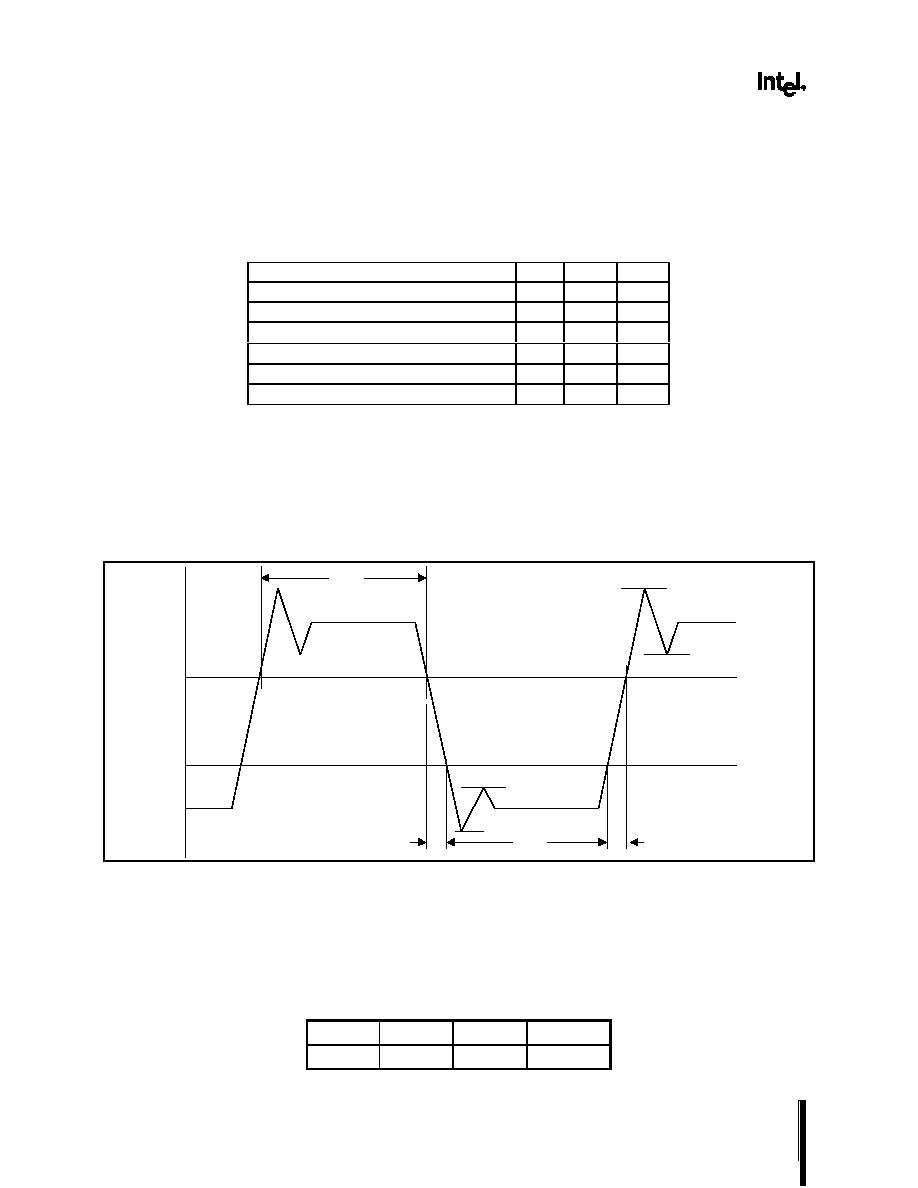
4.6.2.1
BCLK Signal Quality Specifications and
Measurement Guidelines
Table 17 describes the signal quality specifications at the
processor core for the BCLK signal. Figure 4 describes the
signal quality waveform for the BCLK at the processor core
pins.
Table 17. BCLK Signal Quality Specifications at the Processor Core
T#
Parameter
Min
Max
Unit
V1:
BCLK V
IL
2
0.7
V
V2:
BCLK V
IH
2
1.8
V
V3:
V
IN
Absolute Voltage Range
3
-0.8
3.5
V
V4:
Rising Edge Ringback
4
1.8
V
V5:
Falling Edge Ringback
4
0.7
V
BCLK rising/falling slew-rate
0.8
4
V/ns
NOTES:
1.
Unless otherwise noted, all specifications in this table apply to all Intel mobile modules.
2.
BCLK must rise and fall monotonically between VIL,BCLK and VIH, BCLK.
3.
The mobile Celeron processor PSB clock overshoot and undershoot specification for 66-megahertz operation.
4.
The rising and falling edge ringback voltage specified is the minimum (rising) or maximum (falling) absolute
voltage the BCLK signal can dip back to after passing the VIH (rising) or VIL (falling) voltage limits.
5.
For proper signal termination, refer to the Clocking Guidelines in the Mobile Pentium
Æ
II Processor / 440BX
PCIset Advanced Platform Recommend Design and Debug Practices.
V2
V1
V3
V3
T3
V5
V4
T6
T4
T5
000806
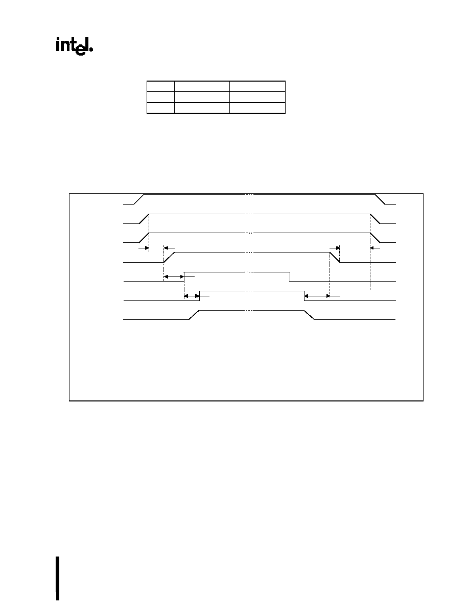
Figure 4. BCLK, TCK, PICCLK Generic Clock Waveform at the Processor Core Pin
4.7
The Voltage Regulator
The DC voltage regulator (DC/DC converter) provides the
appropriate core voltage, the I/O ring voltage, and the
sideband signal pullup voltage for the Celeron processor
mobile module. The voltage range is 5 volts-21 volts.
4.7.1
Voltage Regulator Efficiency
Table 18 lists the voltage regulator efficiencies.
Table 18. Typical Voltage Regulator Efficiency
Icore, A
3
V_DC, V
I_DC, A
2
Efficiency
1
1
5.0
0.370
82.8%

23
Celeron
TM
Processor Mobile Module MMC-1
at 466 MHz and 433 MHz
2
5.0
0.702
88.8%
3
5.0
1.044
89.8%
4
5.0
1.404
89.7%
5
5.0
1.762
88.1%
6
5.0
2.144
86.4%
7
5.0
2.528
85.0%
1
12.0
0.159
79.7%
2
12.0
0.295
87.0%
3
12.0
0.438
87.8%
4
12.0
0.584
87.3%
5
12.0
0.736
86.1%
6
12.0
0.890
84.9%
7
12.0
1.043
83.8%
1
21.0
0.091
79.3%
2
21.0
0.170
86.0%
3
21.0
0.253
87.3%
4
21.0
0.340
85.3%
5
21.0
0.429
84.1%
6
21.0
0.519
82.9%
7
21.0
0.617
80.7%
NOTES:
1.
These efficiencies will change with future voltage regulators that accommodate wider ranges of input
voltages.
2.
With V_DC applied and the voltage regulator off, typical leakage is 0.3 mA with a maximum of 0.7 mA.
3.
Icore indicates the CPU core current being drawn during test and measurement.
4.7.2.
Control of the Voltage Regulator
The VR_ON pin turns the DC voltage regulator on or off. The
VR_ON pin should be controlled as a function of the SUSB#,
which controls the system's power planes. VR_ON should
switch high only when the following conditions are met:
V_5(s) => 4.5 volts and V_DC => 4.75 volts.
Caution- Turning on VR_ON prior to meeting these
conditions will severely damage the Celeron processor
mobile module.
The VR_PWRGD signal indicates that the voltage regulator
power is operating at a stable voltage level. Use
VR_PWRGD on the system electronics to control power
inputs and to gate PWROK to the PIIX4E/M.
Table 19 lists the voltage signal definitions and sequences,
and Figure 5 shows the signal sequencing and the voltage
planes sequencing required for normal operation of the
Celeron processor mobile module MMC-1.

24
Celeron
TM
Processor Mobile Module MMC-1
at 466 MHz and 433 MHz
4.7.2.1
Voltage Signal Definition and Sequencing
Table 19. Voltage Signal Definitions and Sequences
Signal
Source
Definitions and Sequences
V_DC
System
Electronics
DC voltage is driven from the power supply and is required to be between 5V
and 21V DC. V_DC powers the module's DC-to-DC converter for processor
core and I/O voltages. It cannot be hot inserted or removed while V_DC is
powered on.
V_3
System
Electronics
V_3 is supplied by the system electronics for the 82443DX.
V_5
System
Electronics
V_5 is supplied by the system electronics for the 82443DX's 5V-reference
voltage and the voltage regulator.
V_3S
System
Electronics
V_3S is supplied by the system electronics. This is a 3.3V power supply that is
turned off during suspend during system states STR, STD and Soff.
VR_ON
System
Electronics
Enables the voltage regulator circuit. When driven active high (3.3V) the
voltage regulator circuit on the module is activated. The signal driving VR_ON
should be a digital signal with a rise/fall time of less than or equal to 1
µ
s. (VIL
(max)=0.4V, VIH (min)=3.0V).
V_CORE
(also a host bus GTL+
termination voltage VTT)
Module
A result of VR_ON being asserted, V_CORE is an output of the DC-DC
regulator on the module and is driven to the core voltage of the processor. It is
also used as the host bus GTL+ termination voltage, known as VTT.
V_BSB_IO
Module
V_BSB_IO is 1.8V. The system electronics uses this voltage to power the L2
cache-to-processor interface circuitry.
VR_PWRGD
Module
Upon sampling the voltage level of V_CORE (minus tolerances for ripple),
VR_PWRGD is driven active high. If VR_PWRGD is not sampled active within
1 second of the assertion of VR_ON, then the system electronics should
deassert VR_ON. After V_CORE is stabilized, VR_PWRGD will assert to logic
high (3.3V). This signal must not be pulled up by the system electronics.
VR_PWRGD should be "ANDed" with V_3s to generate the PIIX4E/M input
signal, PWROK. The system electronics should monitor VR_PWRGD to verify
it is asserted high prior to the active high assertion of PIIX4E/M PWROK.
V_CPUIO
Module
V_CPUIO is 2.5V. The system electronics uses this voltage to power the
PIIX4E/M-to-processor interface circuitry, as well as the HCLK(0:1) drivers for
the processor clock.
The following list provides additional specifications and clarifications of the power sequence timing and Figure 5
provides an illustration of the power sequence timing.
1. The VR_ON signal may only be asserted to a logical high by a digital signal after V_DC
4.7 volts, V_5
4.5
volts and V_3
3.0 volts.
2. The Rise Time and Fall Time of VR_ON must be less than or equal to 1 microsecond when it goes through its Vil
to Vih.
3. VR_ON has its Vil(max) = +0.4 volts and Vih(min) = +3.0 volts.
4. The VR_PWRGD will get asserted to logic high (3.3 volts) after V_CORE is stabilized and V_DC reaches 5.0
volts. This signal should not and can not be pulled up by the system electronics.
5. In the power-on process, Intel recommends to raise the higher voltage power plane first (V_DC), followed by the
lower power planes (V_5, V_3), and finally assert VR_ON after above voltage levels are met on all rails. The
power-off process should be the reverse process, i.e. VR_ON gets deasserted, followed by the lower power
planes, and finally the higher power plane.
6. VR_ON must monotonically rise through its Vil to Vih and fall through its Vih to Vil points. The sign of slope can
not change between Vil and Vih in rising and Vih and Vil in falling.
7. VR_ON must provide an instantaneous in-rush current to the module with the following values as listed in Table
20.
25
Celeron
TM
Processor Mobile Module MMC-1
at 466 MHz and 433 MHz
Table 20. VR_ON In-rush Current
Instantaneous
DC Operating
MAX
41.0 mA
0.1
µ
A
TYP
0.2 mA
0.0
µ
A
NOTE:
These values are based on a 3.3V VR_ON signal.
8. VR_ON Valid-Low Time: This specifies how long VR_ON needs to be low for a valid off before VR_ON can be
turned back on again. In going from a valid on to off and then back on, the following conditions must be met to
prevent damage to the OEM system or the Intel mobile module:
∑
VR_ON must be low for 1 millisecond.
∑
The original voltage level requirements for turn-on must be met before assertion of VR_ON (i.e. V_DC
4.7
volts, V_5
4.5 volts, and V_3
3.0 volts).
POWER SEQUENCE TIMING
V_DC
1. PWROK on I/O board should be active on when VR_PWRGD is active and V_3S is good.
2. CPU_RST from I/O board should be active for a minimum of 6 ms after PWROK is active and PLL_STP# and CPU_STP# are
inactive. Note that PLL_STP# is an AND condition of RSMRST# and SUSB# on the PIIX4E/M.
3. V_DC >= 4.7V, V_5>=4.5V, V_3S>=3.0V.
4. V_CPUPU and V_CLK are generated on the Intel Mobile Module.
5. This is the 5V power supplied to the processor module connector. This should be the first 5V plane to power up.
6. VR_PWRGD is specified to its associated high/active by the module regulator within less than or equal to 6 ms max. after the
assertion of VR_ON.
V_3
V_5
VR_PWRGD
V_3S
VR_ON
0 MS MIN
0 MS MIN
0 MS MIN
6
3
V_CPUPU/
V_CLK
5
Figure 5. Power-on Sequence Timing
4.7.3
Power Planes: Bulk Capacitance
Requirements
In order to provide adequate filtering and in-rush current
protection for any system design, bulk capacitance is
required. A small amount of bulk capacitance is supplied on
the module. However, in order to achieve proper filtering
additional capacitance should be placed on the system
electronics.
Table 21 details the bulk capacitance requirements for the
system electronics.
26
Celeron
TM
Processor Mobile Module MMC-1
at 466 MHz and 433 MHz
Table 21. Capacitance Requirements per Power Plane
Power Plane
Capacitance Requirements
ESR
Ripple Current
Rating
V_DC
100 uf, 0.1 uf, 0.01 uf
1
20 m
1-3.5A
3
20% tolerance at 35V
V_5
100 uf, 0.1 uf, 0.01 uf
1
100 m
1A
20% tolerance at 10V
V_3
470 uf, 0.1 uf, 0.01 uf
1
100 m
1A
20% tolerance at 6V
V_3S
100 uf, 0.1 uf, 0.01 uf
1
100 m
N/A
20% tolerance at 6V
V_CPUIO
2
2.2 uf, 8200 pf
1
N/A
N/A
20% tolerance at 6V
NOTES:
1.
Placement of above capacitance requirements should be located near the connector.
2.
V_CPUIO filtering should be located next to the system clock synthesizer.
3.
Ripple current specification depends on V_DC input. For 5.0V V_DC, a 3.5-A device is required.
4.
For V_DC at 18V or higher, 1A is sufficient.
4.7.4
Surge Current Guidelines
This section provides the results of a worst case, surge
current analysis. The analysis determines the maximum
amount of surge current that the Celeron processor mobile
module MMC-1 can manage.
In the analysis, the module has two 4.7 microfarads with an
ESR of 0.15 ohms total. The MMC-1 connector is
approximately 30 milliohms of series resistance, for a total
series resistance of .18 ohms. If the user powers the system
with the A/C adapter (18 volts), the amount of surge current
on the module would be approximately 100 amperes. This
information is also used to develop I/O bulk capacitance
requirements. See Table 20 for more information.
Note: Depending on the system electronics design, different
impedances may yield different result. A thorough analysis
should be performed to understand the implications of surge
current on their system.
Figure 6 shows an electrical model used when analyzing
instantaneous power-on conditions, and Figure 7 illustrates
the results with a SPICE simulation.
Figure 6. Instantaneous In-rush Current Model
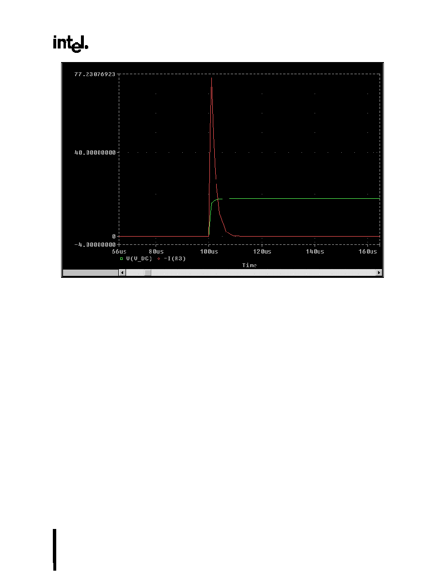
27
Celeron
TM
Processor Mobile Module MMC-1
at 466 MHz and 433 MHz
Figure 7. Instantaneous In-rush Current
Due to the stringent component height requirements of the
Celeron processor mobile module, Polymerized Organic
Semiconductor capacitors must be used as input bulk
capacitance in the voltage regulator circuit. Because of the
capacitor's susceptibility to high in-rush current, special care
must be taken. One way to soften the in-rush current and
provide overvoltage and overcurrent protection is to ramp up
V_DC slowly using a circuit similar to the one shown in
Figure 8.

28
Celeron
TM
Processor Mobile Module MMC-1
at 466 MHz and 433 MHz
NOTE:
Values shown are for reference only.
Figure 8. Overcurrent Protection Circuit
4.7.4.1
Slew-rate Control: Circuit Description
In Figure 8, PWR is the voltage generated by applying the
AC Adaptor or Battery. M1 is a low R
DS
(on) P-Channel
MOSFET such as a Siliconix* SI4435DY. When the voltage-
On PWR is applied and increased to over 4.75 volts, the
UNDER_VOLTAGE_LOCKOUT circuit allows R4 to pull up
the gate of M3 to start a turn-on sequence. M3 pulls its drain
toward ground, forcing current to flow through R2. M1 will
not start to source any current until after t_delay with t_delay
defined as:
t_delay
.
.
R2 C9 ln 1
Vt
Vpwr Vgs_max
Vgs_max
.
R16
R16 R2
Vpwr
The manufacturer's Vgs_max specification of 20 volts must
never be exceeded. However, Vgs_max must be high
enough to keep the RDS (On) of the device as low as
possible. After the initial t_delay, M1 will begin to source
current and V_DC will start to ramp up. The ramp up time,
t_ramp, is defined as:
t_ramp
.
.
R2 C9 ln 1
Vsat
Vgs_max
t_delay
Maximum current during the voltage ramping is:
I
.
Ctotal
Vpwr
t_ramp
As shown in the circuit in Figure 8: t_delay = 5.53 ms; t_tran = 14.0 ms; and I_max = 146 mA.
Figure 9 shows a SPICE simulation of the circuit in Figure 8.
To increase the reliability of the Tantalum capacitors, use a
slew-rate control circuit as described in Figure 8 and voltage
derate the capacitor about 50 percent. For example, for a
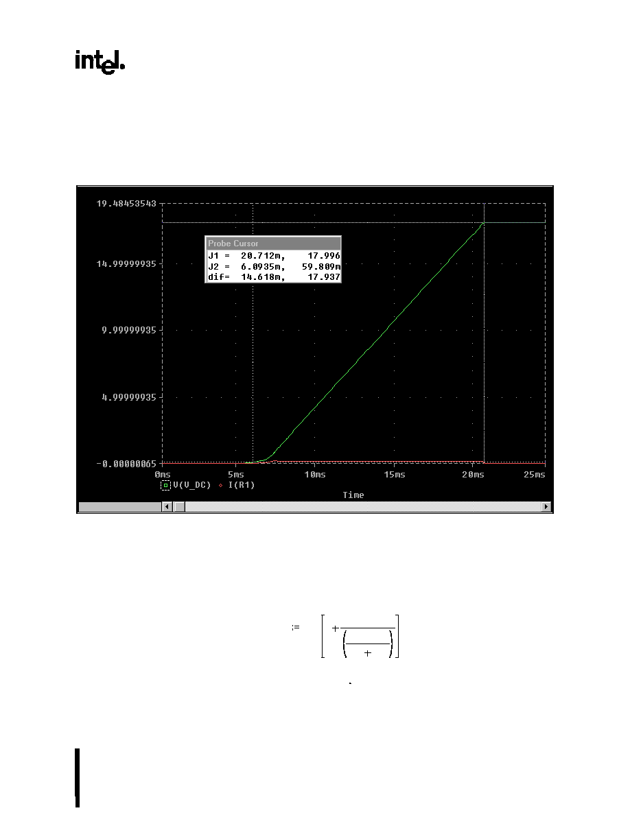
29
Celeron
TM
Processor Mobile Module MMC-1
at 466 MHz and 433 MHz
maximum input voltage of 18 volts, use a 35-volt, low ESR
capacitor with high ripple current capability. Place five, 22-
microfarad/35-volt capacitors on the baseboard directly at
the V_DC pins of the connector.
The slew-rate control circuit should also be applied to every
input power source to the system V_DC to provide the most
protection. If all power is logically "OR'ed" together at the
PWR node, there is still a potential problem. For example, if
a 3X3 Li-Ion battery pack is powering the system (12 volts at
PWR), and the AC Adaptor (18 volts) is plugged into the
system, it will immediately source current to the PWR node
and V_DC rapidly. This is because the slew-rate control is
already ON. Therefore, the slew-rate control must be applied
to every input power source to provide the most protection.
Figure 9. Spice Simulation Using In-rush Protection (Example Only)
4.7.4.2
Undervoltage Lockout: Circuit Description
(V_uv_lockout)
The circuit shown in Figure 8 provides an undervoltage
protection and locks out the applied voltage to module to
prevent an accidental turn-on at low voltage. The output of
this circuit, pin 1 of the LM339 comparator, is an open-
collector output. It is low
when the applied voltage at PWR is less than 4.75 volts.
This voltage can be calculated with the following equation
with the voltage across D7 as 2.5 volts (D7 is a 2.5-volt
reference generator).
V_uv_lockout
.
Vref 1
R17
.
R18 R25
R18 R25
=
V_uv_lockout
4.757 volts
30
Celeron
TM
Processor Mobile Module MMC-1
at 466 MHz and 433 MHz
4.7.4.3
Overvoltage Lockout: Circuit Description
(V_ov_lockout)
The Celeron processor mobile module MMC-1is specified to
operate with a maximum input voltage of 21 volts. This
circuit locks out the input voltage if it exceeds the maximum
21 volts. The output of this circuit, Pin 14 of the LM339
comparator, is an open collector output. It is low when the
applied voltage at PWR is more than 21 volts. This voltage
can be calculated with the following equation:
V_ov_lockout
.
.
Vref
R26
R26 R27
1
R24
R23
=
V_ov_lockout 20.998 volt
4.7.4.4
Overcurrent Protection: Circuit Description
Figure 8 shows that the circuit detects an overcurrent
condition and cuts off the input voltage applied to the
Celeron processor mobile module. This circuit has two
different current limit trip points. This takes into account the
different maximum current drain by the Celeron processor
mobile module at different input voltages. Assuming the AC
Adaptor voltage is 18 volts and the battery is a 3x3 Li-Ion
configuration with a minimum of 7.5 volts, the maximum
current for the above circuit can be calculated using the
following expression:
With AC Adaptor (I_wAdaptor):
I_wAdaptor
.
Vref Vbe_Q1
R14
R13
R1
I_wAdaptor = 0.989
∑
amp
Without AC Adaptor (I_woAdaptor):
I_woAdaptor
.
Vref Vbe_Q1
.
R14 R33
R14 R33
R13
R1
I_woAdaptor = 2.375
∑
amp
4.8
Active Thermal Feedback
Table 22 identifies the addresses allocated for the SMBus
thermal sensor.
Table 22. Thermal Sensor SMBus Address Table
Function
SMBus Address
Thermal Sensor
1001 110
NOTE:
The thermal sensor used is compliant with SMBus addressing. Please refer to the PentiumÆ II processor Thermal Sensor
Interface Specification.
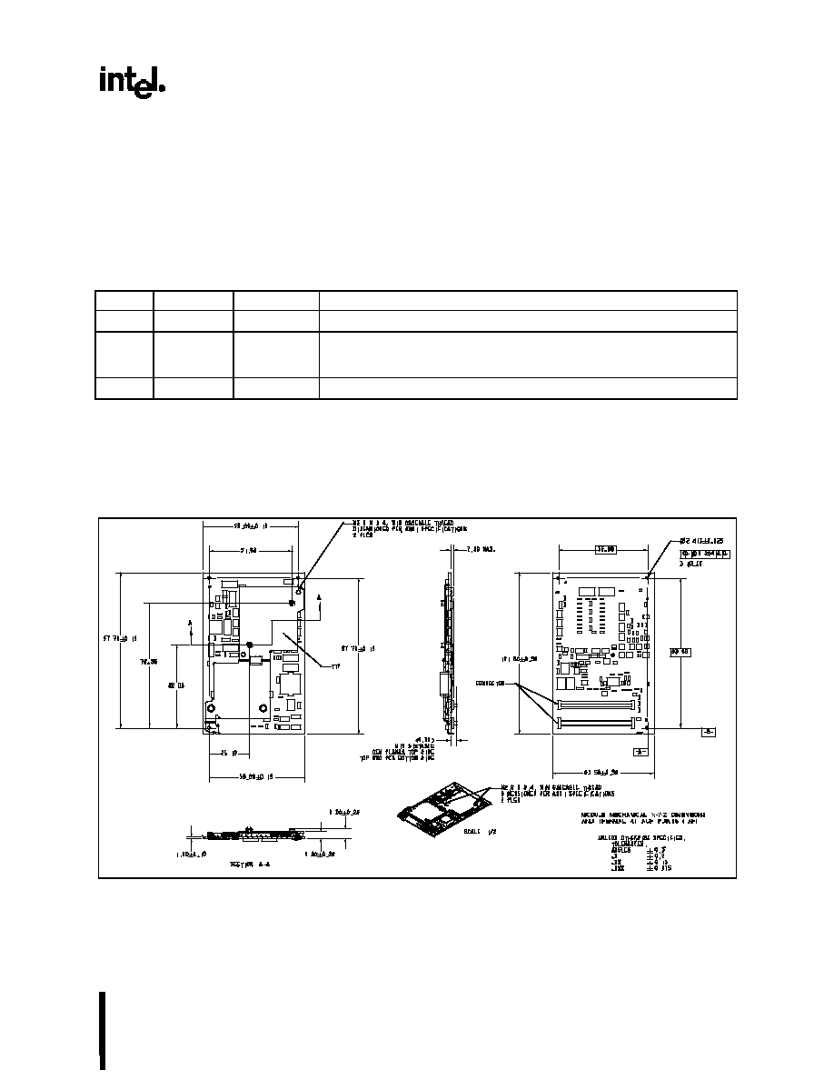
31
Celeron
TM
Processor Mobile Module MMC-1
at 466 MHz and 433 MHz
4.9
Thermal Sensor Configuration Register
The configuration register of the thermal sensor controls the
operating mode (Auto Convert vs. Standby) of the device.
Since the processor temperature varies dynamically during
normal operation, Auto Convert mode should be used
exclusively to monitor processor temperature. Table 23
shows the format of the configuration register. If the
RUN/STOP bit is low, then the thermal sensor enters auto-
conversion mode. If the RUN/STOP bit is set high, then the
thermal sensor immediately stops converting and enters
Standby mode. The thermal sensor will still perform
temperature conversions in Standby mode when it receives
a one-shot command. However, the result of a one-shot
command during Auto Convert mode is not guaranteed. Intel
does not recommend using the one-shot command to
monitor temperature when the processor is active, only Auto
Convert mode should be used. Refer to the Mobile Pentium
Æ
II Processor and Pentium
Æ
II Processor Mobile Module
Thermal Sensor Interface Specifications .
Table 23. Thermal Sensor Configuration Register
Bit
Name
Reset State
Function
7 MSB
MASK
0
Masks SMBALERT# when high.
6
RUN/STOP
0
Standby mode control bit. If low, the device enters Auto Convert mode. If high, the
device immediately stops converting, and enters standby mode where the one-
shot command can be performed.
5-0
RFU
0
Reserved for future use.
NOTE:
All RFU bits should be written as "0" and read as "don't care" for programming purposes.
5.0
MECHANICAL SPECIFICATION
This section provides the physical dimensions for the
Celeron processor mobile module MMC-1.
5.1
Module Dimensions
Figure 10 shows the board dimensions and the orientation
for the Celeron processor mobile module MMC-1.
Figure 10. Celeron Processor Mobile Module MMC-1 Board Dimensions
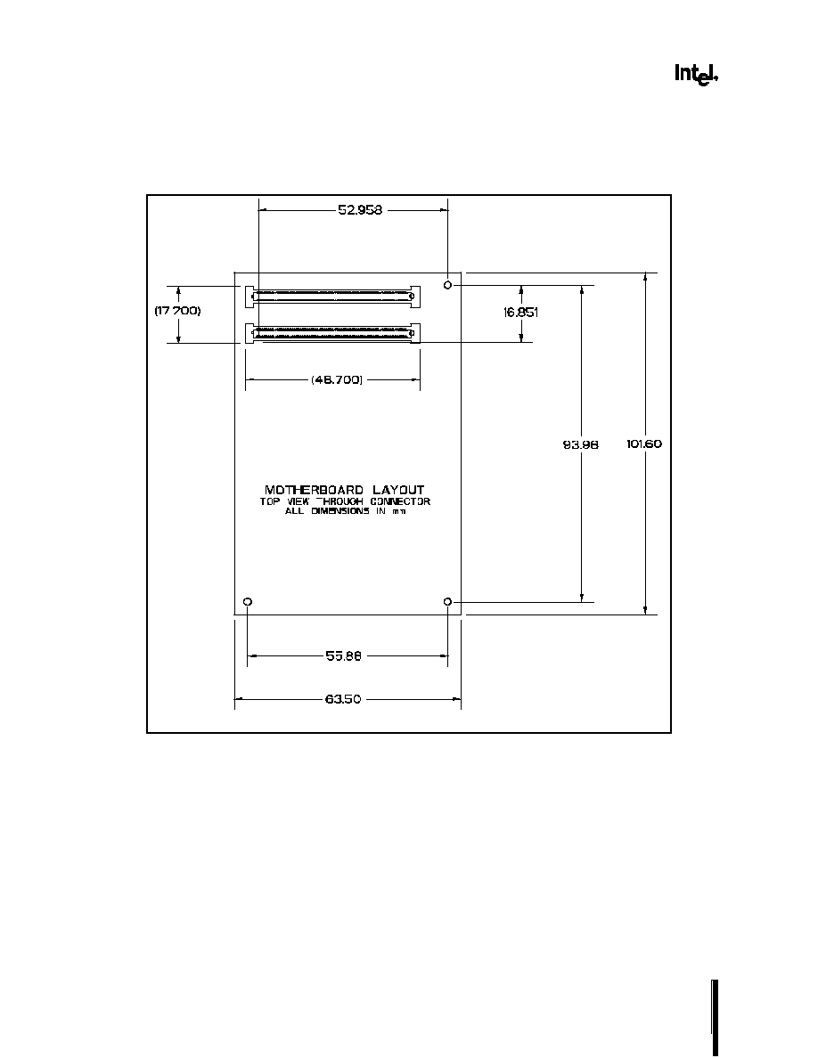
32
Celeron
TM
Processor Mobile Module MMC-1
at 466 MHz and 433 MHz
5.1.1
MMC-1 Connector Pin 1 Location
Figure 11 shows the location of pin 1 of the connector as
referenced to the adjacent mounting hole.
Figure 11. Celeron Processor Mobile Module MMC-1 Board Dimensions- Pin 1 Orientation
5.1.2
Printed Circuit Board Thickness
Figure 12 shows the minimum and maximum thickness of
the printed circuit board (PCB). The range of PCB thickness
allows for the use of different PCB technologies with current
and future Intel mobile modules.
Note: Ensure that the mechanical restraining method or
system-level EMI contacts are able to support this range of
PCB thickness for compatibility with future Intel mobile
modules.
33
Celeron
TM
Processor Mobile Module MMC-1
at 466 MHz and 433 MHz
min: 0.90 mm
max: 1.10 mm
Printed Circuit Board
Figure 12. Printed Circuit Board Thickness
5.1.3
Height Restrictions
Figure 13 shows the mechanical stack-up and the
associated component clearance requirements. This is
referred to as the module keep-out zone and should not be
entered or altered.
The system manufacturer establishes the board-to-board
clearance between the module and the system electronics
by selecting one of three possible mating connectors. The
mating connector sizes are 4 millimeters, 6 millimeters, or 8
millimeters. These three options provide the system
manufacturer with flexibility in choosing components
between the two boards. Information on these connectors
can be obtained from your local Intel representative.
NOTE:
The topside component clearance is independent of the PCB thickness.
Figure 13. Keep-out Zone
5.2
Thermal Transfer Plate
The TTP on the CPU and the 82433BX provides heat
dissipation and a thermal attach point where a system

34
Celeron
TM
Processor Mobile Module MMC-1
at 466 MHz and 433 MHz
manufacturer can attach a heat pipe, a heat spreader plate,
or a thermal solution to transfer heat through the notebook
system. See Figure 14 and Figure 15 for attachment
dimensions from the thermal interface block to the TTP.
When attaching the mating block to the TTP, a thermal
elastomer or thermal grease should be used. This material
reduces the thermal resistance. The OEM thermal interface
block should be secured with 2.0-millimeter screws using a
maximum torque of 1.5 Kg*cm to 2.0 Kg*cm (equivalent to
0.147 N*m to.197 N*m). The thread length of the 2.00-
millimeter screws should be 2.25-millimeter gageable thread
(2.25-millimeters minimum to 2.80-millimeters maximum).
The system manufacturer should use the exact dimensions
for maximum contact area to the TTP to ensure that no
warpage of the TTP occurs. If warpage occurs, the thermal
resistance of the module could be adversely affected.
The TTP thermal resistance between the processor core to
the system interface (top of the TTP) is less than 1 Celsius
per watt.
Figure 14. Thermal Transfer Plate (A)
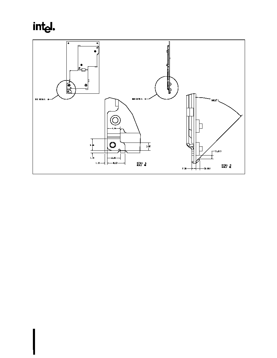
35
Celeron
TM
Processor Mobile Module MMC-1
at 466 MHz and 433 MHz
Figure 15. Thermal Transfer Plate (B)
5.3
Physical Support
5.3.1
Mounting Requirements
Three mounting holes are available for securing the module
to the system base. See Figure 11 for mounting hole
locations. These hole locations and board edge clearances
will remain fixed for all Intel mobile modules. Intel
recommends that all three mounting holes are used to
ensure long term mechanical reliability and EMI integrity of
the system.
The board edge clearance includes a 0.762 millimeters
(0.030 inches) wide EMI containment ring around the
perimeter of the module. This ring is on each layer of the
module PCB and is grounded. On the surface of the module,
the metal is exposed for EMI shielding purposes. The hole
patterns placed on the module also have a plated
surrounding ring, which can be used with a metal standoff for
EMI shielding purposes. Standoffs should be used to provide
support for the installed Celeron processor mobile module.
The distance from the bottom of the module PCB to the top
of the OEM system electronics board with the connectors
mated is 4.0 millimeters +0.16 millimeters / -0.13 millimeters.
However the warpage of the baseboard can vary and should
be calculated into the final dimensions of the standoffs used.
All calculations can be made with the Intel
Æ
MMC-1
Standoff/Receptacle Height Spreadsheet. Information on this
spreadsheet can be obtained from your local Intel
representative. Figure 16 shows the standoff support hole
patterns, the board edge clearance, the dimensions of the
EMI containment ring, and the keep-out area.
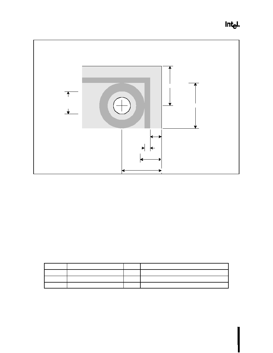
36
Celeron
TM
Processor Mobile Module MMC-1
at 466 MHz and 433 MHz
Hole detail, 3 places
0.762 mm width of EMI containment ring
1.27+/- 0.19 mm board edge to EMI ring
2.54+/-0.19 mm keep-out area
3.81+/-0.19 mm board edge to hole centerline
3.81+/-0.19 mm
4.45 mm diameter grounded ring
+ 0.050 mm
- 0.025 mm
hole diameter
2.413 mm
Figure 16. Standoff Holes, Board Edge Clearance, and EMI Containment Ring (Topside)
5.3.2
Module Weight
The Celeron processor mobile module MMC-1 weighs
approximately 50 grams.
6.0
THERMAL SPECIFICATION
6.1
Thermal Design Power
The typical TDP is the typical total power dissipation under
normal operating conditions at nominal V_CORE (CPU
power supply) while executing the worst case power
instruction mix. The power handling capability of the system
thermal solution may be reduced less than the
recommended typical thermal design power with the
implementation of firmware/software control or "throttling"
that reduces CPU power consumption and dissipation. This
includes the power dissipated by all of the relevant
components. During all operating environments, the
processor junction temperature, T
J
, must be within the range
of 0 Celsius to 100 Celsius.
6.2
Thermal Sensor Setpoint
The thermal sensor implements the SMBALERT# signal
described in the SMBus specification. SMBALERT# is
always asserted when the temperature of the processor core
thermal diode or the thermal sensor internal temperature
exceeds either the upper or lower temperature thresholds.
SMBALERT# may also be asserted if the measured
temperature equals either the upper or the lower threshold.
Table 24. Thermal Design Power Specifications
Symbol
Parameter
Typical
Notes
TDP
module
CPU Thermal Design Power
14.3
TDP
module
BX Thermal Design Power
2.3
TDP
module
Module Thermal Design Power
17.4
Module TDP = core, 82433BX, and voltage regulator
NOTE:
1. During all operating environments, the processor temperature, T
J
must be within the specified range of 0 Celsius to 100 Celsius.
2.
TDP
module
is a thermal solution design reference point for OEM thermal solution readiness for total module power.
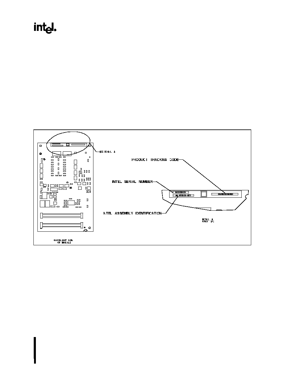
37
Celeron
TM
Processor Mobile Module MMC-1
at 466 MHz and 433 MHz
7.0
LABELING INFORMATION
The Celeron processor mobile module MMC-1 is tracked in
two ways. The first is by the Product Tracking Code (PTC).
Intel uses the PTC label to determine the assembly level of
the module. The PTC label is on the secondary side of the
module as shown in Figure 17. The PTC consists of 13
characters and contains the following information:
Example: PMH4661001AA
Definition:
AA
-
Processor Module = PM
B
-
Celeron processor mobile module MMC-1= H
CCC
-
Speed Identity = 433, 466
DD
-
Cache Size = 01 (128K)
EEE
-
Notifiable Design Revision (Start at 001)
FF
-
Notifiable Processor Revision (Start at AA)
Note: For the Celeron processor mobile module (MMC-2) the second field (B) is defined as I
Figure 17. Product Tracking Code
The second tracking method is by OEM generated software
utility. Four strapping resistors located on the Celeron
processor mobile module MMC-1determine its production
level. If connected and terminated properly, up to 16 module-
revision levels can be determined. An OEM generated
software utility can then read these ID bits with CPU IDs and
stepping IDs to provide a complete module manufacturing
revision level. For current PTC and module ID bit
information, please refer to the latest Product Change
Notification letter, which can be obtained from your local Intel
sales representative.

38
Celeron
TM
Processor Mobile Module MMC-1
at 466 MHz and 433 MHz
8.0
ENVIRONMENTAL STANDARDS
The environmental standards for the Celeron processor
mobile module MMC-1 are defined in Table 25.
Table 25. Environmental Standards
Parameter
Condition
Specification
Temperature
Non-operating
-40
∞
C to 85
∞
C
Cycle
Operating
0
∞
C to 55
∞
C
Humidity
Unbiased
85% relative humidity at 55
∞
C
Voltage
V_5
5V +/- 5%
V_3
3.3V +/- 5%
Shock
Non-operating
Half Sine, 2G, 11 msec
Unpackaged
Trapezoidal, 50G, 11 msec
Packaged
Inclined Impact at 5.7 ft/s
Packaged
Half Sine, 2 msec at 36 in. Simulated Free Fall
Vibration
Unpackaged
5 Hz to 500 Hz 2.2 gRMS random
Packaged
10 Hz to 500 Hz 1.0 gRMS
Packaged
11,800 impacts 2 Hz to 5 Hz (low frequency)
ESD Damage
Human Body Model
Non-powered test of the module only for non-
catastrophic failure. The module is tested at
2 KV and then inserted in a system for a
functional test.