Information in this document is provided solely to enable use of Intel products. Intel assumes no liability whatsoever, including infringement of any patent or
copyright, for sale and use of Intel products except as provided in Intel's Terms and Conditions of Sale for such products. Information contained herein supersedes
previously published specifications on these devices from Intel
.
© INTEL CORPORATION 1999,2000
February 2000
Order Number: 245425-001
Intel
Æ
Celeron
TM
Processor
Mobile Module: Mobile Module
Connector 2 (MMC-2) at 400 MHz,
366 MHz, 333 MHz, and 300 MHz
Datasheet
Product Features
n
Offering core frequencies of 400 MHz, 366 MHz,
333 MHz, 300 MHz
n
128K of on-die level 2 cache
n
66-MHz processor system bus speed
n
Processor core voltage regulation supports input
voltages from 5V to 21V
Above 80 percent peak efficiency
n
Integrated Active Thermal Feedback (ATF) system
ACPI Specification Rev. 1.0 compliant
Internal A/D ≠ digital signaling (SMBus) across
the module interface
Programmable trip point interrupt or poll mode
for temperature reading
n
Supports a single AGP 66-MHz, 3.3V device
n
Thermal transfer plate on the CPU and the Intel
Æ
82433BX for heat dissipation
n
Intel 82433BX Host Bridge system controller
DRAM controller supports EDO and SDRAM at
3.3V
Supports PCI CLKRUN# protocol
SDRAM clock support and self-refresh of EDO
or SDRAM during Suspend mode
3.3V only PCI bus control, Rev 2.1 compliant

Intel
Æ
Celeron
TM
Processor Mobile Module MMC-2
at 400 MHz, 366 MHz, 333 MHz, and 300 MHz
2
Information in this document is provided in connection with Intel products. No license, express or implied, by estoppel or otherwise, to any intellectual
property rights is granted by this document. Except as provided in Intel's Terms and Conditions of Sale for such products, Intel assumes no liability
whatsoever, and Intel disclaims any express or implied warranty, relating to sale and/or use of Intel products including liability or warranties relating to
fitness for a particular purpose, merchantability, or infringement of any patent, copyright or other intellectual property right. Intel products are not
intended for use in medical, life-saving, or life-sustaining applications. Intel may make changes to specifications and product descriptions at any time,
without notice.
Designers must not rely on the absence or characteristics of any features or instructions marked "reserved" or "undefined." Intel reserves these for
future definition and shall have no responsibility whatsoever for conflicts or incompatibilities arising from future changes to them.
The Celeron processor mobile modules may contain design defects or errors known as errata. Current characterized errata are available on request.
Contact your local Intel sales office or your distributor to obtain the latest specifications and before placing your product order.
Copies of documents which have an ordering number and are referenced in this document, or other Intel literature, may be obtained by calling 1-800-
548-4725 or by visiting Intel's web site at
http://www.intel.com
Copyright © Intel Corporation1999, 2000.
*Third-party brands and names are the property of their respective owners.

Intel
Æ
Celeron
TM
Processor Mobile Module MMC-2
at 400 MHz, 366 MHz, 333 MHz, and 300 MHz
3
CONTENTS
1.0
INTRODUCTION...................................................5
1.1 Revision History....................................................5
2.0
ARCHITECTURE OVERVIEW ..............................5
3.0
CONNECTOR INTERFACE..................................7
3.1 Signal Definitions...................................................7
3.1.1
Signal List...................................................8
3.1.2
Memory (109 Signals).................................9
3.1.3
AGP (60 Signals)......................................10
3.1.4
PCI (58 Signals)........................................11
3.1.5
Geyserville (4 Signals)..............................12
3.1.6
Processor/PIIX4E/M Sideband (8 Signals)13
3.1.7
Power Management (7 Signals)................14
3.1.8
Clock (9 Signals).......................................15
3.1.9
Voltages (54 Signals)................................16
3.1.10
ITP/JTAG (9 Signals)................................17
3.1.11
Miscellaneous (82 Signals).......................17
3.2 Connector Pin Assignments ..................................18
3.3 Pin and Pad Assignments .....................................21
4.0
FUNCTIONAL DESCRIPTION..............................22
4.1 Celeron Processor Mobile Module MMC-2............22
4.2 L2 Cache...............................................................22
4.3 The 82433BX Host Bridge System Controller .......22
4.3.1
Memory Organization ...............................22
4.3.2
Reset Strap Options .................................23
4.3.3
PCI Interface.............................................23
4.3.4
AGP Interface...........................................23
4.4 Power Management ..............................................23
4.4.1
Clock Control Architecture........................23
4.4.2
Normal State .............................................25
4.4.3
Auto Halt State..........................................25
4.4.4
Stop Grant State.......................................25
4.4.5
Quick Start State.......................................25
4.4.6
HALT/Grant Snoop State..........................25
4.4.7
Sleep State ...............................................25
4.4.8
Deep Sleep State......................................26
4.5 Typical POS/STR Power .......................................26
4.6 Electrical Requirements ........................................27
4.6.1
DC Requirements .....................................27
4.6.2
AC Requirements......................................28
4.6.2.1
PSB Clock Signal Quality Specifications
and Measurement Guidelines .............29
4.7 Voltage Regulator..................................................29
4.7.1
Voltage Regulator Efficiency.....................29
4.7.2
Control of the Voltage Regulator...............30
4.7.2.1
Voltage Signal Definition and
Sequencing.........................................31
4.7.3
Power Planes: Bulk Capacitance
Requirements ...........................................................32
4.7.4
Surge Current Guidelines .........................34
4.7.4.1
Slew-rate Control: Circuit Description .36
4.7.4.2
Undervoltage Lockout: Circuit
Description (V_uv_lockout).................37
4.7.4.3
Overvoltage Lockout: Circuit Description
(V_ov_lockout)....................................37
4.7.4.4
Overcurrent Protection: Circuit
Description..........................................38
4.8 Active Thermal Feedback......................................39
4.9 Thermal Sensor Configuration Register................39
5.0
MECHANICAL SPECIFICATION...........................39
5.1 Module Dimensions...............................................39
5.1.2
Pin 1 Location of the MMC-2 Connector...41
5.1.3
Printed Circuit Board Thickness................41
5.1.4
Height Restrictions ...................................42
5.2 Thermal Transfer Plate..........................................42
5.3 Module Physical Support ......................................44
5.3.1
Module Mounting Requirements ...............44
5.3.2
Module Weight ..........................................45
6.0
THERMAL SPECIFICATION.................................45
6.1 Thermal Design Power .........................................45
6.2 Thermal Sensor Setpoint.......................................45
7.0
LABELING INFORMATION...................................46
8.0
ENVIRONMENTAL STANDARDS.........................47

Intel
Æ
Celeron
TM
Processor Mobile Module MMC-2
at 400 MHz, 366 MHz, 333 MHz, and 300 MHz
4
FIGURES
Figure 1. Block Diagram of the Celeron Processor
Mobile Module MMC-2...........................................6
Figure 2. 400-Pin Connector Footprint Pad Numbers.........21
Figure 3. Clock Control States ............................................24
Figure 4. BCLK, TCK, and PICCLK Generic Clock Waveform
at the Processor Core Pins ...................................29
Figure 5. Power-on Sequence Timing.................................32
Figure 6. Instantaneous In-rush Current Model...................34
Figure 7. Instantaneous In-rush Current.............................35
Figure 8. Overcurrent Protection Circuit..............................36
Figure 9. Spice Simulation Using In-rush Protection
(Example ONLY))................................................37
Figure 10. Board Dimensions with 400-Pin Connector
Orientation .........................................................40
Figure 11. Board Dimensions with 400-Pin Connector- Pin 1
Orientation .........................................................41
Figure 12. Printed Circuit Board Thickness.........................41
Figure 13. Keep-out Zone...................................................42
Figure 14. Thermal Transfer Plate (A) ................................43
Figure 15. Thermal Transfer Plate (B) ................................44
Figure 16. Standoff Holes, Board Edge Clearance, and EMI
Containment Ring ..............................................45
Figure 17. Product Tracking Information.............................46
TABLES
Table 1. Connector Signal Summary ....................................7
Table 2. Memory Signal Descriptions ...................................9
Table 3. AGP Signal Descriptions.......................................10
Table 4. PCI Signal Descriptions ........................................11
Table 5. Geyserville Descriptions .......................................12
Table 6. Processor/PIIX4E/M Sideband Signal
Descriptions..........................................................13
Table 7. Power Management Signal Descriptions ..............14
Table 8. Clock Signal Descriptions .....................................15
Table 9. Voltage Descriptions .............................................16
Table 10. ITP/JTAG Pins ....................................................17
Table 11. Miscellaneous Pins .............................................17
Table 12. Connector Pin Assignments................................18
Table 13. Connector Specifications ....................................22
Table 14. Configuration Straps for the 82433BX Host Bridge
System Controller ...............................................23
Table 15. Clock State Characteristics.................................26
Table 16. POS/STR Power.................................................26
Table 17. Power Supply Design Specifications ...................27
Table 18. AC Specifications at the Processor Core Pins ....28
Table 19. BCLK Signal Quality Specifications at the
Processor Core...................................................29
Table 20. Typical Voltage Regulator Efficiency...................30
Table 21. Voltage Signal Definitions and Sequences .........31
Table 22. VR_ON In-rush Current ......................................32
Table 23. Capacitance Requirement per Power Plane........33
Table 24. Thermal Sensor SMBus Address Table..............39
Table 25. Thermal Sensor Configuration Register ..............39
Table 26. Thermal Design Power Specification ..................45
Table 27. Environmental Standards....................................47

Intel
Æ
Celeron
TM
Processor Mobile Module MMC-2
at 400 MHz, 366 MHz, 333 MHz, and 300 MHz
5
1.0
INTRODUCTION
This document provides the technical information for
integrating the Celeron processor mobile module Connector
2 (MMC-2) into the latest notebook systems for today's
notebook market.
Building around this design gives the system manufacturer
these advantages:
∑
Avoids complexities associated with designing high-
speed processor core logic boards.
∑
Provides an upgrade path from previous Intel
Æ
Mobile
Modules using a standard interface.
1.1
Revision History
Date
Revision
Updates
3/1999
1.0
Initial release.
5/1999
2.0
ß
New 333-MHz processor
speed
ß
POS/STR corrections
ß
ESD clarification
ß
VR_ON and VR_PWRGD
correction
ß
L2 cache correction
ß
Power sequence
clarification
6/1999
3.0
New 400-MHz processor
speed
2/2000
4.0
Updated Table 24
2.0
ARCHITECTURE OVERVIEW
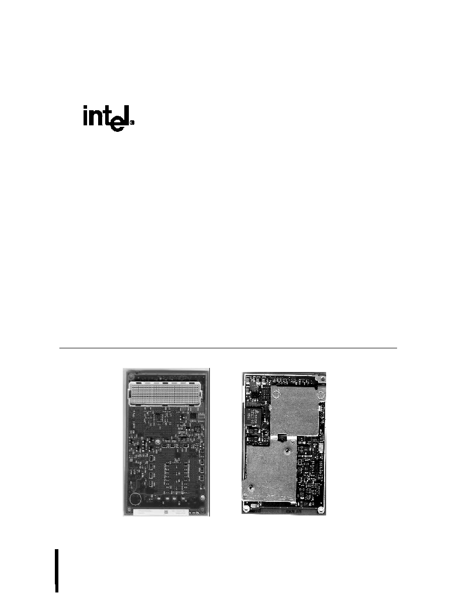
A highly integrated assembly, the Celeron processor mobile
module MMC-2 contains the mobile Celeron processor core
and its immediate system-level support. The Celeron
processor mobile module MMC-2 offers core speeds of 400
megahertz, 366 megahertz, 333 megahertz, and 300
megahertz. All processor speeds have a 66-megahertz
processor system bus speed (PSB).
The PIIX4E/M PCI/ISA Bridge is one of two large-scale
integrated devices of the Intel 440BX AGPset. A notebook's
system electronics must include a PIIX4E/M device to
connect to the Celeron processor mobile module MMC-2.
The PIIX4E/M provides extensive power management
capabilities and supports the Intel
Æ
82433BX Host Bridge,
the second integrated device. Key features of the 82433BX
Host Bridge include the DRAM controller, which supports
EDO at 3.3 volts with a burst read at 7-2-2-2 (60
nanoseconds) or SDRAM at 3.3 volts with a burst read at 8-
1-1-1 (66 megahertz, CL=2). The 82433BX Host Bridge also
provides a PCI CLKRUN# signal to request PIIX4E/M to
regulate the PCI clock on the PCI bus. The 82433BX clock
enables Self Refresh mode of EDO or SDRAM during
Suspend mode and is compatible with SMRAM (C_SMRAM)
and Extended SMRAM (E_SMRAM) modes of power
management. E_SMRAM mode supports write-back
cacheable SMRAM up to 1 megabyte.
A thermal transfer plate (TTP) on the 82433BX Host Bridge
and the CPU provides heat dissipation and a thermal attach
point for the system manufacturer's thermal solution.
An on-board voltage regulator converts the system DC
voltage to the processor's core and I/O voltage. Isolating the
processor voltage requirements allows the system
manufacturer to incorporate different processor variants into
a single notebook system.
Supporting input voltages from 5 volts to 21 volts, the
processor core voltage regulation enables an above 80
percent peak efficiency and decouples processor voltage
requirements from the system.
The Celeron processor mobile module MMC-2 also
incorporates Active Thermal Feedback (ATF) sensing,
compliant to the ACPI Specification Rev 1.0. A system
management bus (SMBus) supports the internal and external
temperature sensing with programmable trip points.