Other brands and names are the property of their respective owners
Information in this document is provided in connection with Intel products Intel assumes no liability whatsoever including infringement of any patent or
copyright for sale and use of Intel products except as provided in Intel's Terms and Conditions of Sale for such products Intel retains the right to make
changes to these specifications at any time without notice Microcomputer Products may have minor variations to this specification known as errata
January 1994
COPYRIGHT
INTEL CORPORATION 1995
Order Number 241267-003
Intel386
TM
DX MICROPROCESSOR
32-BIT CHMOS MICROPROCESSOR WITH
INTEGRATED MEMORY MANAGEMENT
(PQFP SUPPLEMENT)
Y
Flexible 32-Bit Microprocessor
8 16 32-Bit Data Types
8 General Purpose 32-Bit Registers
Y
Very Large Address Space
4 Gigabyte Physical
64 Terabyte Virtual
4 Gigabyte Maximum Segment Size
Y
Integrated Memory Management Unit
Virtual Memory Support
Optional On-Chip Paging
4 Levels of Protection
Fully Compatible with 80286
Y
Object Code Compatible with All 8086
Family Microprocessors
Y
Virtual 8086 Mode Allows Running of
8086 Software in a Protected and
Paged System
Y
Hardware Debugging Support
Y
Optimized for System Performance
Pipelined Instruction Execution
On-Chip Address Translation Caches
20 25 and 33 MHz Clock
40 50 and 66 Megabytes Sec Bus
Bandwidth
Y
Numerics Support via Intel387
TM
DX
Math Coprocessor
Y
Complete System Development
Support
Software C PL M Assembler
System Generation Tools
Debuggers PSCOPE ICE
TM
-386
Y
High Speed CHMOS IV Technology
Y
132 Pin PQFP Package
(See Packaging Specification Order
231369)
The Intel386 DX Microprocessor is an entry-level 32-bit microprocessor designed for single-user applications
and operating systems such as MS-DOS and Windows The 32-bit registers and data paths support 32-bit
addresses and data types The processor addresses up to four gigabytes of physical memory and 64 terabytes
(2
46) of virtual memory The integrated memory management and protection architecture includes address
translation registers multitasking hardware and a protection mechanism to support operating systems Instruc-
tion pipelining on-chip address translation ensure short average instruction execution times and maximum
system throughput
The Intel386 DX CPU offers new testability and debugging features Testability features include a self-test and
direct access to the page translation cache Four new breakpoint registers provide breakpoint traps on code
execution or data accesses for powerful debugging of even ROM-based systems
Object-code compatibility with all 8086 family members (8086 8088 80186 80188 80286) means the
Intel386 DX offers immediate access to the world's largest microprocessor software base
241267 ≠ 1
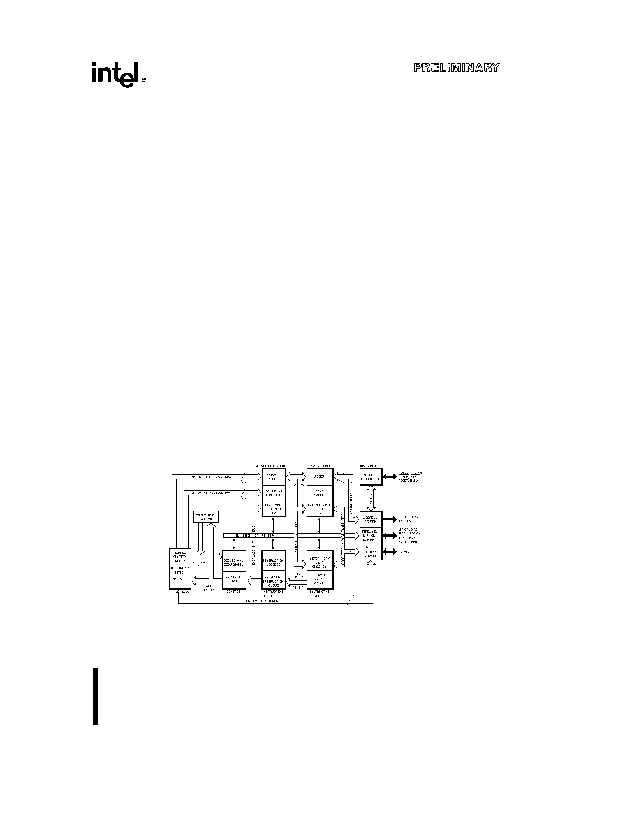
Intel386
TM
DX Pipelined 32-Bit Microarchitecture
Intel386
TM
DX and Intel387
TM
DX are Trademarks of Intel Corporation
MS-DOS and Windows are Trademarks of MICROSOFT Corporation

Intel386
TM
DX Microprocessor High-Performance 32-Bit
CHMOS Microprocessor with Integrated Memory
Management (PQFP Supplement)
CONTENTS
PAGE
1 0 PIN ASSIGNMENT
3
1 1 Pin Description Table
5
1 2 Float Pin Description
7
2 0 MECHANICAL DATA
8
2 1 Package Physical Dimensions
8
2 2 Package Thermal Specifications
11
CONTENTS
PAGE
3 0 D C A C SPECIFICATIONS
12
3 1 D C Specifications
12
3 2 A C Specifications
13
3 2 1 A C Spec Definitions
13
3 2 2 A C Specification Tables
14
3 2 3 A C Test Loads
20
3 2 4 A C Timing Waveforms
20
3 2 5 Typical Output Valid Delays
22
3 2 6 Typical Output Valid Delays
22
3 2 7 Typical Output Valid Delays
23
3 2 8 Typical Output Rise Times
23
2
Intel386
TM
DX PQFP MICROPROCESSOR
This document should be used in conjunction
with the Intel386
TM
DX Microprocessor data
sheet (order number 231630-011 October 1993)
1 0
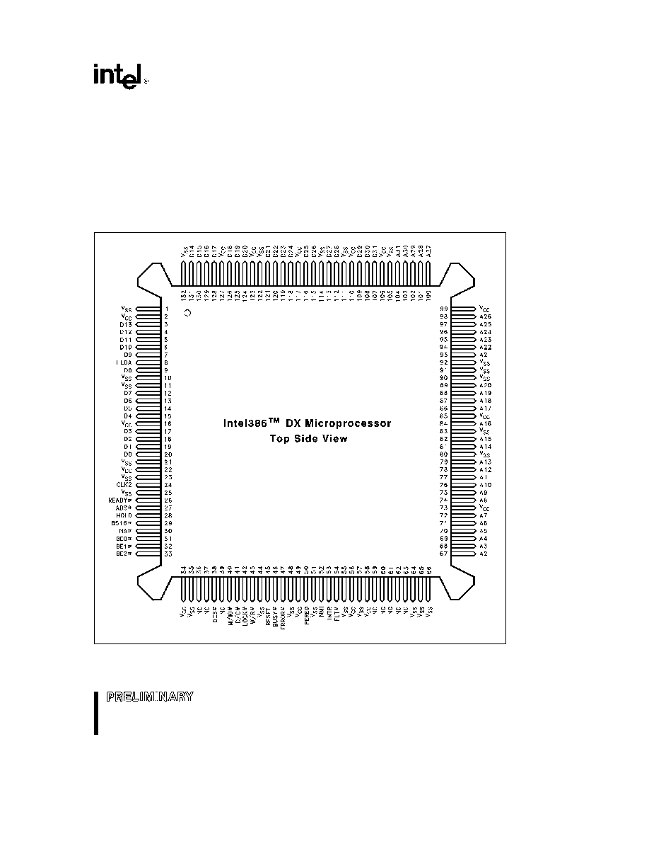
PIN ASSIGNMENT
The Intel386 DX pinout as viewed from the top side
of the component is shown by Figure 1-1
V
CC
and GND connections must be made to multi-
ple V
CC
and V
SS
(GND) pins Each V
CC
and V
SS
must be connected to the appropriate voltage level
The circuit board should include V
CC
and GND
planes for power distribution and all V
CC
and V
SS
pins must be connected to the appropriate plane
NOTE
Pins identified as ``N C '' should remain completely
unconnected
241267 ≠ 2
Figure 1-1 Intel386
TM
DX PQFP Pinout
View from Top Side
3
Intel386
TM
DX PQFP MICROPROCESSOR
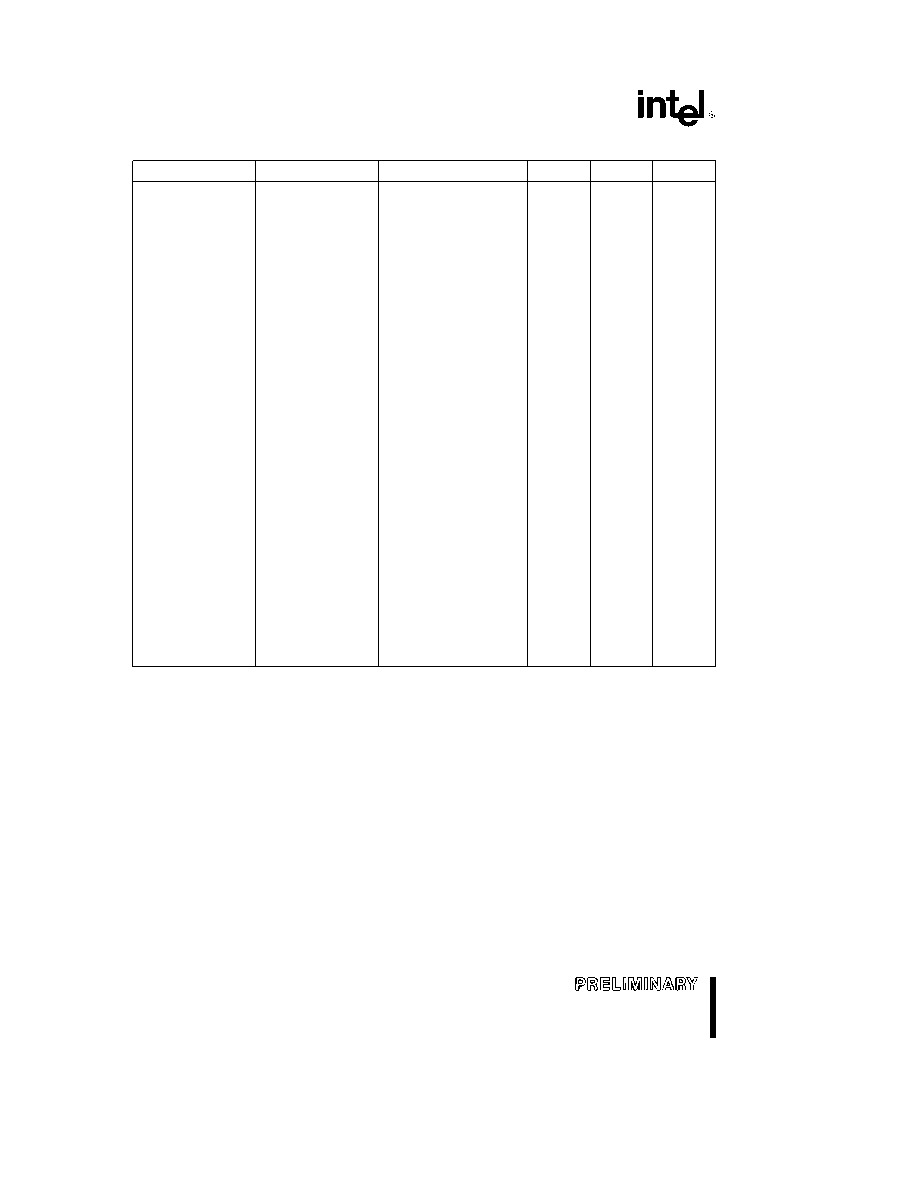
Table 1-1 Intel386
TM
DX PQFP Pinout
Functional Grouping
Address
Data
Control
N C
V
SS
V
CC
A2
67
D0
20
ADS
27
36
1
2
A3
68
D1
19
BE0
31
37
10
16
A4
69
D2
18
BE1
32
39
11
22
A5
70
D3
17
BE2
33
59
21
34
A6
71
D4
15
BE3
38
60
23
49
A7
72
D5
14
BS16
29
61
25
56
A8
74
D6
13
BUSY
46
62
35
58
A9
75
D7
12
CLK2
24
63
44
73
A10
76
D8
9
D C
41
48
85
A11
77
D9
7
ERROR
47
51
99
A12
78
D10
6
FLT
54
55
106
A13
79
D11
5
HLDA
8
57
110
A14
81
D12
4
HOLD
28
64
117
A15
82
D13
3
INTR
53
65
123
A16
84
D14
131
LOCK
42
66
127
A17
86
D15
130
M IO
40
80
A18
87
D16
129
NA
30
83
A19
88
D17
128
NMI
52
90
A20
89
D18
126
PEREQ
50
91
A21
93
D19
125
READY
26
92
A22
94
D20
124
RESET
45
105
A23
95
D21
121
W R
43
111
A24
96
D22
120
114
A25
97
D23
119
122
A26
98
D24
118
132
A27
100
D25
116
A28
101
D26
115
A29
102
D27
113
A30
103
D28
112
A31
104
D29
109
D30
108
D31
107
4
Intel386
TM
DX PQFP MICROPROCESSOR
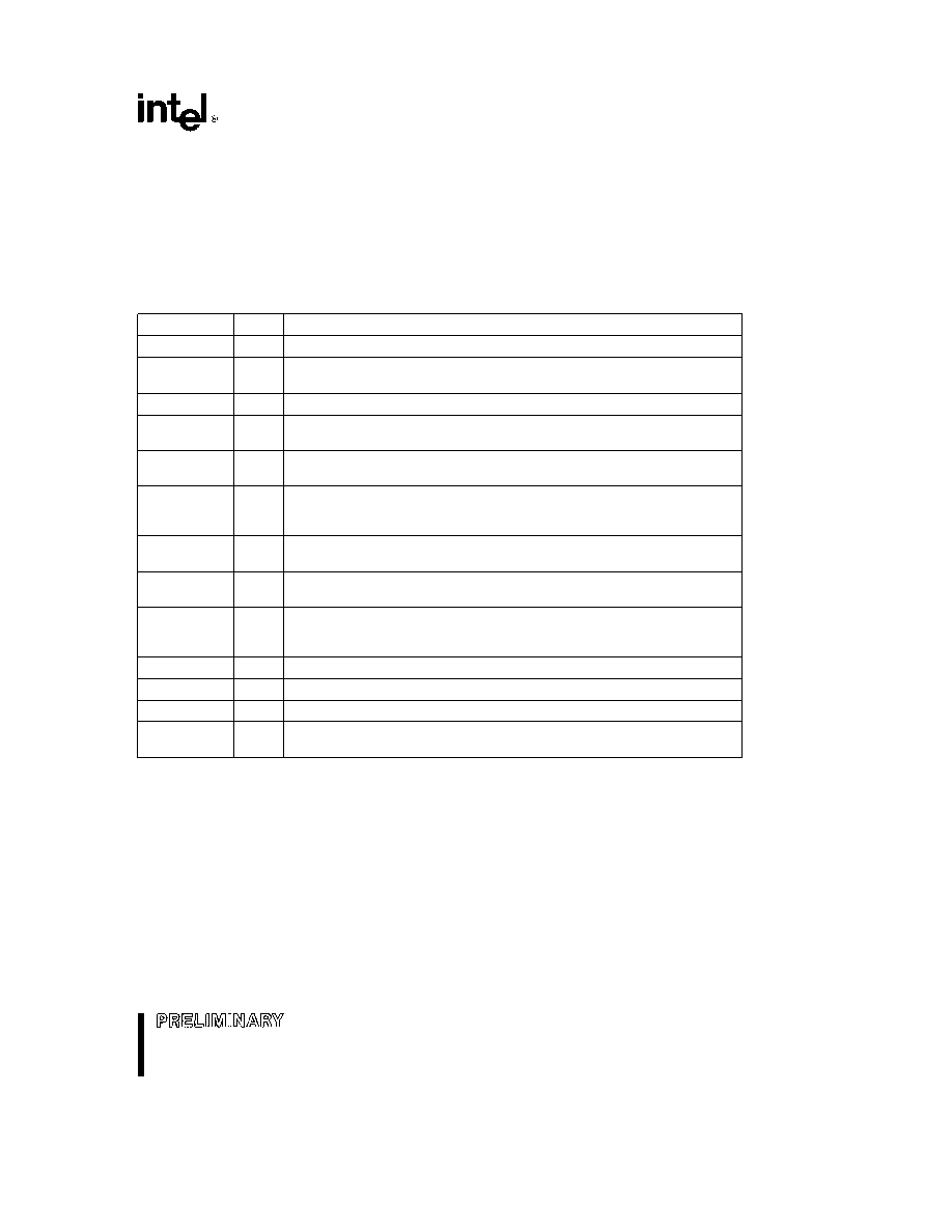
1 1 Pin Description Table
The following table lists a brief description of each pin on the Intel386 DX The following definitions are used in
these descriptions
The named signal is active LOW
I
Input signal
O
Output signal
I O
Input and Output signal
No electrical connection
Symbol
Type
Name and Function
CLK2
I
CLK2
provides the fundamental timing for the Intel386 DX
D
31
≠ D
0
I O
DATA BUS
inputs data during memory I O and interrupt acknowledge read
cycles and outputs data during memory and I O write cycles
A
31
≠ A
2
O
ADDRESS BUS
outputs physical memory or port I O addresses
BE0
≠ BE3
O
BYTE ENABLES
indicate which data bytes of the data bus take part in a bus
cycle
W R
O
WRITE READ
is a bus cycle definition pin that distinguishes write cycles from
read cycles
D C
O
DATA CONTROL
is a bus cycle definition pin that distinguishes data cycles
either memory or I O from control cycles which are interrupt acknowledge
halt and instruction fetching
M IO
O
MEMORY I O
is a bus cycle definition pin that distinguishes memory cycles
from input output cycles
LOCK
O
BUS LOCK
is a bus cycle definition pin that indicates that other system bus
masters are denied access to the system bus while it is active
ADS
O
ADDRESS STATUS
indicates that a valid bus cycle definition and address
(W R
D C
M IO
BE0
BE1
BE2
BE3
and A
31
≠ A
2
) are being
driven at the Intel386 DX pins
NA
I
NEXT ADDRESS
is used to request address pipelining
READY
I
BUS READY
terminates the bus cycle
BS16
I
BUS SIZE 16
input allows direct connection of 32-bit and 16-bit data buses
HOLD
I
BUS HOLD REQUEST
input allows another bus master to request control of the
local bus
5