© INTEL CORPORATION, 1997
December 1997
Order Number: 272755-002
EMBEDDED ULTRA-LOW POWER Intel486
TM
GX PROCESSOR
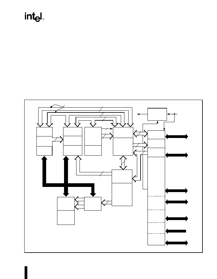
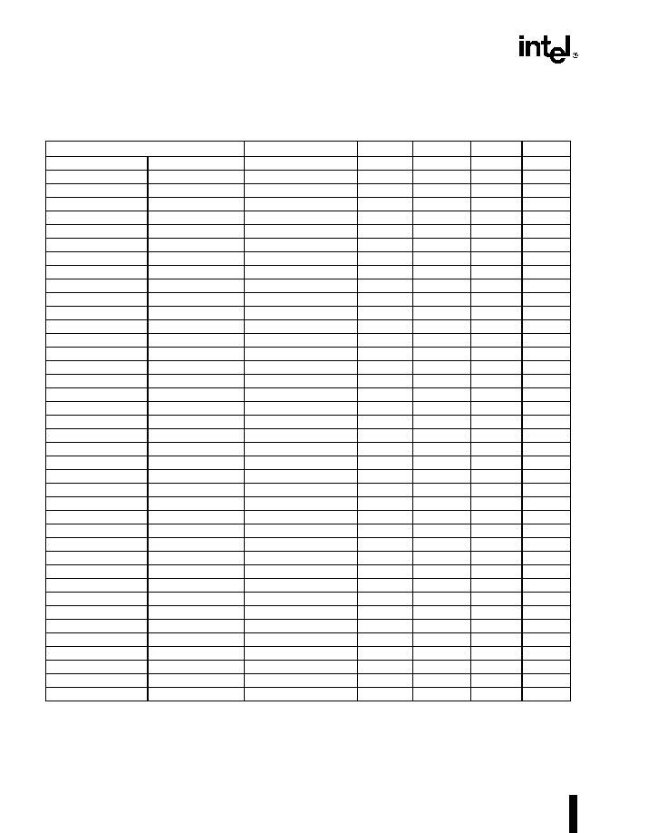
Figure 1. Embedded Ultra-Low Power Intel486TM GX Processor Block Diagram
s
Ultra-Low Power Member of the Intel486TM
Processor Family
-- 32-Bit RISC Technology Core
-- 8-Kbyte Write-Through Cache
-- Four Internal Write Buffers
-- Burst Bus Cycles
-- Data Bus Parity Generation and
Checking
-- Intel System Management Mode (SMM)
-- Boundary Scan (JTAG)
s
16-Bit External Data Bus
s
176-Lead Thin Quad Flat Pack (TQFP)
s
Separate Voltage Supply for Core Circuitry
s
Fast Core-Clock Restart
s
Auto Clock Freeze
s
Ideal for Embedded Battery-Operated and
Hand-Held Applications
A5851-01
Paging
Unit
Prefetcher
32-Byte Code
Queue
2x16 Bytes
Code
Stream
Barrel
Shifter
Cache Unit
Burst Bus
Control
Bus Control
Write Buffers
4 x 32
64-Bit Interunit Transfer Bus
Register
File
ALU
Segmentation
Unit
Descriptor
Registers
Limit and
Attribute PLA
Base/
Index
Bus
Translation
Lookaside
Buffer
8 Kbyte
Cache
Clock
Control
Control &
Protection
Test Unit
Control
ROM
Address
Drivers
CLK Input
Core
Clock
Data Bus
Transceivers
Request
Sequencer
Cache
Control
Parity
Generation
and Control
Boundary
Scan
Control
Bus Interface
D15-D0
A31-A2
BE3#- BE0#
ADS# W/R# D/C# M/IO#
PCD PWT RDY# LOCK#
PLOCK# BOFF# A20M#
BREQ HOLD HLDA
RESET SRESET INTR
NMI SMI# SMIACT#
STPCLK#
BRDY# BLAST#
KEN# FLUSH#
AHOLD EADS#
DP1-DP0, PCHK#
TCK TMS
TDI TD0
Instruction
Decode
Decoded
Instruction
Path
PCD
PWT
2
Physical
Address
32-Bit Data Bus
32-Bit Data Bus
Linear Address
Micro-
Instruction
Displacement Bus
32
32
32
32
32
128
32
32
32
20
24

Information in this document is provided in connection with Intel products. No license, express or implied, by
estoppel or otherwise, to any intellectual property rights is granted by this document. Except as provided in
Intel's Terms and Conditions of Sale for such products, Intel assumes no liability whatsoever, and Intel
disclaims any express or implied warranty, relating to sale and/or use of Intel products including liability or
warranties relating to fitness for a particular purpose, merchantability, or infringement of any patent, copyright
or other intellectual property right. Intel products are not intended for use in medical, life saving, or life
sustaining applications.
Intel may make changes to specifications and product descriptions at any time, without notice.
Designers must not rely on the absence or characteristics of any features or instructions marked "reserved" or
"undefined." Intel reserves these for future definition and shall have no responsibility whatsoever for conflicts or
incompatibilities arising from future changes to them.
The Embedded Ultra-Low Power Intel486TM GX processor may contain design defects or errors known as
errata which may cause the product to deviate from published specifications. Current characterized errata are
available on request.
Contact your local Intel sales office or your distributor to obtain the latest specifications and before placing your
product order.
Copies of documents which have an ordering number and are referenced in this document, or other Intel
literature may be obtained by calling 1-800-548-4725 or by visiting Intel's website at http://www.intel.com.
Copyright © Intel Corporation, 1997
*Third-party brands and names are the property of their respective owners.

Contents
iii
Embedded Ultra-Low Power Intel486
TM
GX Processor
1.0 INTRODUCTION ........................................................................................................................................ 1
1.1 Features ............................................................................................................................................. 1
1.2 Family Members ................................................................................................................................. 3
2.0 HOW TO USE THIS DOCUMENT ............................................................................................................. 3
3.0 PIN DESCRIPTIONS ................................................................................................................................. 3
3.1 Pin Assignments ................................................................................................................................. 3
3.2 Pin Quick Reference ........................................................................................................................... 7
4.0 ARCHITECTURAL AND FUNCTIONAL OVERVIEW ............................................................................. 15
4.1 Separate Supply Voltages ................................................................................................................ 15
4.2 Fast Clock Restart ............................................................................................................................ 16
4.3 Level-Keeper Circuits ....................................................................................................................... 17
4.4 Low-Power Features ........................................................................................................................ 18
4.4.1 Auto Clock Freeze ................................................................................................................. 18
4.5 Bus Interface and Operation ............................................................................................................. 19
4.5.1 16-Bit Data Bus ...................................................................................................................... 19
4.5.2 Parity ...................................................................................................................................... 19
4.5.3 Data Transfer Mechanism ...................................................................................................... 19
4.6 CPUID Instruction ............................................................................................................................. 27
4.6.1 Operation of the CPUID Instruction ....................................................................................... 27
4.7 Identification After Reset .................................................................................................................. 29
4.8 Boundary Scan (JTAG) .................................................................................................................... 29
4.8.1 Device Identification ............................................................................................................... 29
4.8.2 Boundary Scan Register Bits and Bit Order ........................................................................... 29
5.0 ELECTRICAL SPECIFICATIONS ........................................................................................................... 30
5.1 Maximum Ratings ............................................................................................................................. 30
5.2 DC Specifications ............................................................................................................................. 30
5.3 AC Specifications ............................................................................................................................. 34
5.4 Capacitive Derating Curves .............................................................................................................. 41
6.0 MECHANICAL DATA .............................................................................................................................. 42
6.1 Package Dimensions ........................................................................................................................ 42
6.2 Package Thermal Specifications ...................................................................................................... 43
FIGURES
Figure 1.
Embedded Ultra-Low Power Intel486TM GX Processor Block Diagram ...................................... i
Figure 2.
Package Diagram for 176-Lead TQFP Package Embedded ULP Intel486TM GX Processor .... 4
Figure 3.
Example of Supply Voltage Power Sequence ......................................................................... 16
Figure 4.
Stop Clock State Diagram with Typical Power Consumption Values ...................................... 17
Figure 5.
Logic to Generate A1, BHE# and BLE# ................................................................................... 19

Contents
iv
Figure 6.
Address Prediction for Burst Transfers (1 of 3) ........................................................................ 25
Figure 7.
Address Prediction for Burst Transfers (2 of 3) ........................................................................ 26
Figure 8.
Address Prediction for Burst Transfers (3 of 3) ........................................................................ 27
Figure 9.
CLK Waveform ......................................................................................................................... 37
Figure 10.
Input Setup and Hold Timing ................................................................................................... 37
Figure 11.
Input Setup and Hold Timing ................................................................................................... 38
Figure 12.
Output Valid Delay Timing ....................................................................................................... 38
Figure 13.
PCHK# Valid Delay Timing ...................................................................................................... 39
Figure 14.
Maximum Float Delay Timing .................................................................................................. 39
Figure 15.
TCK Waveform ........................................................................................................................ 40
Figure 16.
Test Signal Timing Diagram ..................................................................................................... 40
Figure 17.
Typical Loading Delay versus Load Capacitance under Worst-Case Conditions
for a Low-to-High Transition ..................................................................................................... 41
Figure 18.
Typical Loading Delay versus Load Capacitance under Worst-Case Conditions
for a High-to-Low Transition ..................................................................................................... 41
Figure 19.
Package Mechanical Specifications for the 176-Lead TQFP Package .................................... 42
TABLES
Table 1.
The Embedded Ultra-Low Power Intel486
TM
GX Processor ....................................................... 3
Table 2.
Pin Assignment for 176-Lead TQFP Package Embedded ULP Intel486TM GX Processor ........ 5
Table 3.
Pin Cross Reference for 176-Lead TQFP Package Embedded ULP
Intel486TM GX Processor ........................................................................................................... 6
Table 4.
Embedded ULP Intel486TM GX Processor Pin Descriptions ...................................................... 7
Table 5.
Output Pins .............................................................................................................................. 13
Table 6.
Input/Output Pins ..................................................................................................................... 13
Table 7.
Test Pins .................................................................................................................................. 14
Table 8.
Input Pins ................................................................................................................................. 14
Table 9.
Valid Byte-Enable Cycles ......................................................................................................... 20
Table 10.
Address Sequence for Cache Line Transfers and Instruction Prefetches ............................... 22
Table 11.
Valid Burst Cycle Sequences - I/O Reads and All Writes ........................................................ 23
Table 12.
CPUID Instruction Description ................................................................................................. 28
Table 13.
Boundary Scan Component Identification Code ...................................................................... 29
Table 14.
Absolute Maximum Ratings ..................................................................................................... 30
Table 15.
Operating Supply Voltages ...................................................................................................... 31
Table 16.
DC Specifications ..................................................................................................................... 31
Table 17.
Active I
CC
Values ..................................................................................................................... 32
Table 18.
Clock Stop, Stop Grant, and Auto HALT Power Down I
CC
Values .......................................... 33
Table 19.
AC Characteristics ................................................................................................................... 34
Table 20.
AC Specifications for the Test Access Port ............................................................................. 36
Table 21.
Thermal Resistance ................................................................................................................. 43
Table 22.
Maximum Ambient Temperature (T
A
) ...................................................................................... 43

Embedded Ultra-Low Power Intel486TM GX Processor
1
1.0
INTRODUCTION
This data sheet describes the embedded Ultra-Low
Power (ULP) Intel486TM GX processor. It is intended
for embedded battery-operated and hand-held appli-
cations. The embedded ULP Intel486 GX processor
provides all of the features of the Intel486 SX
processor except for the 8-bit bus sizing logic and
the processor-upgrade pin. The processor typically
uses 20% to 50% less power than the Intel486 SX
processor. Additionally, the embedded ULP Intel486
GX processor external data bus and parity signals
have level-keeper circuitry and a fast-recovery core
clock which are vital for ultra-low-power system
designs. The processor is available in a Thin Quad
Flat Package (TQFP) enabling low-profile
component implementation.
The embedded ULP Intel486 GX processor consists
of a 32-bit integer processing unit, an on-chip cache,
and a memory management unit. The design
ensures full instruction-set compatibility with the
8086, 8088, 80186, 80286, Intel386TM SX, Intel386
DX, and all versions of Intel486 processors.
1.1
Features
The embedded ULP Intel486 GX processor offers
these features of the Intel486 SX processor:
∑ 32-bit RISC-Technology Core -- The embedded
ULP Intel486 GX processor performs a complete
set of arithmetic and logical operations on 8-, 16-,
and 32-bit data types using a full-width ALU and
eight general purpose registers.
∑ Single Cycle Execution -- Many instructions
execute in a single clock cycle.
∑ Instruction Pipelining -- Overlapped instruction
fetching, decoding, address translation and
execution.
∑ On-Chip Cache with Cache Consistency
Support -- An 8-Kbyte, write-through, internal
cache is used for both data and instructions.
Cache hits provide zero wait-state access times
for data within the cache. Bus activity is tracked to
detect alterations in the memory represented by
the internal cache. The internal cache can be
invalidated or flushed so that an external cache
controller can maintain cache consistency.
∑ External Cache Control -- Write-back and flush
controls for an external cache are provided so the
processor can maintain cache consistency.
∑ On-Chip Memory Management Unit -- Address
management and memory space protection
mechanisms maintain the integrity of memory in a
multitasking and virtual memory environment. Both
segmentation and paging are supported.
∑ Burst Cycles -- Burst transfers allow a new 16-bit
data word to be read from memory on each bus
clock cycle. This capability is especially useful for
instruction prefetch and for filling the internal
cache. Burst transfers also occur on some
memory write and some I/O data transfers.
∑ Write Buffers -- The processor contains four
write buffers to enhance the performance of
consecutive writes to memory. The processor can
continue internal operations after a write to these
buffers, without waiting for the write to be
completed on the external bus.
∑ Bus Backoff -- When another bus master needs
control of the bus during a processor initiated bus
cycle, the embedded ULP Intel486 GX processor
floats its bus signals, then restarts the cycle when
the bus becomes available again.
∑ Instruction Restart -- Programs can continue
execution following an exception generated by an
unsuccessful attempt to access memory. This
feature is important for supporting demand-paged
virtual memory applications.
∑ Boundary Scan (JTAG) -- Boundary Scan
provides in-circuit testing of components on
printed circuit boards. The Intel Boundary Scan
implementation conforms with the IEEE Standard
Test Access Port and Boundary Scan Architecture.

Embedded Ultra-Low Power Intel486TM GX Processor
2
∑ Intel System Management Mode (SMM) -- A
unique Intel architecture operating mode provides
a dedicated special purpose interrupt and address
space that can be used to implement intelligent
power management and other enhanced functions
in a manner that is completely transparent to the
operating system and applications software.
∑ I/O Restart -- An I/O instruction interrupted by a
System Management Interrupt (SMI#) can
automatically be restarted following the execution
of the RSM instruction.
∑ Stop Clock -- The embedded ULP Intel486 GX
processor has a stop clock control mechanism that
provides two low-power states: a Stop Grant state
(40≠85 mW typical, depending on input clock
frequency) and a Stop Clock state (~60 ĶW typical,
with input clock frequency of 0 MHz).
∑ Auto HALT Power Down -- After the execution of
a HALT instruction, the embedded ULP Intel486
GX processor issues a normal Halt bus cycle and
the clock input to the processor core is automati-
cally stopped, causing the processor to enter the
Auto HALT Power Down state (40≠85 mW typical,
depending on input clock frequency).
The embedded ULP Intel486 GX processor differs
from the Intel486 SX processor in the following
areas:
∑ 16-Bit External Data Bus -- The embedded ULP
Intel486 GX processor is designed for 16-bit
embedded systems, yet internally provides the 32-
bit architecture of the Intel486 processor family.
Two data parity bits are provided.
∑ Processor Upgrade Removed -- The UP# signal
is not provided.
∑ Dynamic Bus-Sizing Removed -- The BS8#
signal is not provided.
∑ Separate Processor-Core Power -- While the
embedded ULP Intel486 GX processor requires a
supply voltage of 3.3 V, the processor core has
dedicated V
CC
pins and operates with a supply
voltage as low as 2.0 V.
∑ Small, Low-Profile Package -- The 176-Lead
Thin Quad Flat Pack (TQFP) package is approxi-
mately 26 mm square and only 1.5 mm in height.
This is approximately the diameter and thickness
of a U.S. quarter. The embedded ULP Intel486 GX
processor is ideal for embedded hand-held and
battery-powered applications.
∑ Level Keeper Circuits -- The embedded ULP
Intel486 GX processor has level-keeper circuits for
its 16-bit external data bus and parity signals. They
retain valid high and low logic voltage levels when
the processor is in the Stop Grant and Stop Clock
states. The level-keeper circuits for the parity
signals are always enabled. This is a power-saving
improvement from the floating data bus of the
Intel486 SX processor.
∑ Auto Clock Freeze -- The embedded ULP
Intel486 GX processor monitors bus events and
internal activity. The Auto Clock Freeze feature
automatically controls internal clock distribution,
turning off clocks to internal units when they are
idle. This power-saving function is transparent to
the embedded system.
∑ Fast Clock Restart -- The embedded ULP
Intel486 GX processor requires only eight clock
periods to synchronize its internal clock with the
CLK input signal. This provides for faster transition
from the Stop Clock State to the Normal State. For
33-MHz operation, this synchronization time is
only 240 ns compared with 1 ms (PLL startup
latency) for the Intel486 processor.
Embedded Ultra-Low Power Intel486TM GX Processor
3
1.2
Family Members
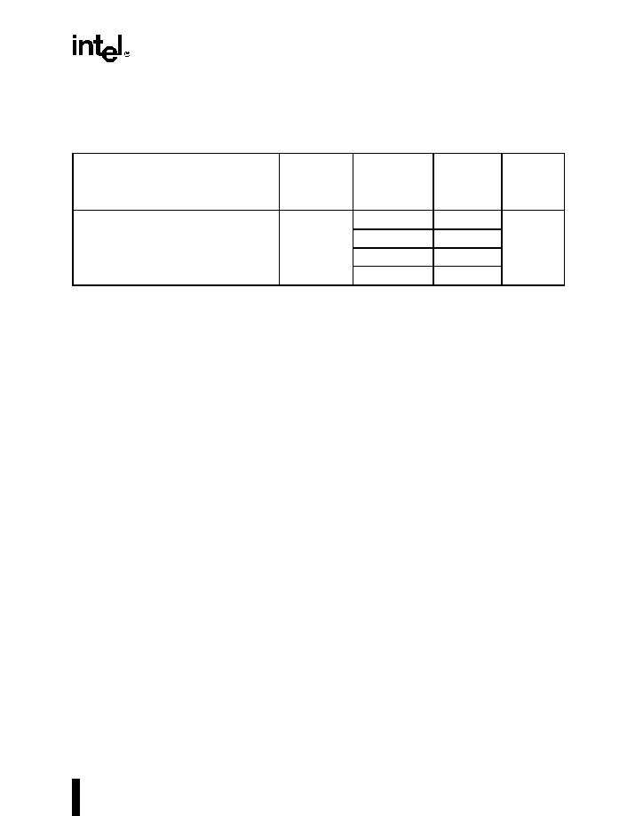
Table 1 shows the embedded ULP Intel486 GX processor and briefly describes its characteristics.
Table 1. The Embedded Ultra-Low Power Intel486
TM
GX Processor
Product
Supply
Voltage
(V
CCP
)
Processor
Core Supply
Voltage
(V
CC
)
Processor
Frequency
(MHz)
Package
FA80486GXSF-33
3.3 V
2.0 V to 3.3 V
16
176-Lead
TQFP
2.2 V to 3.3 V
20
2.4 V to 3.3 V
25
2.7 V to 3.3 V
33
2.0
HOW TO USE THIS DOCUMENT
Even though it has a 16-bit external data bus, the
embedded ULP Intel486 GX processor has charac-
teristics similar to the 32-bit Intel486 SX processor.
This document describes the new features of the
embedded ULP Intel486 GX processor. Some
Intel486 SX processor information is also included to
minimize the dependence on the reference
documents.
For a complete set of documentation related to the
embedded ULP Intel486 GX processor, use this
document in conjunction with the following reference
documents:
∑
Embedded Intel486TM Processor Family
Developer's Manual
-- Order No. 273021
∑
Embedded Intel486TM Processor Hardware
Reference Manual
-- Order No. 273025
∑ Intel Application Note AP-485 --
Intel Processor
Identification with the CPUID Instruction
--
Order No. 241618
3.0
PIN DESCRIPTIONS
3.1
Pin Assignments
The following figures and tables show the pin assign-
ments for the 176-pin Thin Quad Flat Pack (TQFP)
package of the embedded ULP Intel486 GX
processor. Included are:
∑ Figure 2, Package Diagram for 176-Lead TQFP
Package Embedded ULP Intel486TM GX
Processor (pg. 4)
∑ Table 2, Pin Assignment for 176-Lead TQFP
Package Embedded ULP Intel486TM GX
Processor (pg. 5)
∑ Table 3, Pin Cross Reference for 176-Lead TQFP
Package Embedded ULP Intel486TM GX
Processor (pg. 6)
∑ Table 4, Embedded ULP Intel486TM GX Processor
Pin Descriptions (pg. 7)
∑ Table 5, Output Pins (pg. 13)
∑ Table 6, Input/Output Pins (pg. 13)
∑ Table 7, Test Pins (pg. 14)
∑ Table 8, Input Pins (pg. 14)
The tables and figures show "no-connects" as "N/C."
These pins should always remain unconnected.
Connecting N/C pins to V
CC
, V
CCP
, V
SS
, or any other
signal pin can result in component malfunction or
incompatibility with future steppings of the
embedded ULP Intel486 GX processor.
Embedded Ultra-Low Power Intel486TM GX Processor
4
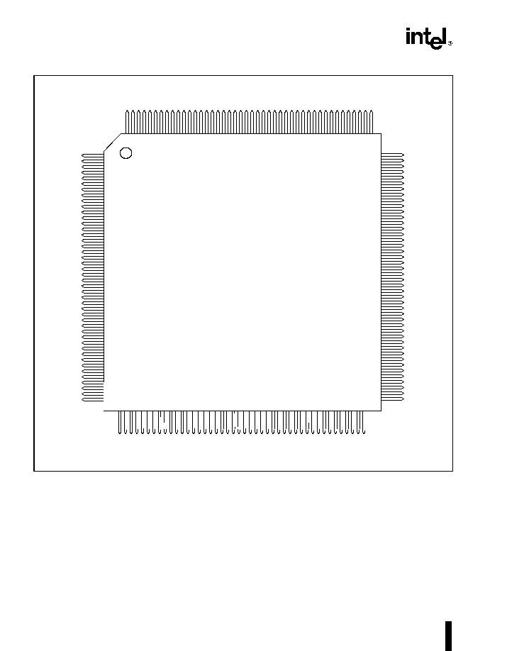
Figure 2. Package Diagram for 176-Lead TQFP Package Embedded ULP Intel486TM GX Processor
1
2
3
4
5
6
7
8
9
10
11
12
13
14
15
16
17
18
19
20
21
22
23
24
25
26
27
28
29
30
31
32
33
34
35
36
37
38
39
40
41
42
43
44
BLAST#
VCC
PLOCK#
LOCK#
VSS
VCCP
N/C
PCHK#
BRDY#
BOFF#
VCC
VSS
N/C
RDY#
KEN#
VCC
VSS
HOLD
AHOLD
TCK
VCC
VCC
VSS
VCC
VCC
CLK
HLDA
W/R#
VSS
VCCP
BREQ
BE0#
BE1#
BE2#
BE3#
VCC
VSS
M/IO#
D/C#
PWT
PCD
VCCP
VSS
VCC
176-Lead TQFP
(top view)
132
131
130
129
128
127
126
125
124
123
122
121
120
119
118
117
116
115
114
113
112
111
110
109
108
107
106
105
104
103
102
101
100
99
98
97
96
95
94
93
92
91
90
89
VSS
VSS
VCCP
A25
A26
A27
A28
VCCP
A29
A30
A31
DP0
D0
D1
D2
D3
D4
VCC
VSS
VCC
VCC
VSS
VCC
VCC
VSS
VCCP
D5
D6
VCCP
N/C
D7
DP1
D8
D9
VSS
VCC
D10
D11
D12
D13
VSS
VCCP
D14
D15
ADS#
A2
VSS
VCCP
VSS
VSS
VCCP
A3
A4
A5
RESERV
E
D#
A6
A7
A8
VSS
VCC
A9
A1
0
VCCP
VSS
VCC
A1
1
A1
2
VCC
A1
3
A1
4
VCCP
VSS
A1
5
A1
6
A1
7
VSS
VCCP
TD
I
TM
S
A1
8
A1
9
A2
0
VCCP
VCCP
A2
1
A2
2
A2
3
A2
4
17
6
17
5
17
4
17
3
17
2
17
1
17
0
16
9
16
8
16
7
16
6
16
5
16
4
16
3
16
2
16
1
16
0
15
9
15
8
15
7
15
6
15
5
15
4
15
3
15
2
15
1
15
0
14
9
14
8
14
7
14
6
14
5
14
4
14
3
14
2
14
1
14
0
13
9
13
8
13
7
13
6
13
5
13
4
13
3
45
46
47
48
54
55
56
57
58
59
60
61
62
63
64
65
66
67
68
69
70
71
72
73
74
75
76
77
78
79
80
81
82
83
84
85
86
87
88
49
50
51
52
53
EADS#
A2
0
M
#
RE
SET
N/
C
N/
C
N/
C
F
L
US
H#
IN
T
R
NM
I
VS
S
VSS
VS
S
VSS
SRES
ET
SM
IA
CT#
VCC
VSS
V
CCP
SM
I#
TD
O
VCC
S
T
PCL
K
#
VS
S
VC
C
VSS
VCC
P
VSS
V
CCP
VSS
VCC
P
N/
C
VSS
VC
C
N/
C
VSS
VSS
V
CCP
VSS
VSS
N/
C
N/
C
N/
C
N/
C
N/
C
Embedded Ultra-Low Power Intel486TM GX Processor
5
Table 2. Pin Assignment for 176-Lead TQFP Package
Embedded ULP Intel486TM GX Processor
Pin #
Description
Pin #
Description
Pin #
Description
Pin #
Description
1
BLAST#
45
EADS#
89
D15
133
A24
2
V
CC
46
A20M#
90
D14
134
A23
3
PLOCK#
47
RESET
91
V
CCP
135
A22
4
LOCK#
48
N/C
92
V
SS
136
A21
5
V
SS
49
N/C
93
D13
137
V
CCP
6
V
CCP
50
N/C
94
D12
138
V
CCP
7
N/C
51
FLUSH#
95
D11
139
A20
8
PCHK#
52
INTR
96
D10
140
A19
9
BRDY#
53
NMI
97
V
CC
141
A18
10
BOFF#
54
V
SS
98
V
SS
142
TMS
11
V
CC
55
V
SS
99
D9
143
TDI
12
V
SS
56
V
SS
100
D8
144
V
CCP
13
N/C
57
V
SS
101
DP1
145
V
SS
14
RDY#
58
SRESET
102
D7
146
A17
15
KEN#
59
SMIACT#
103
N/C
147
A16
16
V
CC
60
V
CC
104
V
CCP
148
A15
17
V
SS
61
V
SS
105
D6
149
V
SS
18
HOLD
62
V
CCP
106
D5
150
V
CCP
19
AHOLD
63
N/C
107
V
CCP
151
A14
20
TCK
64
N/C
108
V
SS
152
A13
21
V
CC
65
SMI#
109
V
CC
153
V
CC
22
V
CC
66
N/C
110
V
CC
154
A12
23
V
SS
67
TDO
111
V
SS
155
A11
24
V
CC
68
V
CC
112
V
CC
156
V
CC
25
V
CC
69
N/C
113
V
CC
157
V
SS
26
CLK
70
N/C
114
V
SS
158
V
CCP
27
HLDA
71
STPCLK#
115
V
CC
159
A10
28
W/R#
72
V
SS
116
D4
160
A9
29
V
SS
73
V
CC
117
D3
161
V
CC
30
V
CCP
74
V
SS
118
D2
162
V
SS
31
BREQ
75
V
CCP
119
D1
163
A8
32
BE0#
76
V
SS
120
D0
164
A7
33
BE1#
77
V
CCP
121
DP0
165
A6
34
BE2#
78
V
SS
122
A31
166
RESERVED#
35
BE3#
79
V
CCP
123
A30
167
A5
36
V
CC
80
N/C
124
A29
168
A4
37
V
SS
81
V
SS
125
V
CCP
169
A3
38
M/IO#
82
V
CC
126
A28
170
V
CCP
39
D/C#
83
N/C
127
A27
171
V
SS
40
PWT
84
V
SS
128
A26
172
V
SS
41
PCD
85
V
SS
129
A25
173
V
CCP
42
V
CCP
86
V
CCP
130
V
CCP
174
V
SS
43
V
SS
87
V
SS
131
V
SS
175
A2
44
V
CC
88
V
SS
132
V
SS
176
ADS#
Embedded Ultra-Low Power Intel486TM GX Processor
6
Table 3. Pin Cross Reference for 176-Lead TQFP Package
Embedded ULP Intel486TM GX Processor
Address
Pin #
Data
Pin #
Control
Pin #
N/C
V
CCP
V
CC
V
SS
A2
175
D0
120
A20M#
46
7
6
2
5
A3
169
D1
119
ADS#
176
13
30
11
12
A4
168
D2
118
AHOLD
19
48
42
16
17
A5
167
D3
117
BE0#
32
49
62
21
23
A6
165
D4
116
BE1#
33
50
75
22
29
A7
164
D5
106
BE2#
34
63
77
24
37
A8
163
D6
105
BE3#
35
64
79
25
43
A9
160
D7
102
BLAST#
1
66
86
36
54
A10
159
D8
100
BOFF#
10
69
91
44
55
A11
155
D9
99
BRDY#
9
70
104
60
56
A12
154
D10
96
BREQ
31
80
107
68
57
A13
152
D11
95
CLK
26
83
125
73
61
A14
151
D12
94
D/C#
39
103
130
82
72
A15
148
D13
93
DP0
121
137
97
74
A16
147
D14
90
DP1
101
138
109
76
A17
146
D15
89
EADS#
45
144
110
78
A18
141
FLUSH#
51
150
112
81
A19
140
HLDA
27
158
113
84
A20
139
HOLD
18
170
115
85
A21
136
INTR
52
173
153
87
A22
135
KEN#
15
156
88
A23
134
LOCK#
4
161
92
A24
133
M/IO#
38
98
A25
129
NMI
53
108
A26
128
PCD
41
111
A27
127
PCHK#
8
114
A28
126
PLOCK#
3
131
A29
124
PWT
40
132
A30
123
RDY#
14
145
A31
122
RESERVED#
166
149
RESET
47
157
SMI#
65
162
SMIACT#
59
171
SRESET
58
172
STPCLK#
71
174
TCK
20
TDI
143
TDO
67
TMS
142
W/R#
28
Embedded Ultra-Low Power Intel486TM GX Processor
7
3.2
Pin Quick Reference
The following is a brief pin description. For detailed signal descriptions refer to Appendix A, "Signal Descrip-
tions," in the
Embedded Intel486TM Processor Family Developer's Manual,
order No. 273021.
Table 4. Embedded ULP Intel486TM GX Processor Pin Descriptions (Sheet 1 of 6)
Symbol
Type
Name and Function
CLK
I
Clock
provides the fundamental timing and internal operating frequency for the
embedded ULP Intel486 GX processor. All external timing parameters are
specified with respect to the rising edge of CLK.
ADDRESS BUS
A31-A4
A3≠A2
I/O
O
Address Lines A31≠A2, together with the byte enable signals, BE3#≠BE0#,
define the physical area of memory or input/output space accessed. Address lines
A31≠A4 are used to drive addresses into the embedded ULP Intel486 GX
processor to perform cache line invalidation. Input signals must meet setup and
hold times t
22
and t
23
. A31≠A2 are not driven during bus or address hold.
BE3#
BE2#
BE1#
BE0#
O
O
O
O
Byte Enable
signals indicate active bytes during read and write cycles. During the
first cycle of a cache fill, the external system should assume that all byte enables
are active. BE3#≠BE0# are active LOW and are not driven during bus hold.
BE3# applies to processor data bits D31≠D24
BE2# applies to processor data bits D23≠D16
BE1# applies to processor data bits D15≠D8
BE0# applies to processor data bits D7≠D0
The byte enables can be used by the external system to generate address bits A1
and A0, as well as byte-high (D15-D8) and byte-low (D7-D0) enables. These are
needed to interpret the 16-bit external data bus.
DATA BUS
D15≠D0
I/O
Data Lines. D7≠D0 define the least significant byte of the data bus; D15-D8 define
the most significant byte of the data bus. These signals must meet setup and hold
times t
22
and t
23
for proper operation on reads. These pins are driven during the
second and subsequent clocks of write cycles.
DP1
DP0
I/O
There is one Data Parity pin for each byte of the data bus. Data parity is generated
on all write data cycles with the same timing as the data driven by the embedded
ULP Intel486 GX processor. Even parity information must be driven back into the
processor on the data parity pins with the same timing as read information to
ensure that the correct parity check status is indicated by the processor. The
signals read on these pins do not affect program execution.
Input signals must meet setup and hold times t
22
and t
23
. DP1 and DP0 must be
connected to V
CCP
through a pull-up resistor in systems that do not use parity. DP1
and DP0 are active HIGH and are driven during the second and subsequent clocks
of write cycles.
Embedded Ultra-Low Power Intel486TM GX Processor
8
PCHK#
O
Parity Status is driven on the PCHK# pin the clock after ready for read operations.
The parity status is for data sampled at the end of the previous clock. A parity error
is indicated by PCHK# being LOW. Parity status is only checked for enabled bytes
as indicated by the byte enable signals. PCHK# is valid only in the clock
immediately after read data is returned to the processor. At all other times PCHK#
is inactive (HIGH). PCHK# is never floated.
BUS CYCLE DEFINITION
M/IO#
D/C#
W/R#
O
O
O
Memory/Input-Output
,
Data/Control
and Write/Read
lines are the primary bus
definition signals. These signals are driven valid as the ADS# signal is asserted.
M/IO#
D/C#
W/R#
Bus Cycle Initiated
0
0
0
Interrupt Acknowledge
0
0
1
HALT/Special Cycle (see details below)
0
1
0
I/O Read
0
1
1
I/O Write
1
0
0
Code Read
1
0
1
Reserved
1
1
0
Memory Read
1
1
1
Memory Write
HALT/Special Cycle
Cycle Name
BE3# - BE0#
A4-A2
Shutdown 1110 000
HALT 1011
000
Stop Grant bus cycle
1011
100
LOCK#
O
Bus Lock
indicates that the current bus cycle is locked. The embedded ULP
Intel486 GX processor does not allow a bus hold when LOCK# is asserted
(address holds are allowed). LOCK# goes active in the first clock of the first locked
bus cycle and goes inactive after the last clock of the last locked bus cycle. The
last locked cycle ends when Ready is returned. LOCK# is active LOW and not
driven during bus hold. Locked read cycles are not transformed into cache fill
cycles when KEN# is returned active.
PLOCK#
O
Pseudo-Lock indicates that the current bus transaction requires more than one
bus cycle to complete. For the embedded ULP Intel486 GX processor, examples of
such operations are segment table descriptor reads (64 bits) and cache line fills
(128 bits).
The embedded ULP Intel486 GX processor drives PLOCK# active until the
addresses for the last bus cycle of the transaction are driven, regardless of
whether RDY# or BRDY# have been returned.
PLOCK# should be sampled only in the clock in which Ready is returned. PLOCK#
is active LOW and is not driven during bus hold.
BUS CONTROL
ADS#
O
Address Status
output indicates that a valid bus cycle definition and address are
available on the cycle definition lines and address bus. ADS# is driven active in the
same clock in which the addresses are driven. ADS# is active LOW and not driven
during bus hold.
Table 4. Embedded ULP Intel486TM GX Processor Pin Descriptions (Sheet 2 of 6)
Symbol
Type
Name and Function
Embedded Ultra-Low Power Intel486TM GX Processor
9
RDY#
I
Non-burst Ready
input indicates that the current bus cycle is complete. RDY#
indicates that the external system has presented valid data on the data pins in
response to a read or that the external system has accepted data from the
embedded ULP Intel486 GX processor in response to a write. RDY# is ignored
when the bus is idle and at the end of the first clock of the bus cycle.
RDY# is active during address hold. Data can be returned to the embedded ULP
Intel486 GX processor while AHOLD is active.
RDY# is active LOW and is not provided with an internal pull-up resistor. RDY#
must satisfy setup and hold times t
16
and t
17
for proper chip operation.
BURST CONTROL
BRDY#
I
Burst Ready
input performs the same function during a burst cycle that RDY#
performs during a non-burst cycle. BRDY# indicates that the external system has
presented valid data in response to a read or that the external system has
accepted data in response to a write. BRDY# is ignored when the bus is idle and at
the end of the first clock in a bus cycle.
BRDY# is sampled in the second and subsequent clocks of a burst cycle. Data
presented on the data bus is strobed into the embedded ULP Intel486 GX
processor when BRDY# is sampled active. If RDY# is returned simultaneously with
BRDY#, BRDY# is ignored and the burst cycle is prematurely aborted.
BRDY# is active LOW and is provided with a small pull-up resistor. BRDY# must
satisfy the setup and hold times t
16
and t
17
.
BLAST#
O
Burst Last
signal indicates that the next time BRDY# is returned, the burst bus
cycle is complete. BLAST# is active for both burst and non-burst bus cycles.
BLAST# is active LOW and is not driven during bus hold.
INTERRUPTS
RESET
I
Reset input forces the embedded ULP Intel486 GX processor to begin execution
at a known state. The processor cannot begin executing instructions until at least
1 ms after V
CC
, V
CCP
, and CLK have reached their proper DC and AC specifica-
tions. The RESET pin must remain active during this time to ensure proper
processor operation. However, for warm resets, RESET should remain active for at
least 15 CLK periods. RESET is active HIGH. RESET is asynchronous but must
meet setup and hold times t
20
and t
21
for recognition in any specific clock.
INTR
I
Maskable Interrupt
indicates that an external interrupt has been generated. When
the internal interrupt flag is set in EFLAGS, active interrupt processing is initiated.
The embedded ULP Intel486 GX processor generates two locked interrupt
acknowledge bus cycles in response to the INTR pin going active. INTR must
remain active until the interrupt acknowledges have been performed to ensure
processor recognition of the interrupt.
INTR is active HIGH and is not provided with an internal pull-down resistor. INTR is
asynchronous, but must meet setup and hold times t
20
and t
21
for recognition in
any specific clock.
Table 4. Embedded ULP Intel486TM GX Processor Pin Descriptions (Sheet 3 of 6)
Symbol
Type
Name and Function
Embedded Ultra-Low Power Intel486TM GX Processor
10
NMI
I
Non-Maskable Interrupt
request signal indicates that an external non-maskable
interrupt has been generated. NMI is rising-edge sensitive and must be held LOW
for at least four CLK periods before this rising edge. NMI is not provided with an
internal pull-down resistor. NMI is asynchronous, but must meet setup and hold
times t
20
and t
21
for recognition in any specific clock.
SRESET
I
Soft Reset pin duplicates all functionality of the RESET pin except that the
SMBASE register retains its previous value. For soft resets, SRESET must remain
active for at least 15 CLK periods. SRESET is active HIGH. SRESET is
asynchronous but must meet setup and hold times t
20
and t
21
for recognition in any
specific clock.
SMI#
I
System Management Interrupt input invokes System Management Mode (SMM).
SMI# is a falling-edge triggered signal which forces the embedded ULP Intel486
GX processor into SMM at the completion of the current instruction. SMI# is
recognized on an instruction boundary and at each iteration for repeat string
instructions. SMI# does not break LOCKed bus cycles and cannot interrupt a
currently executing SMM. The embedded ULP Intel486 GX processor latches the
falling edge of one pending SMI# signal while it is executing an existing SMI#. The
nested SMI# is not recognized until after the execution of a Resume (RSM)
instruction.
SMIACT#
O
System Management Interrupt Active, an active LOW output, indicates that the
embedded ULP Intel486 GX processor is operating in SMM. It is asserted when
the processor begins to execute the SMI# state save sequence and remains active
LOW until the processor executes the last state restore cycle out of SMRAM.
STPCLK#
I
Stop Clock Request input signal indicates a request was made to turn off or
change the CLK input frequency. When the embedded ULP Intel486 GX processor
recognizes a STPCLK#, it stops execution on the next instruction boundary (unless
superseded by a higher priority interrupt), empties all internal pipelines and write
buffers, and generates a Stop Grant bus cycle. STPCLK# is active LOW. Though
STPCLK# has an internal pull-up resistor, an external 10-K
pull-up resistor is
needed if the STPCLK# pin is not used. STPCLK# is an asynchronous signal,
but must remain active until the embedded ULP Intel486 GX processor
issues the Stop Grant bus cycle. STPCLK# may be de-asserted at any time
after the processor has issued the Stop Grant bus cycle.
BUS ARBITRATION
BREQ
O
Bus Request
signal indicates that the embedded ULP Intel486 GX processor has
internally generated a bus request. BREQ is generated whether or not the
processor is driving the bus. BREQ is active HIGH and is never floated.
HOLD
I
Bus Hold Request allows another bus master complete control of the embedded
ULP Intel486 GX processor bus. In response to HOLD going active, the processor
floats most of its output and input/output pins. HLDA is asserted after completing
the current bus cycle, burst cycle or sequence of locked cycles. The embedded
ULP Intel486 GX processor remains in this state until HOLD is de-asserted. HOLD
is active HIGH and is not provided with an internal pull-down resistor. HOLD must
satisfy setup and hold times t
18
and t
19
for proper operation.
Table 4. Embedded ULP Intel486TM GX Processor Pin Descriptions (Sheet 4 of 6)
Symbol
Type
Name and Function
Embedded Ultra-Low Power Intel486TM GX Processor
11
HLDA
O
Hold Acknowledge
goes active in response to a hold request presented on the
HOLD pin. HLDA indicates that the embedded ULP Intel486 GX processor has
given the bus to another local bus master. HLDA is driven active in the same clock
that the processor floats its bus. HLDA is driven inactive when leaving bus hold.
HLDA is active HIGH and remains driven during bus hold.
BOFF#
I
Backoff
input forces the embedded ULP Intel486 GX processor to float its bus in
the next clock. The processor floats all pins normally floated during bus hold but
HLDA is not asserted in response to BOFF#. BOFF# has higher priority than RDY#
or BRDY#; if both are returned in the same clock, BOFF# takes effect. The
embedded ULP Intel486 GX processor remains in bus hold until BOFF# is
negated. If a bus cycle is in progress when BOFF# is asserted the cycle is
restarted. BOFF# is active LOW and must meet setup and hold times t
18
and t
19
for
proper operation.
CACHE INVALIDATION
AHOLD
I
Address Hold
request allows another bus master access to the embedded ULP
Intel486 GX processor's address bus for a cache invalidation cycle. The processor
stops driving its address bus in the clock following AHOLD going active. Only the
address bus is floated during address hold, the remainder of the bus remains
active. AHOLD is active HIGH and is provided with a small internal pull-down
resistor. For proper operation, AHOLD must meet setup and hold times t
18
and t
19
.
EADS#
I
External Address - This signal indicates that a
valid
external address has been
driven onto the embedded ULP Intel486 GX processor address pins. This address
is used to perform an internal cache invalidation cycle. EADS# is active LOW and
is provided with an internal pull-up resistor. EADS# must satisfy setup and hold
times t
12
and t
13
for proper operation.
CACHE CONTROL
KEN#
I
Cache Enable
pin is used to determine whether the current cycle is cacheable.
When the embedded ULP Intel486 GX processor generates a cycle that can be
cached and KEN# is active one clock before RDY# or BRDY# during the first
transfer of the cycle, the cycle becomes a cache line fill cycle. Returning KEN#
active one clock before RDY# during the last read in the cache line fill causes the
line to be placed in the on-chip cache. KEN# is active LOW and is provided with a
small internal pull-up resistor. KEN# must satisfy setup and hold times t
14
and t
15
for proper operation.
FLUSH#
I
Cache Flush
input forces the embedded ULP Intel486 GX processor to flush its
entire internal cache. FLUSH# is active LOW and need only be asserted for one
clock. FLUSH# is asynchronous but setup and hold times t
20
and t
21
must be met
for recognition in any specific clock.
Table 4. Embedded ULP Intel486TM GX Processor Pin Descriptions (Sheet 5 of 6)
Symbol
Type
Name and Function
Embedded Ultra-Low Power Intel486TM GX Processor
12
PAGE CACHEABILITY
PWT
PCD
O
O
Page Write-Through
and Page Cache Disable pins reflect the state of the page
attribute bits, PWT and PCD, in the page table entry, page directory entry or
control register 3 (CR3) when paging is enabled. When paging is disabled, the
embedded ULP Intel486 GX processor ignores the PCD and PWT bits and
assumes they are zero for the purpose of caching and driving PCD and PWT pins.
PWT and PCD have the same timing as the cycle definition pins (M/IO#, D/C#, and
W/R#). PWT and PCD are active HIGH and are not driven during bus hold. PCD is
masked by the cache disable bit (CD) in Control Register 0.
ADDRESS MASK
A20M#
I
Address Bit 20 Mask pin, when asserted, causes the embedded ULP Intel486 GX
processor to mask physical address bit 20 (A20) before performing a lookup to the
internal cache or driving a memory cycle on the bus. A20M# emulates the address
wraparound at 1 Mbyte, which occurs on the 8086 processor. A20M# is active
LOW and should be asserted only when the embedded ULP Intel486 GX
processor is in real mode. This pin is asynchronous but should meet setup and
hold times t
20
and t
21
for recognition in any specific clock. For proper operation,
A20M# should be sampled HIGH at the falling edge of RESET.
TEST ACCESS PORT
TCK
I
Test Clock, an input to the embedded ULP Intel486 GX processor, provides the
clocking function required by the JTAG Boundary scan feature. TCK is used to
clock state information (via TMS) and data (via TDI) into the component on the
rising edge of TCK. Data is clocked out of the component (via TDO) on the falling
edge of TCK. TCK is provided with an internal pull-up resistor.
TDI
I
Test Data Input is the serial input used to shift JTAG instructions and data into the
processor. TDI is sampled on the rising edge of TCK, during the SHIFT-IR and
SHIFT-DR TAP controller states. During all other Test Access Port (TAP) controller
states, TDI is a "don't care." TDI is provided with an internal pull-up resistor.
TDO
O
Test Data Output is the serial output used to shift JTAG instructions and data out
of the component. TDO is driven on the falling edge of TCK during the SHIFT-IR
and SHIFT-DR TAP controller states. At all other times TDO is driven to the high
impedance state.
TMS
I
Test Mode Select is decoded by the JTAG TAP to select test logic operation. TMS
is sampled on the rising edge of TCK. To guarantee deterministic behavior of the
TAP controller, TMS is provided with an internal pull-up resistor.
RESERVED PINS
RESERVED#
I
Reserved is reserved for future use. This pin MUST be connected to an external
pull-up resistor circuit. The recommended resistor value is 10 kOhms.
Table 4. Embedded ULP Intel486TM GX Processor Pin Descriptions (Sheet 6 of 6)
Symbol
Type
Name and Function
Embedded Ultra-Low Power Intel486TM GX Processor
13
Table 5. Output Pins
Name
Active Level
Output Signal
Floated During
Address Hold
Floated During
Bus Hold
During Stop Grant and
Stop Clock States
1
BREQ
HIGH
Previous State
HLDA
HIGH
As per HOLD
BE3#-BE0#
LOW
∑
Previous State
PWT, PCD
HIGH
∑
Previous State
W/R#, M/IO#, D/C#
HIGH/LOW
∑
Previous State
LOCK#
LOW
∑
HIGH (inactive)
PLOCK#
LOW
∑
HIGH (inactive)
ADS#
LOW
∑
HIGH (inactive)
BLAST#
LOW
∑
Previous State
PCHK#
LOW
Previous State
A3-A2
HIGH
∑
∑
Previous State
SMIACT#
LOW
Previous State
NOTES:
1. The term "Previous State" means that the processor maintains the logic level applied to the signal pin just before the pro-
cessor entered the Stop Grant state. This conserves power by preventing the signal pin from floating.
Table 6. Input/Output Pins
Name
Active Level
Output Signal
Floated During
Address Hold
Floated During
Bus Hold
During Stop Grant and
Stop Clock States
1,2
D15-D0
HIGH
∑
Level-Keeper
DP1, DP0
HIGH
∑
Level-Keeper
A31-A4
HIGH
∑
∑
Previous State
NOTES:
1. The term "Level-Keeper" means that the processor maintains the most recent logic level applied to the signal pin. This con-
serves power by preventing the signal pin from floating. If a system component, other than the processor, temporarily drives
these signal pins and then floats them, the processor forces and maintains the most recent logic levels that were applied by
the system component. The level keepers for DP1 and DP0 are always enabled.
2. The term "Previous State" means that the processor maintains the logic level applied to the signal pin just before the pro-
cessor entered the Stop Grant state. This conserves power by preventing the signal pin from floating.
Embedded Ultra-Low Power Intel486TM GX Processor
14
Table 7. Test Pins
Name
Input or Output
Sampled/ Driven On
TCK
Input
N/A
TDI
Input
Rising Edge of TCK
TDO
Output
Failing Edge of TCK
TMS
Input
Rising Edge of TCK
Table 8. Input Pins
Name
Active Level
Synchronous/
Asynchronous
Internal Pull-Up/
Pull-Down
CLK
RESET
HIGH
Asynchronous
SRESET
HIGH
Asynchronous
Pull-Down
HOLD
HIGH
Synchronous
AHOLD
HIGH
Synchronous
Pull-Down
EADS#
LOW
Synchronous
Pull-Up
BOFF#
LOW
Synchronous
Pull-Up
FLUSH#
LOW
Asynchronous
Pull-Up
A20M#
LOW
Asynchronous
Pull-Up
KEN#
LOW
Synchronous
Pull-Up
RDY#
LOW
Synchronous
BRDY#
LOW
Synchronous
Pull-Up
INTR
HIGH
Asynchronous
NMI
HIGH
Asynchronous
RESERVED#
LOW
Asynchronous
Pull-Up
SMI#
LOW
Asynchronous
Pull-Up
STPCLK#
LOW
Asynchronous
Pull-Up
1
TCK
HIGH
Pull-Up
TDI
HIGH
Pull-Up
TMS
HIGH
Pull-Up
1. Though STPCLK# has an internal pull-up resistor, an external 10-K
pull-up resistor is needed if the STPCLK# pin is not
used.

Embedded Ultra-Low Power Intel486TM GX Processor
15
4.0
ARCHITECTURAL AND
FUNCTIONAL OVERVIEW
The embedded ULP Intel486 GX processor archi-
tecture is essentially the same as the 3.3 V Intel486
SX processor with a 1X clock (CLK) input. Refer to
the Embedded Intel486TM Processor Family
Developer's Manual, order number 273021, for a
description of the Intel486 SX processor. The
following notes supplement the information in the
manual.
∑ The embedded ULP Intel486 GX processor has a
16-bit external data bus and two data parity
signals. While it has four byte-enable signals
(BE3#-BE0#), the external system must generate
address bits A1, A0 as well as enables for each
byte of the 16-bit external data bus. More infor-
mation about byte enables is provided in this
datasheet.
∑ The information pertaining to dynamic bus sizing
of the external data bus does not apply. The
embedded ULP Intel486 GX processor does not
have the BS8# signal pin.
∑ The embedded ULP Intel486 GX processor bursts
data cycles similar to an Intel486 SX processor
with bus-sizing BS16# active.
∑ References to "V
CC
" are called "V
CCP
" by the
embedded ULP Intel486 GX processor when the
supply voltage pertains to the processor's external
interface drivers and receivers. The term "V
CC
"
pertains only to the processor core supply voltage
of the embedded ULP Intel486 GX processor.
Information about the split-supply voltage is
provided in this datasheet.
∑ The embedded ULP Intel486 GX processor has
level-keeper circuits for its external 16-bit data bus
(D15-D0) and data parity (DP1, DP0) signals. The
Intel486 SX processor floats these signals instead.
More information about the level-keeper circuitry is
provided in this datasheet.
∑ The manual describes the processor supply-
current consumption for the Auto HALT Power
Down, Stop Grant, and Stop Clock states. This
supply-current consumption for the embedded
ULP Intel486 GX processor is much less than that
of the Intel486 SX processor. Information about
power consumption and these states is provided in
this datasheet.
∑ The CPU ID, Boundary-Scan (JTAG) ID, and
boundary-scan register bits for the embedded ULP
Intel486 GX processor are in this datasheet.
∑ The embedded ULP Intel486 GX processor has
one pin reserved for possible future use. This pin
is an input signal, pin 166. It is called
RESERVED# and must be connected to a 10-K
pull-up resistor.
4.1
Separate Supply Voltages
The embedded ULP Intel486 GX processor has
separate voltage-supply planes for its internal core-
processor circuits and its external driver/receiver
circuits. The supply voltage for the internal core
processor is named V
CC
and the supply voltage for
the external circuits is named V
CCP
.
For a single-supply voltage design, the embedded
ULP Intel486 GX processor is functional at
3.3 V Ī 0.3 V. In this type of system design, the
processor's V
CC
and V
CCP
pins must be tied to the
same power plane.
Even though V
CCP
must be 3.3 V Ī 0.3 V, the
processor's external-output circuits can drive TTL-
compatible components. However, the processor's
external-input circuits do not allow connection to
TTL-compatible components. Section 5.2, DC Speci-
fications (pg. 30) contains the DC specifications for
the processor's input and output signals.
For lower-power operation, a separate, lower voltage
for V
CC
can be chosen, but V
CCP
must be
3.3 V Ī 0.3 V. Any voltage value between 2.0 V and
3.3 V can be chosen for V
CC
for guaranteed
processor operation up to 16 MHz. The embedded
ULP Intel486 GX processor can also operate at
33 MHz, provided the V
CC
value chosen is between
2.7 V and 3.3 V. Section 5.2, DC Specifications (pg.
30) defines supply voltage specifications.
In systems with separate V
CC
and V
CCP
power
planes, the processor-core voltage supply must
always be less than or equal to the processor's
external-interface voltage supply; e.g., the system
design must guarantee:
V
CC
V
CCP
Violating this relationship causes excessive power
consumption. Limited testing has shown no
component damage when this relationship is
violated. However, prolonged violation is not recom-
mended and component integrity is not guaranteed.
The V
CC
V
CCP
relationship must also be
guaranteed by the system design during power-up
and power-down sequences. Refer to Figure 3.
Embedded Ultra-Low Power Intel486TM GX Processor
16
Even though V
CC
must be less than or equal to
V
CCP
, it is recommended that the system's power-on
sequence allows V
CC
to quickly achieve its opera-
tional level once V
CCP
achieves its operational level.
Similarly, the power-down sequence should allow
V
CCP
to power down quickly after V
CC
is below the
operational voltage level.
These recommendations are given to keep power
consumption at a minimum. Deviating from the
recommendations does not create a component
reliability problem, but power consumption of the
processor's external interface circuits increases
beyond normal operating values.
Figure 3. Example of Supply Voltage Power Sequence
4.2
Fast Clock Restart
The embedded ULP Intel486 GX processor has an
integrated proprietary differential delay line (DDL)
circuit for internal clock generation. The DDL is
driven by the CLK input signal provided by the
external system. During normal operation, the
external system must guarantee that the CLK signal
maintains its frequency so that the clock period
deviates no more than 250 ps/CLK. This state,
called the Normal State, is shown in Figure 4.
To increase or decrease the CLK frequency more
quickly than this, the system must interrupt the
processor with the STPCLK# signal. Once the
processor indicates that it is in the Stop Grant State,
the system can adjust the CLK signal to the new
frequency, wait a minimum of eight CLK periods,
then force the processor to return to the normal
operational state by deactivating the STPCLK#
interrupt. This wait of eight CLK periods is much
faster than the 1 ms wait required by earlier Intel486
SX processor products.
While in the Stop Grant State, the external system
may deactivate the CLK signal to the processor. This
forces the processor to the Stop Clock State -- the
state in which the processor consumes the least
power. Once the system reactivates the CLK signal,
the processor transitions to the Stop Grant State
within eight CLK periods.
Normal operation can be resumed by deactivating
the STPCLK# interrupt signal. Here again, the
embedded ULP Intel486 GX processor recovers
from the Stop Clock State much faster than the 1 ms
PLL recovery of earlier Intel486 SX processors.
TIME
V
CCP
V
CC
0 V
V
CC
min
V
CCP
min
V
CC
and V
CCP
(V)
POWER OFF
POWER ON
Embedded Ultra-Low Power Intel486TM GX Processor
17
Figure 4. Stop Clock State Diagram with Typical Power Consumption Values
4 Auto HALT
Power Down State
CLK Running
40 - 85 mWatts
5 Stop Clock Snoop State
1 Normal State
2 Stop Grant State
3 Stop Clock State
EADS#
One Clock PowerUp
Perform Cache Invalidation
Normal Execution
CLK Running
40 - 85 mWatts
Internal Powerdown
CLK Stopped
~ 60 ĶWatts
STPCLK#
deasserted
Stop CLK
Start CLK
plus DDL Startup
Latency
STPCLK# asserted
and Stop Grant bus
cycle generated
STPCLK# asserted and
Stop Grant bus cycle generated
STPCLK# deasserted and
HALT bus cycle generated
HALT asserted and
HALT bus cycle
generated
INTR, NMI, SMI#
RESET, SRESET
EADS#
4.3
Level-Keeper Circuits
To obtain the lowest possible power consumption
during the Stop Grant and Stop Clock states, system
designers must ensure that:
∑ input signals with pull-up resistors are not driven
LOW
∑ input signals with pull-down resistors are not
driven HIGH
See Table 8, Input Pins (pg. 14) for the list of signals
with internal pull-up and pull-down resistors.
All other input pins except A31-A4, D15-D0, DP1,
and DP0 must be driven to the power supply rails to
ensure lowest possible current consumption.
During the Stop Grant and Stop Clock states, most
processor output signals maintain their previous
condition, which is the level they held when entering
the Stop Grant state. In response to HOLD driven
active during the Stop Grant state when the CLK
input is running, the embedded ULP Intel486 GX
processor generates HLDA and floats all output and
input/output signals which are floated during the
HOLD/HLDA state. When HOLD is deasserted,
processor signals which maintain their previous state
return to the state they were in prior to the
HOLD/HLDA sequence.
The data bus (D15-D0) and parity bits also maintain
their previous states during the Stop Grant and Stop
Clock states, but do so differently, as described in
the following paragraphs.

Embedded Ultra-Low Power Intel486TM GX Processor
18
The embedded ULP Intel486 GX processor's data
bus pins (D15-D0) and data parity pins have level
keepers which maintain their previous states while in
the Stop Grant and Stop Clock states. In response to
HOLD driven active during the Stop Grant state
when the CLK input is running, the embedded ULP
Intel486 GX processor generates HLDA and floats
D15-D0, DP1 and DP0 throughout the HOLD/HLDA
cycles. When HOLD is deasserted, the processor's
D15-D0, DP1 and DP0 signals return to the states
they were in prior to the HOLD/HLDA sequence.
At all other times during the Stop Grant and Stop
Clock states, the processor maintains the logic
levels of D15-D0, DP1 and DP0. When the external
system circuitry drives D15-D0, DP1 and DP0 to
different logic levels, the processor flips its D15-D0,
DP1 and DP0 logic levels to match the ones driven
by the external system. The processor maintains
(keeps) these new levels even after the external
circuitry stops driving D15-D0, DP1 and DP0.
For some system designs, external resistors may not
be required on D15-D0, DP1 and DP0 (they are
required on previous Intel486 SX processor
designs). System designs that never request Bus
Hold during the Stop Grant and Stop Clock states
might not require external resistors. If the system
design uses Bus Hold during these states, the
processor disables the level-keepers and floats the
data bus. This type of design would require some
kind of data bus termination to minimize power
consumption. It is strongly recommended that the
D15-D0, DP1 and DP0 pins do not have network
resistors connected. External resistors used in the
system design must be of a sufficient resistance
value to "flip" the level-keeper circuitry and eliminate
potential DC paths.
The level-keeper circuits for DP1 and DP0 are
always enabled, while the level-keeper circuits for
D15-D0 are enabled only during the Stop Grant and
Stop Clock states.
The level-keeper circuit is designed to allow an
external 27-K
pull-up resistor to switch the D15-D0,
DP1 and DP0 circuits to a logic-HIGH level even
though the level-keeper attempts to keep a logic-
LOW level. In general, pull-up resistors smaller than
27 K
can be used as well as those greater than or
equal to 1 M
. Pull-down resistors, when connected
to D15-D0, DP1 and DP0, should be least 800 K
.
4.4
Low-Power Features
As with other Intel486 processors, the embedded
ULP Intel486 GX processor minimizes power
consumption by providing the Auto HALT Power
Down, Stop Grant, and Stop Clock states (see
Figure 4). The embedded ULP Intel486 GX
processor has an Auto Clock Freeze feature that
further conserves power by judiciously deactivating
its internal clocks while in the Normal Execution
Mode. The power-conserving mechanism is
designed such that it does not degrade processor
performance or require changes to AC timing specifi-
cations.
4.4.1
Auto Clock Freeze
To reduce power consumption, during the following
bus cycles -- under certain conditions -- the
processor slows-up or freezes some internal clocks:
∑ Data-Read Wait Cycles (Memory, I/O and Interrupt
Acknowledge)
∑ Data-Write Wait Cycles (Memory, I/O)
∑ HOLD/HLDA Cycles
∑ AHOLD Cycles
∑ BOFF Cycles
Power is conserved during the wait periods in these
cycles until the appropriate external-system signals
are sent to the processor. These signals include:
∑ READY
∑ NMI, SMI#, INTR, and RESET
∑ BOFF#
∑ FLUSH#
∑ EADS#
∑ KEN# transitions
The embedded ULP Intel486 GX processor also
reduces power consumption by temporarily freezing
the clocks of its internal logic blocks. When a logic
block is idle or in a wait state, its clock is frozen.
19
Embedded Ultra-Low Power Intel486TM GX Processor
4.5
Bus Interface and Operation
4.5.1
16-Bit Data Bus
The bi-directional lines, D15-D0, form the data bus
for the embedded ULP Intel486 GX processor. D7-
D0 define the least-significant byte and D15-D8 the
most-significant byte. Data transfers are possible
only to 16-bit devices. Bus-sizing for 8-bit devices
(BS8# signal pin) is not supported by the processor.
In some cases, external circuitry is needed for the
processor to interface with 8-bit devices. An example
of when external circuitry is not needed is an 8-bit
I/O port that is mapped to a byte address. Here only
part of the 16-bit data word is meant for the device
and BS8# is not needed.
D15-D0 are active HIGH. For reads, D15-D0 must
meet the setup and hold times, t
22
and t
23
. D15-D0
are not driven during read cycles and bus hold.
4.5.2
Parity
Parity operation is the same as it is for the rest of the
Intel486 processor family, with these exceptions:
∑ DP0 and DP1 are the data parity pins for the
processor. There is one parity signal for each byte
of the external data bus. Input signals on DP0 and
DP1 must meet the setup and hold times, t
22
and
t
23
. In systems not using parity, DP0 and DP1
must be connected to VCCP through a pull-up
resistor.
∑ The data parity pins have level-keeper circuits
which are described later.
4.5.3
Data Transfer Mechanism
Data transfers operate in a manner similar to data
transfers on the 32-bit data bus members of the
Intel486 processor family with the BS16# pin driven
active. For 32-bit data-bus family members, such 16-
bit data transfers involve all 32 bits of their external
data busses and all four parity bits. Since the
embedded ULP Intel486 GX processor has a 16-bit
external data bus, all data transfers occur on the low
order data bits, D0 through D15. Parity is generated
and checked on DP0 and DP1. Dynamic Data Bus
Sizing (BS16#, and BS8#) is not supported. All
address bits (A31-A2) and byte enables (BE0#,
BE1#, BE2#, and BE3#) are supported. Address bits
A1 and A0 can be generated from the byte-enable
signals in the same manner as the other Intel486
processors. Typically in 16-bit data bus designs, A1,
byte-low enable (BLE), and byte-high enable (BHE)
are needed and can be generated from the four
byte-enable signals. Figure 5 shows the logic that
can be used to generate A1, BHE#, and BLE#.
Figure 5. Logic to Generate A1, BHE# and BLE#
BE0#
BE1#
BE1#
BE3#
BE0#
BE0#
BE1#
BE2#
A1
BHE#
BLE# (or A0)
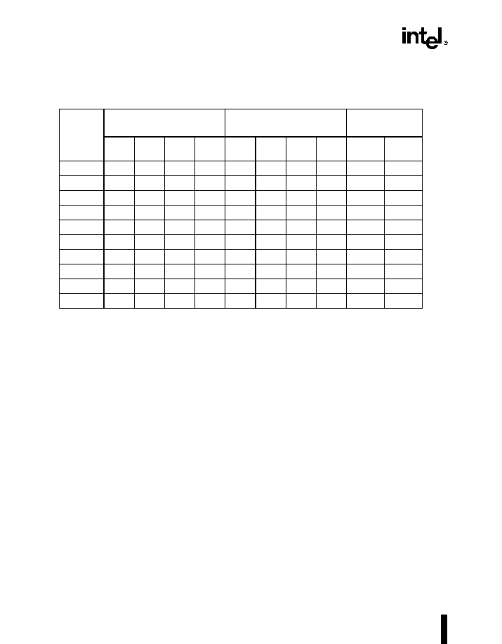
Embedded Ultra-Low Power Intel486TM GX Processor
20
Table 9 contains the list of valid byte-enable combinations and how the 16-bit external data bus is interpreted.
Table 9. Valid Byte-Enable Cycles
Case
Byte Enables
From External Circuitry
(Note 1)
External Data
Bus
BE3#
BE2#
BE1#
BE0#
A1
A0
BHE#
BLE#
(A0)
D15-
D8, DP1
D7-D0,
DP0
1
1
1
1
0
0
0
1
0
-
valid
2
1
1
0
0
0
0
0
0
valid
valid
3
1
0
0
0
0
0
0
0
valid
valid
4
0
0
0
0
0
0
0
0
valid
valid
5
1
1
0
1
0
1
0
1
valid
-
6
1
0
0
1
0
1
0
1
valid
-
7
0
0
0
1
0
1
0
1
valid
-
8
1
0
1
1
1
0
1
0
-
valid
9
0
0
1
1
1
0
0
0
valid
valid
10
0
1
1
1
1
1
0
1
valid
-
NOTES:
1. If the external system indicates to the processor that a read is cacheable, the processor initiates a cache-
line fill. In this case, the external system should ignore BE3#, BE2#, BE1#, and BE0# and force A1, A0, and
BHE# to a low logic level (0) for the first cycle of the transfer. This forces a memory read to start from a data
address having its least significant digit 0, 4, 8, or C (hex). The byte-enable decodes for subsequent cycles
of the line fill follow the table information as listed.
Except for the initial transfer of a cache-line fill, the
Byte Enables BE3#, BE2#, BE1#, and BE0# for
cases 1, 2, 5, 8, 9, and 10 indicate either a one-, or
two-byte data transfer that can be accomplished in
one 16-bit data cycle.
Except for the initial transfer of a cache-line fill, the
Byte Enables BE3#, BE2#, BE1#, and BE0# for
cases 3, 4, 6, and 7 indicate the transfer of two,
three, or four data bytes that cannot be accom-
plished in one 16-bit data cycle. In these cases, the
processor attempts to complete the partial transfer
using an additional data cycle. The additional cycle
could be burst by the processor (processor could
respond with BLAST# unasserted for case 3, 4, 6, or
7). This is true for both memory and I/O reads and
writes. There is more information about bursting in
later sections.
During write cycles, valid data is only driven onto the
external data bus pins corresponding to active byte
enables. Other pins of the data bus are driven but do
not contain valid data.
NOTE:
Unlike the Intel386TM processor, the
embedded ULP Intel486 GX processor
does not duplicate write data onto the parts
of the data bus for which the corre-
sponding byte enable is inactive.

Embedded Ultra-Low Power Intel486TM GX Processor
21
4.5.3.1 Multiple and Burst Cycle Bus Transfers
The embedded ULP Intel486 GX processor, like all
other Intel486 processors, requires more than one
data cycle to read or write data having bit widths
greater than 32. Examples of this data are cache
lines (128 bits) and instruction prefetches (128 bits).
In addition, the embedded ULP Intel486 GX
processor requires multiple data cycles to transfer
data having bit widths greater than 16. An example
is a doubleword operand (32 bits). Transferring mis-
aligned 16-bit words also requires multiple data
cycles.
If a multiple data cycle is a memory-read or I/O-read
data transfer, the processor could use burst cycles to
perform the transfer. The processor could also burst
misaligned 16-bit and 32-bit memory-write or I/O-
write data transfers.
In designing a memory and I/O port controller for the
embedded ULP Intel486 GX processor, knowledge
of the address sequence for burst cycles can be
used to provide high-speed data access (minimal
number of wait states). The following sections
describe this sequence.
4.5.3.2 Cacheable Cycles
The embedded ULP Intel486 GX processor uses
burst cycles to perform a cache line fill. Because of
its 16-bit external data bus, the processor bursts
eight data cycles to read a 128-bit (16-byte) cache
line from system memory. During the first cycle of
the cache line transfer, the external system must
ignore BE3#, BE2#, BE1#, and BE0# presented by
the processor and proceed as if A1, A0, and BHE#
were logic-low levels (0). This forces the memory
read to start from a data address having its least
significant hexadecimal digit 0, 4, 8, or C. The byte
enables presented by the processor for subsequent
cycles are decoded in the usual way by the external
system. The sequences of data addresses are
shown in Table 10. Like the rest of the Intel486
processor family, the initial value of A31-A4, M/IO#,
W/R#, and D/C# are presented by the processor
throughout the cache line fill. Also, the burst
sequence can be terminated by the processor at any
time by with an active BLAST# signal.
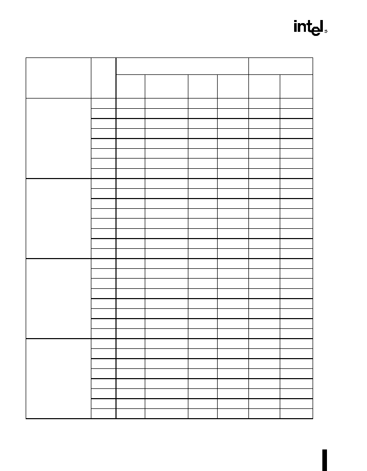
Embedded Ultra-Low Power Intel486TM GX Processor
22
Table 10. Address Sequence for Cache Line Transfers and Instruction Prefetches
Starting Address
(Least significant
hexadecimal digit)
Data
Cycle
Signals from the Processor
Address of
Expected Read Data
A3 A2
Byte
Enables
BE3#-BE0#
A3-A0
(Hex)
BLAST#
D15-D8,
DP1
D7-D-0,
DP0
0, 1, 2, 3
1
0 0
0 0 0 0
0
1
1
0
2
0 0
0 0 1 1
2
1
3
2
3
0 1
0 0 0 0
4
1
5
4
4
0 1
0 0 1 1
6
1
7
6
5
1 0
0 0 0 0
8
1
9
8
6
1 0
0 0 1 1
A
1
B
A
7
1 1
0 0 0 0
C
1
D
C
8
1 1
0 0 1 1
E
0
F
E
4, 5, 6, 7
1
0 1
0 0 0 0
4
1
5
4
2
0 1
0 0 1 1
6
1
7
6
3
0 0
0 0 0 0
0
1
1
0
4
0 0
0 0 1 1
2
1
3
2
5
1 1
0 0 0 0
C
1
D
C
6
1 1
0 0 1 1
E
1
F
E
7
1 0
0 0 0 0
8
1
9
8
8
1 0
0 0 1 1
A
0
B
A
8, 9, A, B
1
1 0
0 0 0 0
8
1
9
8
2
1 0
0 0 1 1
A
1
B
A
3
1 1
0 0 0 0
C
1
D
C
4
1 1
0 0 1 1
E
1
F
E
5
0 0
0 0 0 0
0
1
1
0
6
0 0
0 0 1 1
2
1
3
2
7
0 1
0 0 0 0
4
1
5
4
8
0 1
0 0 1 1
6
0
7
6
C, D, E, F
1
1 1
0 0 0 0
C
1
D
C
2
1 1
0 0 1 1
E
1
F
E
3
1 0
0 0 0 0
8
1
9
8
4
1 0
0 0 1 1
A
1
B
A
5
0 1
0 0 0 0
4
1
5
4
6
0 1
0 0 1 1
6
1
7
6
7
0 0
0 0 0 0
0
1
1
0
8
0 0
0 0 1 1
2
0
3
2
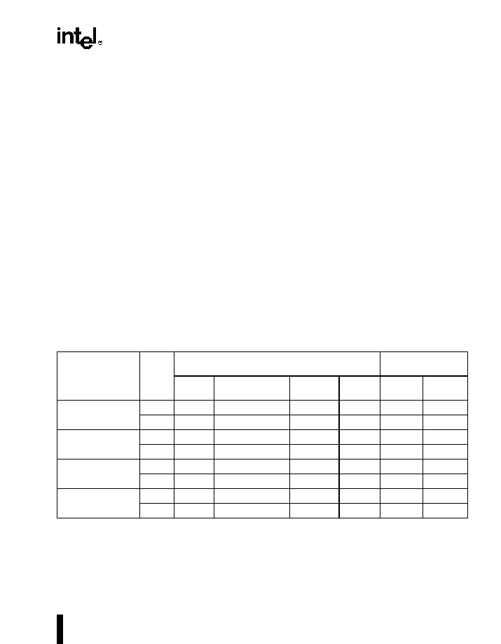
23
Embedded Ultra-Low Power Intel486TM GX Processor
Whenever its cache circuitry is not busy, the
processor uses this same bursting mechanism for
prefetching instructions (128 bits, 16 bytes), even if
the instructions are not indicated as cacheable by
the external system. Instruction prefetches can occur
that use the address sequencing shown in Table 10.
The initial value of A31-A4, M/IO#, W/R#, and D/C#
are presented by the processor throughout the 128-
bit prefetch burst. It is possible for the processor to
prefetch instructions not needed. The burst
sequence can be terminated by the processor at any
time with an active BLAST# signal.
4.5.3.3 Non-Cacheable Cycles
For memory and I/O data transfers, the embedded
ULP Intel486 GX processor determines how many
data cycles are required for the transfer based on its
internal information. This information includes the
byte-length of the data, the transfer's starting data
address, and data alignment. For memory reads, the
processor resorts to the 128-bit cache-line address
sequence described above if the external system
indicates the data is cacheable. Otherwise, the
processor uses its internal information to determine
whether to burst the data cycles of a multiple-cycle
transfer. In some cases, the transfer can be
performed entirely by burst cycles. In other cases, a
combination of burst cycles and single cycles are
required to perform the data transfer. There are also
cases for which burst cycles cannot be used and the
transfer consists of multiple cycles, each beginning
with the ADS# signal.
I/O Writes, I/O Reads, and Memory Writes
If the processor initiates bursting (BLAST# inactive)
during an I/O Write, I/O Read or Memory Write, the
duration of the burst is a maximum of four bytes (32
bits). All of the possible burst situations are listed in
Table 11. In all cases, the burst is two data cycles.
The control signals M/IO#, D/C#, W/R#, address bits
A31-A4 as well as A3 and A2 remain constant
throughout each two-cycle burst.
Table 11. Valid Burst Cycle Sequences - I/O Reads and All Writes
Starting Address
(Least significant
hexadecimal digit)
Data
Cycle
Signals from the Processor
Address of
Expected Read Data
A3 A2
Byte Enables
BE3#-BE0#
A3-A0
(Hex)
BLAST#
D15-D8,
DP1
D7-D-0,
DP0
0, 4, 8, C
1
A3 A2
0 0 0 0
0, 4, 8, C
1
2nd
1st
2
A3 A2
0 0 1 1
2, 6, A, E
0
4th
3rd
1, 5, 9, D
1
A3 A2
0 0 0 1
1, 5, 9, D
1
1st
-
2
A3 A2
0 0 1 1
2, 6, A, E
0
3rd
2nd
1, 5, 9, D
1
A3 A2
1 0 0 1
1, 5, 9, D
1
1st
-
2
A3 A2
1 0 1 1
2, 6, A, E
0
-
2nd
2, 6, A, E
1
A3 A2
1 0 0 0
0, 4, 8, C
1
2nd
1st
2
A3 A2
1 0 1 1
2, 6, A, E
0
-
3rd

Embedded Ultra-Low Power Intel486TM GX Processor
24
Non-Cacheable Memory Reads
When the processor initiates bursting, the duration of
the burst is a maximum of 16 bytes (128 bits).
Non-cacheable instruction prefetches can be 16
bytes in duration. The possible burst sequences are
the same as for cache-line transfers listed in Table
11. The burst sequence can be terminated at any
time with an active BLAST# signal.
The length of a burst transfer can be 16, eight, or
fewer than eight bytes.
For burst lengths of eight or less, the entire burst
transfer is confined to a quad-word (eight-byte) data
boundary of system memory. A31-A3 remain
constant throughout this type of burst transfer.
4.5.3.4 Burst Transfer Address Prediction
The processor provides the data address (A31-A2)
and byte enables (BE3#-BE0#) for the first data
cycle while ADS# is inactive. The initial values for
A1, BHE# and BLE# (A0) can be derived from the
byte enables. If bursting is anticipated, the next data
address can be predicted at this time and can be
used by the memory controller to perform burst data
transfers with minimal wait states. Rather than list all
of the burst mode address combinations, a general
algorithm is provided in Figure 6. This algorithm
holds true for all burst transfers including cache-line
fills, instruction prefetches, I/O and memory-write
data transfers described in earlier sections.
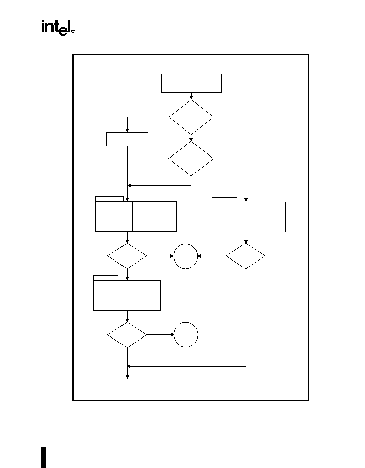
Embedded Ultra-Low Power Intel486TM GX Processor
25
Figure 6. Address Prediction for Burst Transfers (1 of 3)
BLAST# = 1?
BLAST# = 1?
Define LA3 and LA2 as the
initial A3 and A2 values
Begin when ADS# is active
Cacheable?
Indicate "cacheable
data" to processor
BE3# - BE0# =
xx11?
First Transfer
MA3=LA3
MA2=LA2
MA1=0
Next Transfer
(After processor
returns BLAST#=1)
MA3=LA3
MA2=LA2
MA1=1
Data Cycle
First Transfer
MA3=LA3
MA2=LA2
MA1=1
Next Transfer
(After processor
returns BLAST#=1)
MA3=LA3
MA2=Not [LA2]
MA1=0
Data Cycle
No
Yes
No
Yes
END
No
No
Yes
Yes
Next Transfer
MA3=LA3
MA2=Not [LA2]
MA1=0
Data Cycle
BLAST# = 1?
No
END
Yes
Continued
Embedded Ultra-Low Power Intel486TM GX Processor
26
Figure 7. Address Prediction for Burst Transfers (2 of 3)
Continued from previous figure
Next Transfer
MA3=LA3
MA2=Not [LA2]
MA1=1
Data Cycle
BLAST# = 1?
No
END
Yes
Next Transfer
MA3=Not [LA3]
MA2=LA2
MA1=0
Data Cycle
BLAST# = 1?
No
END
Next Transfer
MA3=Not [LA3]
MA2=LA2
MA1=1
Data Cycle
BLAST# = 1?
No
END
Yes
Next Transfer
MA3=Not [LA3]
MA2=Not [LA2]
MA1=0
Data Cycle
BLAST# = 1?
No
END
Continued
Yes
Yes
Embedded Ultra-Low Power Intel486TM GX Processor
27
Figure 8. Address Prediction for Burst Transfers (3 of 3)
Next Transfer
MA3=Not [LA3]
MA2=Not [LA2]
MA1=1
Data Cycle
BLAST# = 1?
No
END
Yes
This is the last transfer. There is
no need to predict the next
address
Data Cycle
Continued from previous figure
In the figure, MA3, MA2, and MA1 are memory
address bits. LA3 and LA2 are the saved, initial
values of A3 and A2 respectively. The term "MA2 =
NOT [LA2]" means that MA2 is the opposite logic
state as the saved initial A2 value. MA31-MA4 are
derived directly from A31-A4, which remain constant
throughout the burst transfer. M/IO#, W/R#, and
D/C# also remain constant. BLE# (A0) is not shown,
but is always active (LOW) throughout the transfer.
BHE#, also not shown, cannot be predicted for the
last data cycle of a burst transfer and must be
decoded from the byte enable bits for the last burst
cycle (follows BLAST# = 0). Otherwise BHE# is
always active (LOW) throughout the burst. The
processor defines "cacheable data" as the case
where PCD is inactive (LOW) and LOCK# is inactive
(HIGH) and KEN# is active (LOW).
4.6
CPUID Instruction
The embedded ULP Intel486 GX processor supports
the CPUID instruction (see Table 12). Because not
all Intel processors support the CPUID instruction, a
simple test can determine if the instruction is
supported. The test involves the processor's ID Flag,
which is bit 21 of the EFLAGS register. If software
can change the value of this flag, the CPUID
instruction is available. The actual state of the ID
Flag bit is irrelevant and provides no significance to
the hardware. This bit is cleared (reset to zero) upon
device reset (RESET or SRESET) for compatibility
with Intel486 processor designs that do not support
the CPUID instruction.
CPUID-instruction details are provided here for the
embedded ULP Intel486 GX processor. Refer to
Intel Application Note AP-485
Intel Processor Identi-
fication with the CPUID Instruction
(Order No.
241618) for a description that covers all aspects of
the CPUID instruction and how it pertains to other
Intel processors.
4.6.1
Operation of the CPUID Instruction
The CPUID instruction requires the software
developer to pass an input parameter to the
processor in the EAX register. The processor
response is returned in registers EAX, EBX, EDX,
and ECX.
Embedded Ultra-Low Power Intel486TM GX Processor
28
Vendor ID String - When the parameter passed in EAX is 0 (zero), the register values returned upon
instruction execution are shown in the following table.
The values in EBX, EDX and ECX indicate an Intel processor. When taken in the proper order, they decode to
the string "
GenuineIntel
."
Table 12. CPUID Instruction Description
OP CODE
Instruction
Processor
Core Clocks
Parameter passed in
EAX
(Input Value)
Description
0F A2
CPUID
9
0
Vendor (Intel) ID String
14
1
Processor Identification
9
> 1
Undefined (Do Not Use)
31-------------24
23-----------16
15--------------8
7--------------0
High Value (= 1)
EAX
0 0 0 0
0 0 0 0
0 0 0 0
0 0 0 1
Vendor ID String
EBX
u
(75)
n
(6E)
e
(65)
G
(47)
(ASCII
EDX
I
(49)
e
(65)
n
(6E)
i
(69)
Characters)
ECX
l
(6C)
e
(65)
t
(74)
n
(6E)
Processor Identification - When the parameter
passed to EAX is 1 (one), the register values
returned upon instruction execution are:
31---------------------------14
13,12
11----8
7----4
3----0
Processor
Signature
EAX
(Do Not Use)
Intel Reserved
0 0
Processor
Type
0 1 0 0
Family
0 0 1 0
Model
XXXX
Stepping
(Intel releases information about stepping numbers as needed)
31--------------------------------------------------------------------------------------------------0
Intel Reserved
EBX
Intel Reserved
(Do Not Use)
ECX
Intel Reserved
31----------------------------------------------------------------------------2
1
0
Feature Flags
EDX
0------------------------------------------------------------------------------0
1
VME
0
FPU
Embedded Ultra-Low Power Intel486TM GX Processor
29
4.7
Identification After Reset
Processor Identification - Upon reset, the EDX register contains the processor signature:
4.8
Boundary Scan (JTAG)
4.8.1
Device Identification
Table 13 shows the 32-bit code for the embedded ULP Intel486 GX processor which is loaded into the Device
Identification Register.
31---------------------------14
13,12
11----8
7----4
3----0
Processor
Signature
EDX
(Do Not Use)
Intel Reserved
0 0
Processor
Type
0 1 0 0
Family
0 0 1 0
Model
XXXX
Stepping
(Intel releases information about stepping numbers as needed)
Table 13. Boundary Scan Component Identification Code
Version
Part Number
Mfg ID
009H = Intel
1
V
CC
0=5V
1=3.3 V
Intel
Architecture
Type
Family
0100 = Intel486
CPU Family
Model
=
embedded ULP
Intel486 GX
processor
31----28
27
26-----------21
20----17
16--------12
11------------1
0
XXXX
1
000001
0100
00000001001
1
(Intel releases information about version numbers as needed)
Boundary Scan Component Identification Code = x828 4013 (Hex)
4.8.2
Boundary Scan Register Bits and Bit
Order
The boundary scan register contains a cell for each
pin as well as cells for control of bidirectional and
three-state pins. There are "Reserved" bits which
correspond to no-connect (N/C) signals of the
embedded ULP Intel486 GX processor. Control
registers WRCTL, ABUSCTL, BUSCTL, and
MISCCTL are used to select the direction of bidirec-
tional or three-state output signal pins. A "1" in these
cells designates that the associated bus or bits are
floated if the pins are three-state, or selected as
input if they are bidirectional.
∑ WRCTL controls D15-D0, DP1 and DP0
∑ ABUSCTL controls A31-A2
∑ BUSCTL controls ADS#, BLAST#, PLOCK#,
LOCK#, W/R#, BE0#, BE1#, BE2#, BE3#, M/IO#,
D/C#, PWT, and PCD
∑ MISCCTL controls PCHK#, HLDA, and BREQ
Embedded Ultra-Low Power Intel486TM GX Processor
30
The following is the bit order of the embedded ULP Intel486 GX processor boundary scan register:
TDO
A2, A3, A4, A5, RESERVED, A6, A7, A8, A9, A10, A11, A12, A13, A14, A15, A16, A17,
A18, A19, A20, A21, A22, A23, A24, A25, A26, A27, A28, A29, A30, A31, DP0, D0, D1,
D2, D3, D4, D5, D6, D7, DP1, D8, D9, D10, D11, D12, D13, D14, D15, Reserved,
Reserved, Reserved, Reserved, Reserved, Reserved, Reserved, Reserved, Reserved,
Reserved, Reserved, Reserved, Reserved, Reserved, Reserved, Reserved, Reserved,
Reserved, STPCLK#, Reserved, Reserved, SMI#, SMIACT#, SRESET, NMI, INTR,
FLUSH#, RESET, A20M#, EADS#, PCD, PWT, D/C#, M/IO#, BE3#, BE2#, BE1#, BE0#,
BREQ, W/R#, HLDA, CLK, Reserved, AHOLD, HOLD, KEN#, RDY#, Reserved,
Reserved, BOFF#, BRDY#, PCHK#, LOCK#, PLOCK#, BLAST#, ADS#, MISCCTL,
BUSCTL, ABUSCTL, WRCTL
TDI
5.0
ELECTRICAL SPECIFICATIONS
5.1
Maximum Ratings
Table 14 is a stress rating only. Extended exposure
to the Maximum Ratings may affect device reliability.
Furthermore, although the embedded ULP Intel486
GX processor contains protective circuitry to resist
damage from electrostatic discharge, always take
precautions to avoid high static voltages or electric
fields.
Functional operating conditions are given in Section
5.2, DC Specifications and Section 5.3, AC Speci-
fications.
5.2
DC Specifications
The following tables show the operating supply
voltages, DC I/O specifications, and component
power consumption for the embedded ULP Intel486
GX processor.
Table 14. Absolute Maximum Ratings
Case Temperature under
Bias
-65 įC to +110 įC
Storage Temperature
-65 įC to +150 įC
DC Voltage on Any Pin
with Respect to Ground
-0.5 V to V
CCP
+ 0.5 V
Supply Voltage V
CC
with
Respect to V
SS
-0.5 V to +4.6 V
Supply Voltage V
CCP
with Respect to V
SS
-0.5 V to +4.6 V
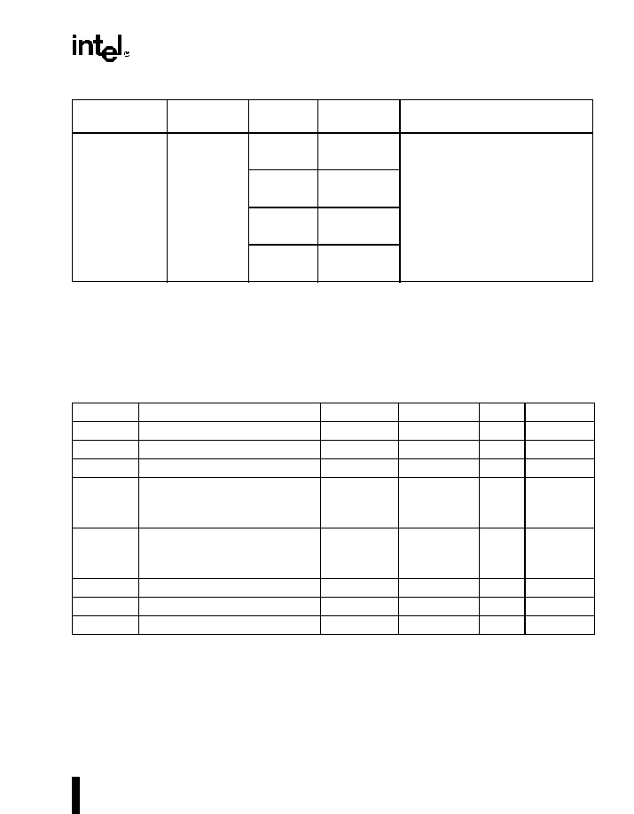
Embedded Ultra-Low Power Intel486TM GX Processor
31
Table 15. Operating Supply Voltages
Product
V
CCP
Range
1
Max. CLK
Frequency
V
CC
Range
2
V
CC
Fluctuation
FA80486GXSF-33
3.3 V
Ī
0
.
3 V
16
2.0 V min
3.3 V max
Ī
0.2 V
+0.3 V/-0.2 V
Ī
0.3 V
at 2.0 V
V
CC
2.7 V
at 2.7 V
<
V
CC
< 3.0 V
at 3.0 V
V
CC
3.3 V
20
2.2 V min
3.3 V max
25
2.4 V min
3.3 V max
33
2.7 V min
3.3 V max
NOTES:
1. In all cases, V
CCP
must be
V
CC
.
2. V
CC
may be set to any voltage within the V
CC
Range. The setting determines the allowed V
CC
Fluctuation.
Table 16. DC Specifications (Sheet 1 of 2)
T
CASE
=0 įC to +85 įC
Symbol
Parameter
Min.
Max.
Unit
Notes
V
IL
Input LOW Voltage
-0.3
+0.8
V
V
IH
Input HIGH Voltage
2.0
V
CCP
+0.3
V
Note 1
V
IHC
Input HIGH Voltage of CLK
V
CCP
-0.6
V
CCP
+0.3
V
V
OL
Output LOW Voltage
I
OL
= 2.0 mA
I
OL
= 100 ĶA
0.4
0.2
V
V
V
OH
Output HIGH Voltage
I
OH
= -2.0 mA
I
OH
= -100 ĶA
2.4
V
CCP
-0.2
V
V
I
LI
Input Leakage Current
15
Ķ
A
Note 2
I
IH
Input Leakage Current
200
Ķ
A
Note 3
I
IL
Input Leakage Current
400
Ķ
A
Note 4
NOTES:
1. All inputs except CLK.
2. This parameter is for inputs without pull-up or pull-down resistors and 0V
V
IN
V
CCP
.
3. This parameter is for inputs with pull-down resistors and V
IH
= 2.4V, and for level-keeper pins at V=0.4V.
4. This parameter is for inputs with pull-up resistors and V
IL
= 0.4V, and for level-keeper pins at V=2.4V.
5. F
C
=1 MHz. Not 100% tested.
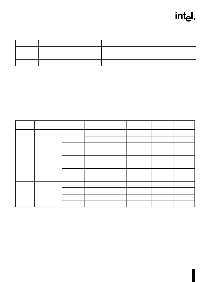
Embedded Ultra-Low Power Intel486TM GX Processor
32
I
LO
Output Leakage Current
15
Ķ
A
C
IN
Input Capacitance
10
pF
Note 5
C
OUT
I/O or Output Capacitance
10
pF
Note 5
C
CLK
CLK Capacitance
6
pF
Note 5
Table 17. Active I
CC
Values
T
CASE
=0 įC to +85 įC
Symbol
Parameter
Frequency
Supply Voltage
Typical I
CC
Max. I
CC
Notes
I
CC1
I
CC
Active
(V
CC
pins)
16 MHz
V
CC
= 2.0
Ī
0.2 V
65 mA
105 mA
V
CC
= 3.3
Ī
0.3 V
105 mA
170 mA
20 MHz
V
CC
= 2.2
Ī
0.2 V
85 mA
140 mA
V
CC
= 3.3
Ī
0.3 V
130 mA
210 mA
25 MHz
V
CC
= 2.4
Ī
0.2 V
120 mA
195 mA
V
CC
= 3.3
Ī
0.3 V
165 mA
260 mA
33 MHz
V
CC
= 2.7
Ī
0.2 V
180 mA
280 mA
V
CC
= 3.3
Ī
0.3 V
220 mA
345 mA
I
CC2
I
CC
Active
(V
CCP
pins)
16 MHz
V
CCP
= 3.3
Ī
0.3 V
5 mA
16 mA
1
20 MHz
V
CCP
= 3.3
Ī
0.3 V
6 mA
20 mA
1
25 MHz
V
CCP
= 3.3
Ī
0.3 V
9 mA
30 mA
1
33 MHz
V
CCP
= 3.3
Ī
0.3 V
12 mA
40 mA
1
NOTES:
1. These parameters are for C
L
= 50 pF
Table 16. DC Specifications (Sheet 2 of 2)
T
CASE
=0 įC to +85 įC
NOTES:
1. All inputs except CLK.
2. This parameter is for inputs without pull-up or pull-down resistors and 0V
V
IN
V
CCP
.
3. This parameter is for inputs with pull-down resistors and V
IH
= 2.4V, and for level-keeper pins at V=0.4V.
4. This parameter is for inputs with pull-up resistors and V
IL
= 0.4V, and for level-keeper pins at V=2.4V.
5. F
C
=1 MHz. Not 100% tested.
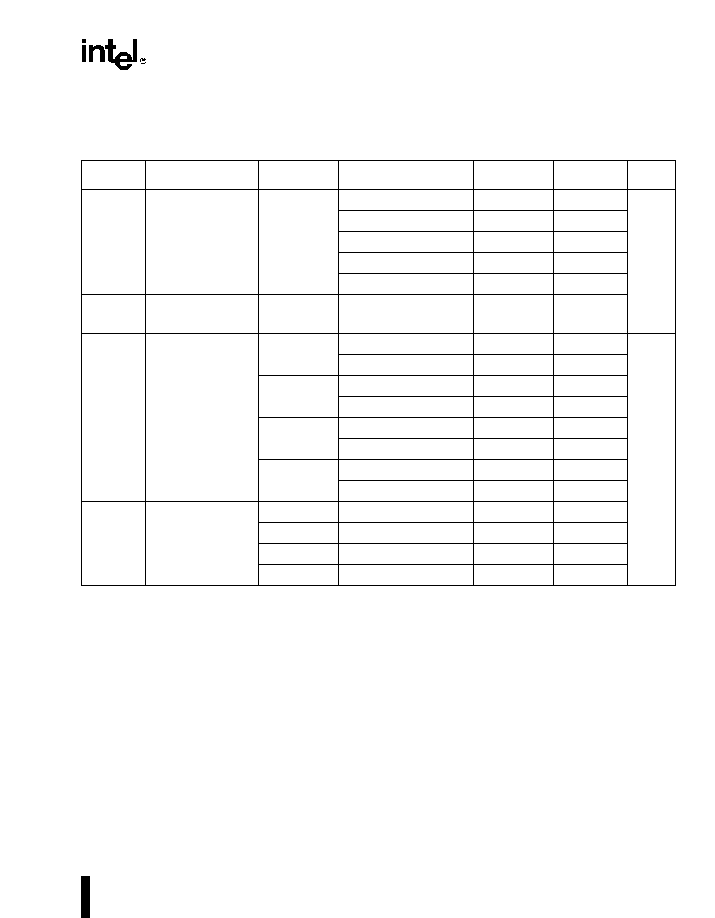
Embedded Ultra-Low Power Intel486TM GX Processor
33
Table 18. Clock Stop, Stop Grant, and Auto HALT Power Down I
CC
Values
T
CASE
= 0 įC to +85 įC
Symbol
Parameter
Frequency
Supply Voltage
Typical I
CC
Max. I
CC
Notes
I
CCS0
I
CC
Stop Clock
(V
CC
pins)
0 MHz
V
CC
= 2.0
Ī
0.2 V
3
Ķ
A
105
Ķ
A
Note 1
V
CC
= 2.2
Ī
0.2 V
3
Ķ
A
110
Ķ
A
V
CC
= 2.4
Ī
0.2 V
4
Ķ
A
120
Ķ
A
V
CC
= 2.7
Ī
0.2 V
4
Ķ
A
130
Ķ
A
V
CC
= 3.3
Ī
0.3 V
5
Ķ
A
150
Ķ
A
I
CCS2
I
CC
Stop Clock
(V
CCP
pins)
0 MHz
V
CCP
= 3.3
Ī
0.3 V
3
Ķ
A
80
Ķ
A
I
CCS1
I
CC
Stop Grant,
Auto HALT
Power Down
(V
CC
pins)
16 MHz
V
CC
= 2.0
Ī
0.2 V
8 mA
15 mA
V
CC
= 3.3
Ī
0.3 V
12 mA
20 mA
20 MHz
V
CC
= 2.2
Ī
0.2 V
10 mA
20 mA
V
CC
= 3.3
Ī
0.3 V
15 mA
25 mA
25 MHz
V
CC
= 2.4
Ī
0.2 V
14 mA
25 mA
V
CC
= 3.3
Ī
0.3 V
20 mA
30 mA
33 MHz
V
CC
= 2.7
Ī
0.2 V
20 mA
30 mA
V
CC
= 3.3
Ī
0.3 V
25 mA
35 mA
I
CCS3
I
CC
Stop Grant,
Auto HALT
Power Down
(V
CCP
pins)
16 MHz
V
CCP
= 3.3
Ī
0.3 V
270
Ķ
A
1.0 mA
20 MHz
V
CCP
= 3.3
Ī
0.3 V
340
Ķ
A
1.2 mA
25 MHz
V
CCP
= 3.3
Ī
0.3 V
425
Ķ
A
1.5 mA
33 MHz
V
CCP
= 3.3
Ī
0.3 V
610
Ķ
A
2.0 mA
NOTES:
1. The I
CC
Stop Clock specification refers to the I
CC
value once the processor enters the Stop Clock state. For all input signals,
the V
IH
and V
IL
levels must be equal to V
CCP
and 0V, respectively, to meet the I
CC
Stop Clock specifications.
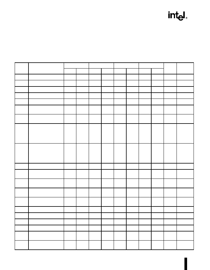
Embedded Ultra-Low Power Intel486TM GX Processor
34
5.3
AC Specifications
The AC specifications for the embedded ULP Intel486 GX processor are given in this section.
Table 19. AC Characteristics (Sheet 1 of 2)
valid over the operating supply voltages listed in Table 15, Operating Supply Voltages (pg. 31).
T
CASE
= 0 įC to +85 įC; C
L
= 50 pF
Symbol
Parameter
2.0V
V
CC
<
2.2V
2.2V
V
CC
<
2.4V
2.4V
V
CC
<
2.7V
2.7V
V
CC
3.3V
Min
Max
Min
Max
Min
Max
Min
Max
Unit
Notes
Frequency
0
16
0
20
0
25
0
33
MHz
Note 1
t
1
CLK Period
62.5
50
40
30
ns
Note 1
t
1a
CLK Period Stability
250
250
250
250
ps/CLK
Note 2
t
2
CLK High Time
23
18
14
11
ns
at 2V
t
3
CLK Low Time
23
18
14
11
ns
at 0.8V
t
4
CLK Fall Time
4
4
4
3
ns
2V to 0.8V
Note 3
t
5
CLK Rise Time
4
4
4
3
ns
0.8V to 2V
Note 3
t
6
A2-A31, PWT, PCD,
BE0#-BE3#, M/IO#,
D/C#, W/R#, ADS#,
LOCK#, BREQ, HLDA,
SMIACT# Valid Delay
3
30
3
24
3
19
3
16
ns
t
7
A2-A31, PWT, PCD,
BE0#-BE3#, M/IO#,
D/C#, W/R#, ADS#,
LOCK#, BREQ, Float
Delay
36
30
28
20
ns
Note 3
t
8
PCHK# Valid Delay
3
34
3
29
3
24
3
22
ns
t
8a
BLAST#, PLOCK# Valid
Delay
3
34
3
29
3
24
3
20
ns
t
9
BLAST#, PLOCK# Float
Delay
36
30
28
20
ns
Note 3
t
10
D0-D15, DP0, DP1
Write Delay
3
31
3
26
3
20
3
19
ns
t
11
D0-D15, DP0, DP1
Float Delay
36
30
28
20
ns
Note 3
t
12
EADS# Setup Time
13
11
8
6
ns
t
13
EADS# Hold Time
4
4
3
3
ns
t
14
KEN# Setup Time
13
11
8
6
ns
t
15
KEN# Hold Time
4
4
3
3
ns
t
16
RDY#, BRDY# Setup
Time
13
11
8
6
ns
t
17
RDY#, BRDY# Hold
Time
4
4
3
3
ns
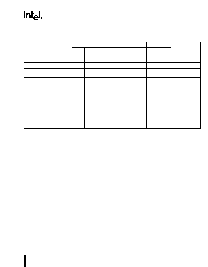
Embedded Ultra-Low Power Intel486TM GX Processor
35
.
t
18
HOLD, AHOLD Setup
Time
15
13
10
6
ns
t
18a
BOFF# Setup Time
15
13
10
9
ns
t
19
HOLD, AHOLD, BOFF#
Hold Time
4
4
3
3
ns
t
20
FLUSH#, A20M#, NMI,
INTR, SMI#, STPCLK#,
SRESET, RESET Setup
Time
15
13
10
6
ns
t
21
FLUSH#, A20M#, NMI,
INTR, SMI#, STPCLK#,
SRESET, RESET Hold
Time
4
4
3
3
ns
t
22
D0-D15, DP0, DP1, A4-
A31 Read Setup Time
11
8
6
6
ns
t
23
D0-D15, DP0, DP1, A4-
A31 Read Hold Time
4
4
3
3
ns
NOTE:
1. 0 Hz operation is tested and guaranteed by the STPCLK# and Stop Grant bus cycle protocol. 0 Hz < CLK < 8 MHz operation is
confirmed by design characterization, but not 100% tested in production.
2. Specification t1a is applicable only when
STPCLK# / STOP GRANT bus cycle protocol.
3. Not 100% tested, guaranteed by design characterization.
4. CLK reference voltage for timing measurement is 1.5 V except t2 through t5. Other signals are measured at 1.5 V.
Table 19. AC Characteristics (Sheet 2 of 2)
valid over the operating supply voltages listed in Table 15, Operating Supply Voltages (pg. 31).
T
CASE
= 0 įC to +85 įC; C
L
= 50 pF
Symbol
Parameter
2.0V
V
CC
<
2.2V
2.2V
V
CC
<
2.4V
2.4V
V
CC
<
2.7V
2.7V
V
CC
3.3V
Min
Max
Min
Max
Min
Max
Min
Max
Unit
Notes
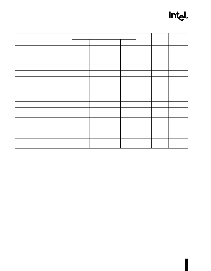
Embedded Ultra-Low Power Intel486TM GX Processor
36
Table 20. AC Specifications for the Test Access Port
Symbol
Parameter
1.8 V
Vcc
<
3.0 V Vcc = 3.3 Ī 0.3 V
Unit
Figure
Notes
Min
Max
Min
Max
t
24
TCK Frequency
5
8
MHz
15
t
25
TCK Period
200
125
ns
15
Note 1
t
26
TCK High Time
65
40
ns
15
@ 2.0V
t
27
TCK Low Time
65
40
ns
15
@0.8V
t
28
TCK Rise Time
15
8
ns
15
Note 2
t
29
TCK Fall Time
15
8
ns
15
Note 2
t
30
TDI, TMS Setup Time
16
8
ns
16
Note 3
t
31
TDI, TMS Hold Time
20
10
ns
16
Note 3
t
32
TDO Valid Delay
3
46
3
30
ns
16
Note 3
t
33
TDO Float Delay
52
36
ns
16
Notes 3, 4
t
34
All Outputs (except
TDO) Valid Delay
3
80
3
30
ns
16
Note 3
t
35
All Outputs (except
TDO) Float Delay
88
36
ns
16
Notes 3, 4
t
36
All Inputs (except TDI,
TMS, TCK) Setup Time
16
8
ns
16
Note 3
t
37
All Inputs (except TDI,
TMS, TCK) Hold Time
35
15
ns
16
Note 3
NOTES:
1. TCK period
CLK period.
2. Rise/Fall Times are measured between 0.8 V and 2.0 V. Rise/Fall times can be relaxed by 1 ns per 10 ns increase in TCK
period.
3. Parameter measured from TCK.
4. Not 100% tested, guaranteed by design characterization.
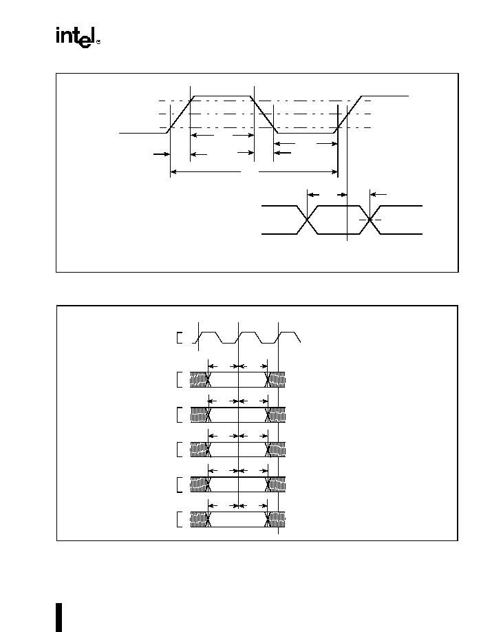
Embedded Ultra-Low Power Intel486TM GX Processor
37
Figure 9. CLK Waveform
Figure 10. Input Setup and Hold Timing
1.5 V
t
1
t
5
t
2
t
4
t
3
0.8 V
CLK
2.0 V
t
x
t
y
1.5 V
t
x
= input setup times
t
y
= input hold times, output float, valid and hold times
1.5 V
0.8 V
2.0 V
t
12
T
x
T
x
T
x
T
x
CLK
EADS#
KEN#
BOFF#, AHOLD, HOLD
RESET, FLUSH#,
A4-A31
(READ)
A20M#, INTR, NMI,
SMI#, STPCLK#, SRESET
t
13
t
15
t
14
t
19
t
18
t
21
t
20
t
23
t
22
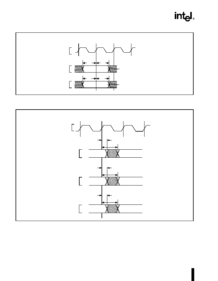
Embedded Ultra-Low Power Intel486TM GX Processor
38
Figure 11. Input Setup and Hold Timing
Figure 12. Output Valid Delay Timing
T
2
T
x
CLK
RDY#, BRDY#
D15-D0, DP0, DP1
T
x
1.5 V
1.5 V
t
17
t
16
t
22
t
23
BLAST#,
PLOCK#
T
x
T
x
T
x
T
x
CLK
A2-A31, PWT, PCD,
D15-D0, DP0, DP1
VALID n+1
MAX
t
6
VALID n
t
10
t
8a
BE0-3#, M/IO#,
D/C#, W/R#, ADS#,
LOCK#, BREQ, HLDA,
VALID n+1
MIN
MAX
VALID n
VALID n+1
MIN
MAX
VALID n
MIN
SMIACT#
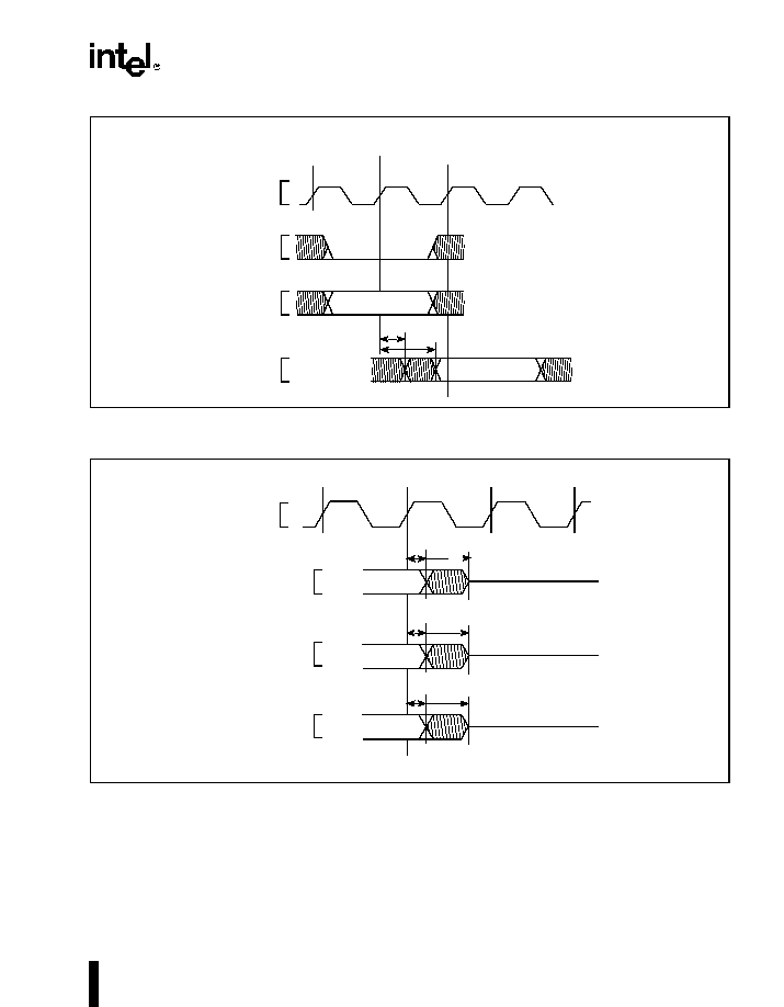
Embedded Ultra-Low Power Intel486TM GX Processor
39
Figure 13. PCHK# Valid Delay Timing
Figure 14. Maximum Float Delay Timing
RDY#, BRDY#
D0-D15
DP0, DP1
VALID
MIN
MAX
t
8
PCHK#
T
x
T
x
T
x
T
x
CLK
VALID
T
x
T
x
T
x
CLK
A2-A31, PWT, PCD,
D15-D0, DP0, DP1
BLAST#,
MIN
t
6
VALID
BE0-3#, M/IO#,
D/C#, W/R#, ADS#,
LOCK#, BREQ
PLOCK#
t
7
t
10
t
11
t
8a
t
9
MIN
VALID
MIN
VALID
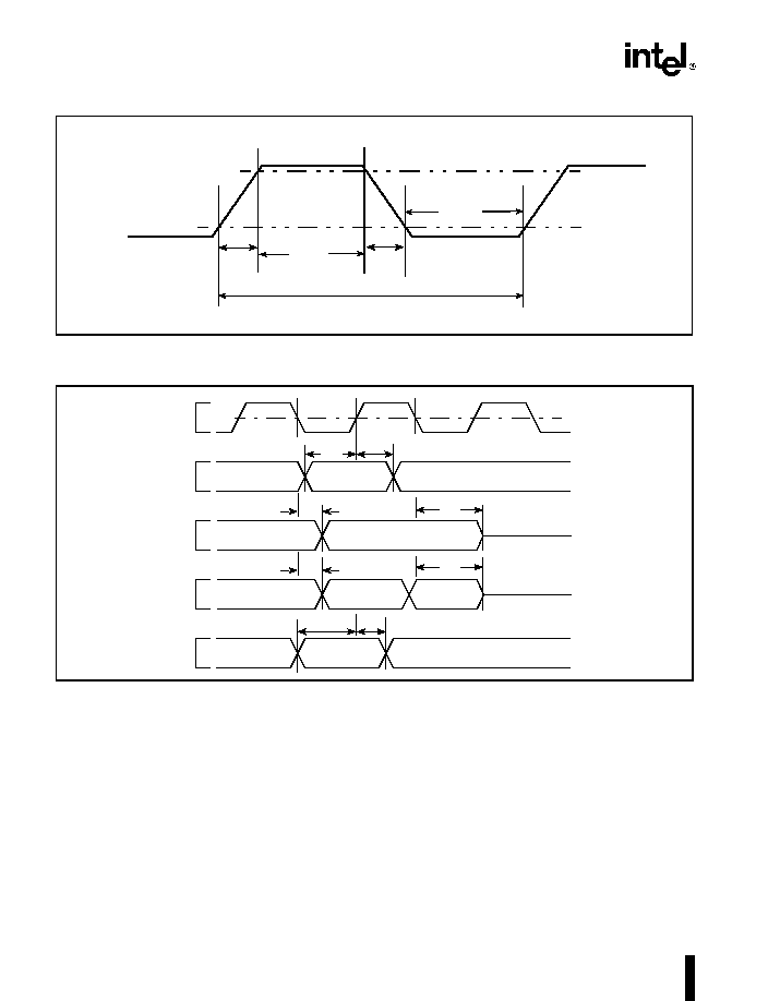
Embedded Ultra-Low Power Intel486TM GX Processor
40
Figure 15. TCK Waveform
Figure 16. Test Signal Timing Diagram
0.8 V
t
26
t25
2.0 V
TCK
t
27
t
28
t
29
0.8 V
2.0 V
t
31
t
30
TCK
TMS
TDI
TDO
OUTPUT
INPUT
VALID
t
32
t
33
VALID
t
35
VALID
VALID
VALID
t
34
t
37
t
36
1.5 V
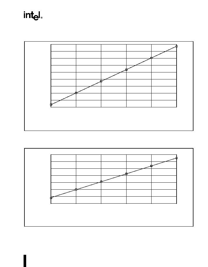
Embedded Ultra-Low Power Intel486TM GX Processor
41
5.4
Capacitive Derating Curves
The following graphs are the capacitive derating curves for the embedded ULP Intel486 GX processor.
Figure 17. Typical Loading Delay versus Load Capacitance under Worst-Case Conditions for a Low-to-
High Transition
Figure 18. Typical Loading Delay versus Load Capacitance under Worst-Case Conditions for a High-
to-Low Transition
nom+7
nom+6
nom+5
nom+4
nom+3
nom+2
nom+1
nom
nom-1
nom-2
25
50
75
100
125
150
Capacitive Load (pF)
Del
ay (ns)
NOTE: This graph will not be linear outside of the capacitive range shown.
nom = nominal value from the AC Characteristics table.
nom+5
nom+4
nom+3
nom+2
nom+1
nom
nom-1
nom-2
25
50
75
100
125
150
Capacitive Load (pF)
Delay (ns)
NOTE: This graph will not be linear outside of the capacitive range shown.
nom = nominal value from the AC Characteristics table.
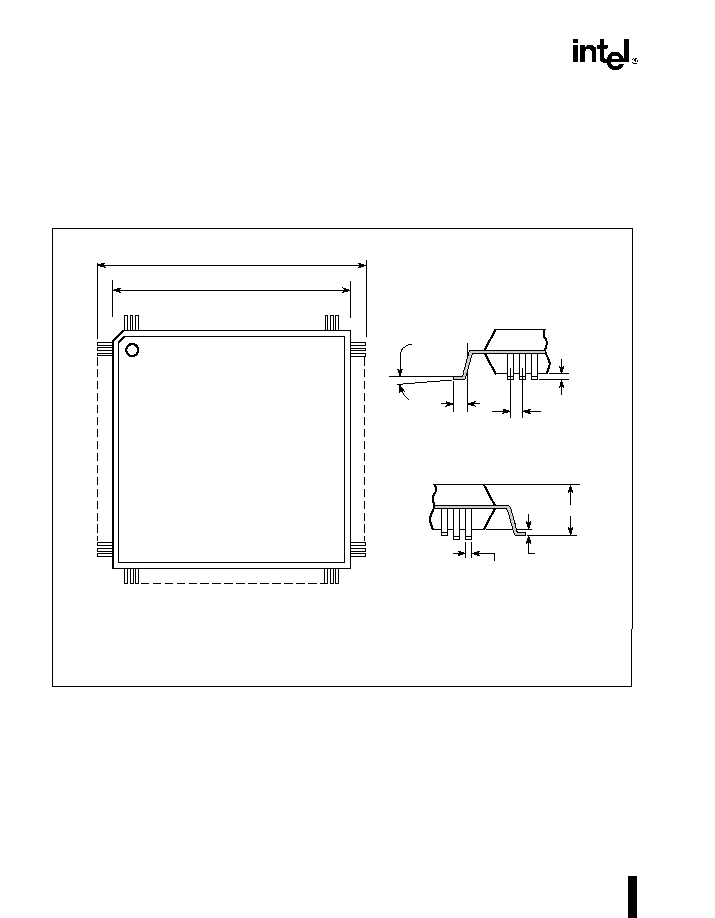
Embedded Ultra-Low Power Intel486TM GX Processor
42
6.0
MECHANICAL DATA
This section describes the packaging dimensions and thermal specifications for the embedded ULP Intel486
GX processor.
6.1
Package Dimensions
Figure 19. Package Mechanical Specifications for the 176-Lead TQFP Package
176
133
45
132
0.10 Ī 0.10
0
į
Min
10
į
Max
0.50 Ī 0.10
0.10 Ī 0.10
1.50 Ī 0.20
0.16 Min
o.28 Max
0.60 Ī 0.20
24.0 Ī 0.10
26.0 Ī 0.40
1
44
88
89
NOTES:
Height measurements same as width measurements
Units: mm
A4586-01
43
Embedded Ultra-Low Power Intel486TM GX Processor
6.2
Package Thermal Specifications
The embedded ULP Intel486 GX processor is
specified for operation when the case temperature
(T
C
) is within the range of 0įC to 85įC. T
C
may be
measured in any environment to determine whether
the processor is within the specified operating range.
The ambient temperature (T
A
) can be calculated
from
JC
and
JA
from the following equations:
T
J
= T
C
+ P *
JC
T
A
= T
J
- P *
JA
T
C
= T
A
+ P * [
JA
-
JC
]
T
A
= T
C
- P * [
JA
-
JC
]
Where T
J
, T
A
, T
C
equals Junction, Ambient and
Case Temperature respectively.
JC
,
JA
equals
Junction-to-Case and Junction-to-Ambient thermal
Resistance, respectively. Maximum Power
Consumption (P) is defined as
P = V (typ) * I
CC
(max)
P = [V
CC
(typ) * I
CC1
(max)] +
[V
CCP
(typ) * I
CC2
(max)]
where:
I
CC1
is the V
CC
supply current
I
CC2
is the V
CCP
supply current
Values for
JA
and
JC
are given in the following
tables for each product at its maximum operating
frequencies.
The following table shows maximum ambient temperatures of the embedded ULP Intel486 GX processor for
each product and maximum operating frequencies. These temperatures are calculated using I
CC1
and I
CC2
values measured during component-validation testing using V
CCP
=3.6 V and worst-case V
CC
values.
Table 21. Thermal Resistance
(įC/W)
JC
and
JA
for the 176-Lead TQFP Package
JC
(įC/W)
JA
(įC/W) with no airflow
4.3
33.6
Table 22. Maximum Ambient Temperature (T
A
)
176-Lead TQFP Package
Frequency
V
CC
T
A
(įC) with no airflow
16 MHz
2.0 V
83
3.3 V
73
20 MHz
2.2 V
80
3.3 V
70
25 MHz
2.4 V
77
3.3 V
66
33 MHz
2.7 V
70
3.3 V
60
