Untitled Document
Intel
®
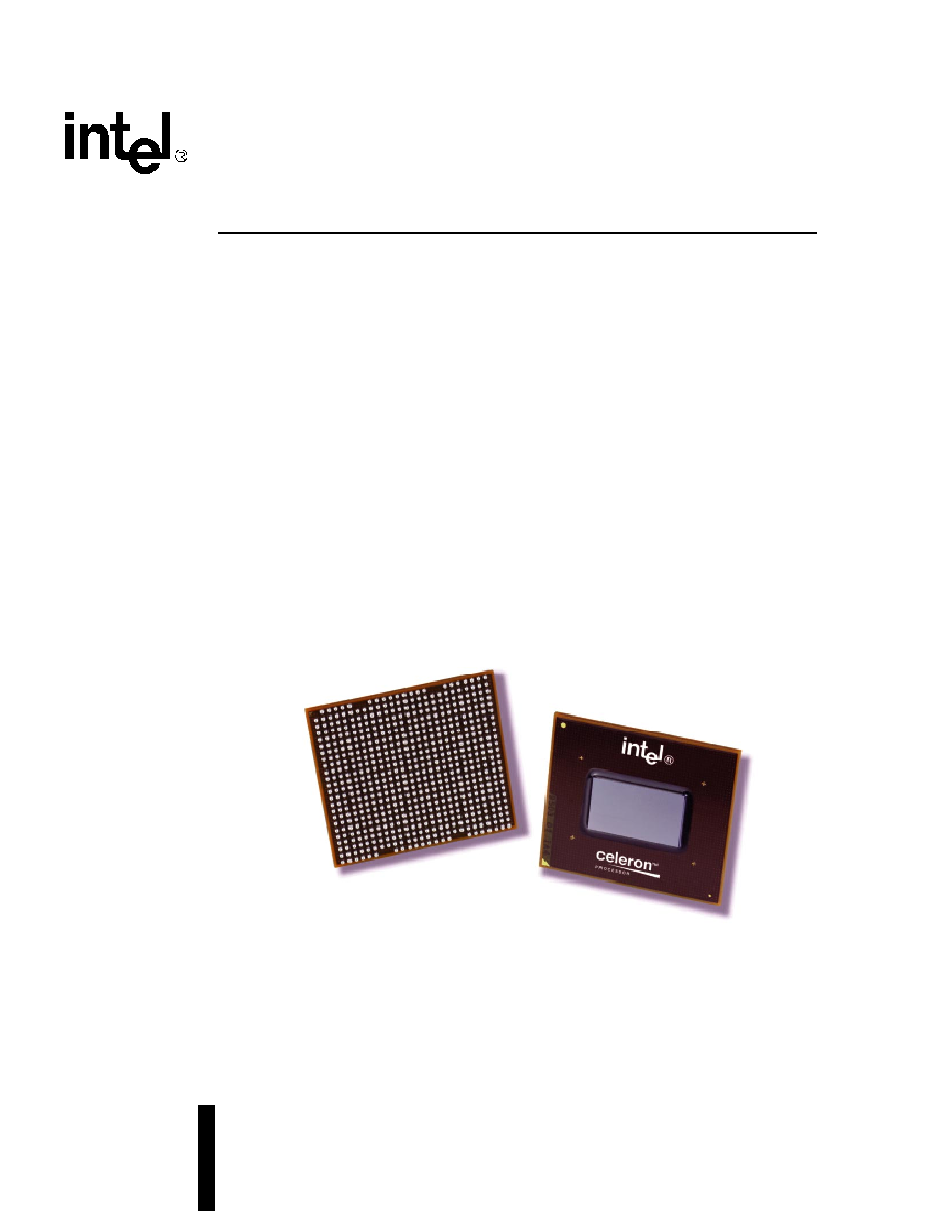
Celeron
®
Processor
Low Power/Ultra Low Power
300 MHz (ULP) and 400A MHz (LP) Processor in a BGA2 Package
Datasheet
Product Features
s
300/100 MHz processor core/bus
speed at 1.1 V (Ultra Low Power)
s
400A/100 MHz processor core/bus
speed at 1.35 V (Low Power)
s
Supports the Intel Architecture with
Dynamic Execution
s
On-die primary 16-Kbyte instruction cache
and 16-Kbyte write-back data cache
s
On-die second level cache (128-Kbyte)
s
Integrated GTL+ termination
s
On-die thermal diode
s
Integrated math co-processor
s
Power Management Features
-- Quick Start and Deep Sleep modes
provide low-power dissipation
s
Fully compatible with previous Intel
microprocessors
-- Binary compatible with all applications
-- Support for MMXTM technology
-- Support for Streaming SIMD Extensions
s
BGA2 packaging technology
-- Supports thin form factor designs
-- Exposed die enables efficient heat
dissipation
Document Number: 273509-001
October 2001

2
Datasheet
Information in this document is provided in connection with Intel
®
products. No license, express or implied, by estoppel or otherwise, to any intellectual
property rights is granted by this document. Except as provided in Intel's Terms and Conditions of Sale for such products, Intel assumes no liability
whatsoever, and Intel disclaims any express or implied warranty, relating to sale and/or use of Intel products including liability or warranties relating to
fitness for a particular purpose, merchantability, or infringement of any patent, copyright or other intellectual property right. Intel products are not
intended for use in medical, life saving, or life sustaining applications.
Intel may make changes to specifications and product descriptions at any time, without notice.
Designers must not rely on the absence or characteristics of any features or instructions marked "reserved" or "undefined." Intel reserves these for
future definition and shall have no responsibility whatsoever for conflicts or incompatibilities arising from future changes to them.
The Intel
®
Celeron
®
Processor Low Power and Intel
®
Celeron
®
Processor Ultra Low Power may contain design defects or errors known as errata
which may cause the product to deviate from published specifications. Current characterized errata are available on request.
MPEG is an international standard for video compression/decompression promoted by ISO. Implementations of MPEG CODECs, or MPEG enabled
platforms may require licenses from various entities, including Intel Corporation.
Contact your local Intel sales office or your distributor to obtain the latest specifications and before placing your product order.
Copies of documents which have an ordering number and are referenced in this document, or other Intel literature may be obtained by calling
1-800-548-4725 or by visiting Intel's website at http://www.intel.com.
Copyright © Intel Corporation, 2001
AlertVIEW, i960, AnyPoint, AppChoice, BoardWatch, BunnyPeople, CablePort, Celeron, Chips, Commerce Cart, CT Connect, CT Media, Dialogic,
DM3, EtherExpress, ETOX, FlashFile, GatherRound, i386, i486, iCat, iCOMP, Insight960, InstantIP, Intel, Intel logo, Intel386, I ntel486, Intel740,
IntelDX2, IntelDX4, IntelSX2, Intel ChatPad, Intel Create&Share, Intel Dot.Station, Intel GigaBlade, Intel InBusiness, Intel Inside, Intel Inside logo, Intel
NetBurst, Intel NetStructure, Intel Play, Intel Play logo, Intel Pocket Concert, Intel SingleDriver, Intel SpeedStep, Intel StrataFlash, Intel TeamStation,
Intel WebOutfitter, Intel Xeon, Intel XScale, Itanium, JobAnalyst, LANDesk, LanRover, MCS, MMX, MMX logo, NetPort, NetportExpress, Optimizer
logo, OverDrive, Paragon, PC Dads, PC Parents, Pentium, Pentium II Xeon, Pentium III Xeon, Performance at Your Command, ProShare,
RemoteExpress, Screamline, Shiva, SmartDie, Solutions960, Sound Mark, StorageExpress, The Computer Inside, The Journey Inside, This Way In,
TokenExpress, Trillium, Vivonic, and VTune are trademarks or registered trademarks of Intel Corporation or its subsidiaries in the United States and
other countries.
*Other names and brands may be claimed as the property of others.

Datasheet
3
Intel
®
Celeron
®
Processor LP/ULP
Contents
1.0
Introduction.................................................................................................................................... 9
1.1
Overview ............................................................................................................................. 10
1.2
Terminology ........................................................................................................................ 10
1.3
References .........................................................................................................................11
2.0
Intel
®
Celeron
®
Processor LP/ULP Features ......................................................................... 11
2.1
Features in the Intel
®
Celeron
®
Processor LP/ULP ......................................................... 11
2.1.1
On-die GTL+ Termination ...................................................................................... 11
2.1.2
Streaming SIMD Extensions ..................................................................................11
2.2
Power Management............................................................................................................ 12
2.2.1
Clock Control Architecture ..................................................................................... 12
2.2.2
Normal State .......................................................................................................... 12
2.2.3
Auto Halt State....................................................................................................... 12
2.2.4
Stop Grant State .................................................................................................... 13
2.2.5
Quick Start State.................................................................................................... 14
2.2.6
HALT/Grant Snoop State ....................................................................................... 14
2.2.7
Sleep State ............................................................................................................14
2.2.8
Deep Sleep State................................................................................................... 15
2.2.9
Operating System Implications of Low-power States ............................................15
2.2.10 GTL+ Signals ......................................................................................................... 15
2.2.11 Intel
®
Celeron
®
Processor LP/ULP CPUID......................................................... 16
3.0
Electrical Specifications ............................................................................................................. 17
3.1
Processor System Signals .................................................................................................. 17
3.1.1
Power Sequencing Requirements ......................................................................... 18
3.1.2
Test Access Port (TAP) Connection ...................................................................... 18
3.1.3
Catastrophic Thermal Protection ........................................................................... 19
3.1.4
Unused Signals......................................................................................................19
3.1.5
Signal State in Low-power States .......................................................................... 19
3.1.5.1
System Bus Signals ............................................................................... 19
3.1.5.2
CMOS and Open-drain Signals ............................................................. 19
3.1.5.3
Other Signals .........................................................................................20
3.2
Power Supply Requirements .............................................................................................. 20
3.2.1
Decoupling Recommendations .............................................................................. 20
3.2.2
Voltage Planes....................................................................................................... 20
3.3
System Bus Clock and Processor Clocking........................................................................ 21
3.4
Maximum Ratings ............................................................................................................... 21
3.5
DC Specifications ............................................................................................................... 23
3.6
AC Specifications................................................................................................................ 26
3.6.1
System Bus, Clock, APIC, TAP, CMOS, and Open-drain AC Specifications ........ 26
4.0
System Signal Simulations......................................................................................................... 35
4.1
System Bus Clock (BCLK) and PICCLK AC Signal Quality Specifications ........................35
4.2
GTL+ AC Signal Quality Specifications .............................................................................. 36
4.3
Non-GTL+ Signal Quality Specifications............................................................................. 40
4.3.1
PWRGOOD Signal Quality Specifications ............................................................. 40

Intel
®
Celeron
®
Processor LP/ULP
4
Datasheet
5.0
Mechanical Specifications.......................................................................................................... 41
5.1
Surface-mount BGA2 Package Dimensions....................................................................... 41
5.2
Signal Listings..................................................................................................................... 43
6.0
Thermal Specifications ............................................................................................................... 51
6.1
Thermal Diode .................................................................................................................... 52
7.0
Processor Initialization and Configuration ............................................................................... 53
7.1
Description.......................................................................................................................... 53
7.1.1
Quick Start Enable................................................................................................. 53
7.1.2
System Bus Frequency.......................................................................................... 53
7.1.3
APIC Enable .......................................................................................................... 53
7.2
Clock Frequencies and Ratios............................................................................................ 53
8.0
Processor Interface ..................................................................................................................... 54
8.1
Alphabetical Signal Reference............................................................................................ 54
8.1.1
A[35:3]# (I/O - GTL+) ............................................................................................. 54
8.1.2
A20M# (I - 1.5 V Tolerant) ..................................................................................... 54
8.1.3
ADS# (I/O - GTL+) ................................................................................................. 54
8.1.4
AERR# (I/O - GTL+) .............................................................................................. 54
8.1.5
AP[1:0]# (I/O - GTL+) ............................................................................................ 54
8.1.6
BCLK (I - 2.5 V Tolerant) ....................................................................................... 55
8.1.7
BERR# (I/O - GTL+) .............................................................................................. 55
8.1.8
BINIT# (I/O - GTL+) ............................................................................................... 55
8.1.9
BNR# (I/O - GTL+)................................................................................................. 55
8.1.10 BP[3:2]# (I/O - GTL+) ............................................................................................ 56
8.1.11 BPM[1:0]# (I/O - GTL+) ......................................................................................... 56
8.1.12 BPRI# (I - GTL+).................................................................................................... 56
8.1.13 BREQ0# (I/O - GTL+) ............................................................................................ 56
8.1.14 BSEL[1:0] (I 3.3 V Tolerant)................................................................................ 56
8.1.15 CLKREF (Analog) .................................................................................................. 56
8.1.16 CMOSREF (Analog) .............................................................................................. 57
8.1.17 D[63:0]# (I/O - GTL+)............................................................................................. 57
8.1.18 DBSY# (I/O - GTL+) .............................................................................................. 57
8.1.19 DEFER# (I - GTL+) ................................................................................................ 57
8.1.20 DEP[7:0]# (I/O - GTL+) .......................................................................................... 57
8.1.21 DRDY# (I/O - GTL+) .............................................................................................. 57
8.1.22 EDGCTRLP (Analog)............................................................................................. 57
8.1.23 FERR# (O - 1.5 V Tolerant Open-drain) ................................................................ 58
8.1.24 FLUSH# (I - 1.5 V Tolerant)................................................................................... 58
8.1.25 HIT# (I/O - GTL+), HITM# (I/O - GTL+) ................................................................. 58
8.1.26 IERR# (O - 1.5 V Tolerant Open-drain) ................................................................. 58
8.1.27 IGNNE# (I - 1.5 V Tolerant) ................................................................................... 58
8.1.28 INIT# (I - 1.5 V Tolerant)........................................................................................ 58
8.1.29 INTR (I - 1.5 V Tolerant) ........................................................................................ 59
8.1.30 LINT[1:0] (I - 1.5 V Tolerant).................................................................................. 59
8.1.31 LOCK# (I/O - GTL+) .............................................................................................. 59
8.1.32 NMI (I - 1.5 V Tolerant) .......................................................................................... 59
8.1.33 PICCLK (I - 2.5 V Tolerant).................................................................................... 59
8.1.34 PICD[1:0] (I/O - 1.5 V Tolerant Open-drain) .......................................................... 60

Datasheet
5
Intel
®
Celeron
®
Processor LP/ULP
8.1.35 PLL1, PLL2 (Analog) ............................................................................................. 60
8.1.36 PRDY# (O - GTL+) ................................................................................................ 60
8.1.37 PREQ# (I - 1.5 V Tolerant) .................................................................................... 60
8.1.38 PWRGOOD (I - 2.5 V Tolerant) ............................................................................. 60
8.1.39 REQ[4:0]# (I/O - GTL+).......................................................................................... 61
8.1.40 RESET# (I - GTL+) ................................................................................................ 61
8.1.41 RP# (I/O - GTL+) ................................................................................................... 61
8.1.42 RS[2:0]# (I - GTL+) ................................................................................................ 61
8.1.43 RSP# (I - GTL+)..................................................................................................... 61
8.1.44 RSVD (TBD) .......................................................................................................... 62
8.1.45 RTTIMPEDP (Analog) ........................................................................................... 62
8.1.46 SLP# (I - 1.5 V Tolerant) ........................................................................................ 62
8.1.47 SMI# (I - 1.5 V Tolerant) ........................................................................................ 62
8.1.48 STPCLK# (I - 1.5 V Tolerant)................................................................................. 62
8.1.49 TCK (I - 1.5 V Tolerant) .........................................................................................62
8.1.50 TDI (I - 1.5 V Tolerant) ........................................................................................... 62
8.1.51 TDO (O - 1.5 V Tolerant Open-drain) .................................................................... 63
8.1.52 TESTHI (I - 1.5 V Tolerant) .................................................................................... 63
8.1.53 TESTLO[2:1] (I - 1.5 V Tolerant)............................................................................63
8.1.54 THERMDA, THERMDC (Analog)........................................................................... 63
8.1.55 TMS (I - 1.5 V Tolerant) .........................................................................................63
8.1.56 TRDY# (I - GTL+) .................................................................................................. 63
8.1.57 TRST# (I - 1.5 V Tolerant) ..................................................................................... 63
8.1.58 VID[4:0] (O Open-drain)...................................................................................... 63
8.1.59 VREF (Analog)....................................................................................................... 64
8.2
Signal Summaries............................................................................................................... 65
9.0
PLL RLC Filter Specification ......................................................................................................67
9.1
Introduction .........................................................................................................................67
9.2
Filter Specification .............................................................................................................. 67
9.3
Recommendation for Low Power Systems ......................................................................... 69
9.4
Comments .......................................................................................................................... 70
Document Outline