Intel(R) Celeron(R) Processor on the 0.13 Micron Process in the 478-Pin Package Datasheet
Intel
®
Celeron
®
Processor on
0.13 Micron Process in the
478-Pin Package
Datasheet
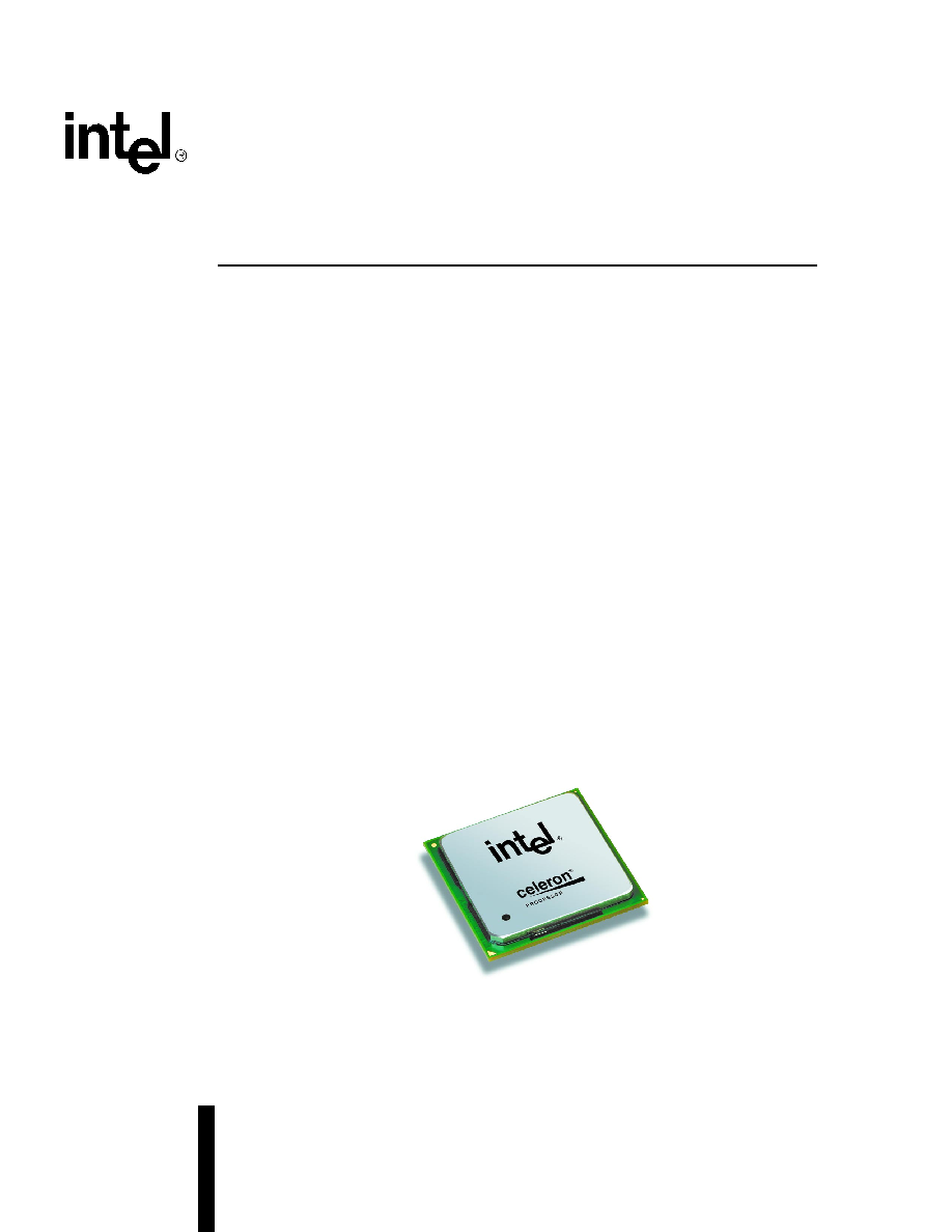
The Intel
®
Celeron
®
processor on 0.13 micron process in the 478-pin package expands Intel's
processor family into the value-priced PC market segment. Celeron processors provide the value
customer the capability to get onto the Internet affordably, and utilize educational programs,
home-office software and productivity applications. All of the Celeron processors include an
integrated L2 cache, and are built on Intel's advanced CMOS process technology. The Celeron
processor is backed by over 30 years of Intel experience in manufacturing high-quality, reliable
microprocessors.
I
Available at 2 GHz, 2.10 GHz, 2.20 GHz,
2.30 GHz, 2.40 GHz, 2.50 MHz, and
2.60 MHz
I
Binary compatible with applications
running on previous members of the Intel
microprocessor line
I
System bus frequency at 400 MHz
I
Rapid Execution Engine: Arithmetic Logic
Units (ALUs) run at twice the processor
core frequency
I
Hyper Pipelined Technology
I
Advanced Dynamic Execution
--Very deep out-of-order execution
--Enhanced branch prediction
I
8-KB Level 1 data cache
I
Level 1 Execution Trace Cache stores 12K
micro-ops and removes decoder latency
from main execution loops
I
128-KB Advanced Transfer Cache (on-die,
full speed Level 2 (L2) cache) with
Error
Correction Code (ECC)
I
144 Streaming SIMD Extensions 2 (SSE2)
Instructions
I
Power Management capabilities
--System Management mode
--Multiple low-power states
I
Optimized for 32-bit applications running
on advanced 32-bit operating systems
June 2003
Document Number: 251748-004

2
Datasheet
INFORMATION IN THIS DOCUMENT IS PROVIDED IN CONNECTION WITH INTEL® PRODUCTS. NO LICENSE, EXPRESS OR IMPLIED, BY
ESTOPPEL OR OTHERWISE, TO ANY INTELLECTUAL PROPERTY RIGHTS IS GRANTED BY THIS DOCUMENT. EXCEPT AS PROVIDED IN
INTEL'S TERMS AND CONDITIONS OF SALE FOR SUCH PRODUCTS, INTEL ASSUMES NO LIABILITY WHATSOEVER, AND INTEL DISCLAIMS
ANY EXPRESS OR IMPLIED WARRANTY, RELATING TO SALE AND/OR USE OF INTEL PRODUCTS INCLUDING LIABILITY OR WARRANTIES
RELATING TO FITNESS FOR A PARTICULAR PURPOSE, MERCHANTABILITY, OR INFRINGEMENT OF ANY PATENT, COPYRIGHT OR OTHER
INTELLECTUAL PROPERTY RIGHT. Intel products are not intended for use in medical, life saving, or life sustaining applications.
Intel may make changes to specifications and product descriptions at any time, without notice.
Designers must not rely on the absence or characteristics of any features or instructions marked "reserved" or "undefined." Intel reserves these for
future definition and shall have no responsibility whatsoever for conflicts or incompatibilities arising from future changes to them.
The Intel
®
Celeron
®
processor may contain design defects or errors known as errata which may cause the product to deviate from published
specifications. Current characterized errata are available on request.
Contact your local Intel sales office or your distributor to obtain the latest specifications and before placing your product order.
Intel, Celeron, Pentium,
and the Intel logo are trademarks or registered trademarks of Intel Corporation or its subsidiaries in the United States and
other countries.
*Other names and brands may be claimed as the property of others.
Copyright © 20022003, Intel Corporation

Datasheet
3
Contents
1.0
Introduction
..................................................................................................................9
1.1
Terminology...........................................................................................................9
1.1.1
Processor Packaging Terminology.........................................................10
1.2
References ..........................................................................................................11
2.0
Electrical Specifications
........................................................................................13
2.1
System Bus and GTLREF ...................................................................................13
2.2
Power and Ground Pins ......................................................................................13
2.3
Decoupling Guidelines ........................................................................................13
2.3.1
VCC
Decoupling .....................................................................................14
2.3.2
System Bus AGTL+ Decoupling.............................................................14
2.3.3
System Bus Clock (BCLK[1:0]) and Processor Clocking .......................14
2.4
Voltage Identification ...........................................................................................15
2.4.1
Phase Lock Loop (PLL) Power and Filter...............................................16
2.5
Reserved, Unused Pins, and TESTHI[12:0]........................................................18
2.6
System Bus Signal Groups .................................................................................19
2.7
Asynchronous GTL+ Signals...............................................................................20
2.8
Test Access Port (TAP) Connection....................................................................20
2.9
System Bus Frequency Select Signals (BSEL[1:0])............................................20
2.10
Maximum Ratings................................................................................................21
2.11
Processor DC Specifications...............................................................................21
2.11.1 Flexible Motherboard Guidelines (FMB).................................................22
2.12
AGTL+ System Bus Specifications .....................................................................28
2.13
System Bus AC Specifications ............................................................................29
2.14
Processor AC Timing Waveforms .......................................................................32
3.0
System Bus Signal Quality Specifications
....................................................41
3.1
System Bus Clock (BCLK) Signal Quality Specifications ....................................41
3.2
System Bus Signal Quality Specifications and Measurement Guidelines...........42
3.3
System Bus Signal Quality Specifications and Measurement Guidelines...........45
3.3.1
Overshoot/Undershoot Guidelines .........................................................45
3.3.2
Overshoot/Undershoot Magnitude .........................................................45
3.3.3
Overshoot/Undershoot Pulse Duration...................................................45
3.3.4
Activity Factor.........................................................................................46
3.3.5
Reading Overshoot/Undershoot Specification Tables............................46
3.3.6
Conformance Determination to Overshoot/Undershoot
Specifications .........................................................................................47
4.0
Package Mechanical Specifications
.................................................................51
4.1
Package Load Specifications ..............................................................................54
4.2
Processor Insertion Specifications ......................................................................55
4.3
Processor Mass Specifications ...........................................................................55
4.4
Processor Materials.............................................................................................55
4.5
Processor Markings.............................................................................................55
5.0
Pin Listing and Signal Definitions
.....................................................................59
5.1
Processor Pin Assignments ................................................................................59

4
Datasheet
5.2
Alphabetical Signals Reference .......................................................................... 72
6.0
Thermal Specifications and Design Considerations
................................. 81
6.1
Processor Thermal Specifications....................................................................... 82
6.1.1
Thermal Specifications........................................................................... 82
6.1.2
Thermal Metrology ................................................................................. 83
6.1.2.1 Processor Case Temperature Measurement ............................ 83
7.0
Features
....................................................................................................................... 85
7.1
Power-On Configuration Options ........................................................................ 85
7.2
Clock Control and Low Power States.................................................................. 85
7.2.1
Normal State--State 1 ........................................................................... 85
7.2.2
AutoHALT Powerdown State--State 2 .................................................. 86
7.2.3
Stop-Grant State--State 3 ..................................................................... 87
7.2.4
HALT/Grant Snoop State--State 4 ........................................................ 87
7.2.5
Sleep State--State 5.............................................................................. 88
7.3
Thermal Monitor .................................................................................................. 88
7.3.1
Thermal Diode........................................................................................ 90
8.0
Boxed Processor Specifications
....................................................................... 91
8.1
Introduction ......................................................................................................... 91
8.2
Mechanical Specifications................................................................................... 92
8.2.1
Boxed Processor Cooling Solution Dimensions..................................... 92
8.2.2
Boxed Processor Fan Heatsink Weight.................................................. 93
8.2.3
Boxed Processor Retention Mechanism and Heatsink Assembly.......... 93
8.3
Electrical Requirements ...................................................................................... 94
8.3.1
Fan Heatsink Power Supply................................................................... 94
8.4
Thermal Specifications........................................................................................ 96
8.4.1
Boxed Processor Cooling Requirements ............................................... 96
8.4.2
Variable Speed Fan ............................................................................... 97
9.0
Debug Tools Specifications
................................................................................. 99
9.1
Logic Analyzer Interface (LAI)............................................................................. 99
9.1.1
Mechanical Considerations .................................................................... 99
9.1.2
Electrical Considerations........................................................................ 99

Datasheet
5
Figures
1
VCCVID Pin Voltage and Current Requirements ................................................15
2
Typical VCCIOPLL, VCCA and VSSA Power Distribution ..................................17
3
Phase Lock Loop (PLL) Filter Requirements ......................................................17
4
VCC Static and Transient Tolerance...................................................................24
5
ITPCLKOUT[1:0] Output Buffer Diagram ............................................................27
6
AC Test Circuit ....................................................................................................32
7
TCK Clock Waveform..........................................................................................33
8
Differential Clock Waveform................................................................................33
9
Differential Clock Crosspoint Specification..........................................................34
10
System Bus Common Clock Valid Delay Timings...............................................34
11
System Bus Reset and Configuration Timings....................................................35
12
Source Synchronous 2X (Address) Timings .......................................................35
13
Source Synchronous 4X Timings ........................................................................36
14
Power Up Sequence ...........................................................................................37
15
Power Down Sequence.......................................................................................37
16
Test Reset Timings .............................................................................................38
17
THERMTRIP# Power Down Sequence...............................................................38
18
ITPCLKOUT Valid Delay Timing .........................................................................38
19
FERR#/PBE# Valid Delay Timing .......................................................................39
20
TAP Valid Delay Timing ......................................................................................39
21
BCLK Signal Integrity Waveform.........................................................................41
22
Low-to-High System Bus Receiver Ringback Tolerance.....................................43
23
High-to-Low System Bus Receiver Ringback Tolerance.....................................43
24
Low-to-High System Bus Receiver Ringback Tolerance for PWRGOOD
and TAP Buffers ..................................................................................................44
25
High-to-Low System Bus Receiver Ringback Tolerance for PWRGOOD
and TAP Buffers ..................................................................................................44
26
Maximum Acceptable Overshoot/Undershoot Waveform ...................................49
27
Exploded View of Processor Components on a System Board ..........................51
28
Processor Package .............................................................................................52
29
Processor Cross-Section and Keep-In ................................................................53
30
Processor Pin Detail............................................................................................53
31
IHS Flatness Specification ..................................................................................54
32
Processor Markings.............................................................................................55
33
Processor Pinout Coordinates (Top View, Left Side) ..........................................56
34
Processor Pinout Coordinates (Top View, Right Side)........................................57
35
Example Thermal Solution (Not to Scale) ...........................................................81
36
Guideline Locations for Case Temperature (TC) Thermocouple Placement ......83
37
Stop Clock State Machine ...................................................................................86
38
Mechanical Representation of the Boxed Processor ..........................................91
39
Side View Space Requirements for the Boxed Processor ..................................92
40
Top View Space Requirements for the Boxed Processor ...................................93
41
Boxed Processor Fan Heatsink Power Cable Connector Description.................94
42
MotherBoard Power Header Placement Relative to Processor Socket ..............95
43
Boxed Processor Fan Heatsink Airspace Keep-Out Requirements
(Side 1 View) .......................................................................................................96
44
Boxed Processor Fan Heatsink Airspace Keep-Out Requirements
(Side 2 View) .......................................................................................................97
45
Boxed Processor Fan Heatsink Set Points .........................................................97
Document Outline