
November 1991
Order Number 271077-006
M82C288
BUS CONTROLLER FOR M80286 PROCESSORS
(M82C288-10 M82C288-8 M82C288-6)
Military
Y
Provides Commands and Controls for
Local and System Bus
Y
Wide Flexibility in System
Configurations
Y
Implemented in High Speed CHMOS III
Technology
Y
Fully Compatible with the HMOS
M82288
Y
Fully Static Device
Y
Single
a
5V Supply
Y
Available in 20 Pin Cerdip Package
(See Packaging Spec Order
231369)
The Intel M82C288 Bus Controller is a 20-pin CHMOS III component for use in M80C286 microsystems The
M82C288 is fully compatible with its predecessor the HMOS M82288 The bus controller is fully static and
supports a low power mode The bus controller provides command and control outputs with flexible timing
options Separate command outputs are used for memory and I O devices The data bus is controlled with
separate data enable and direction control signals
Two modes of operation are possible via a strapping option MULTIBUS Compatible bus cycles and high
speed bus cycles
271077 ≠ 1
Figure 1 M82C288 Block Diagram
20 Pin Cerdip Package
271077 ≠ 2
Figure 2 M82C288 Pin
Configuration

M82C288
Table 1 Pin Description
The following pin function descriptions are for the M82C288 bus controller
Symbol Type
Name and Function
CLK
I
SYSTEM CLOCK
provides the basic timing control for the M82C288 in an M80286
microsystem Its frequency is twice the internal processor clock frequency The falling edge
of this input signal establishes when inputs are sampled and command and control outputs
change
S0 S1
I
BUS CYCLE STATUS
starts a bus cycle and along with M IO defines the type of bus
cycle These inputs are active LOW A bus cycle is started when either S1 or S0 is sampled
LOW at the falling edge of CLK Setup and hold times must be met for proper operation
M80286 Bus Cycle Status Definition
M IO
S1
S0
Type of Bus Cycle
0
0
0
Interrupt Acknowledge
0
0
1
I O Read
0
1
0
I O Write
0
1
1
None Idle
1
0
0
Halt or Shutdown
1
0
1
Memory Read
1
1
0
Memory Write
1
1
1
None Idle
M IO
I
MEMORY OR I O SELECT
determines whether the current bus cycle is in the memory
space or I O space When LOW the current bus cycle is in the I O space Setup and hold
times must be met for proper operation
MB
I
MULTIBUS MODE SELECT
determines timing of the command and control outputs When
HIGH the bus controller operates with MULTIBUS I compatible timings When LOW the
bus controller optimizes the command and control output timing for short bus cycles The
function of the CEN AEN input pin is selected by this signal This input is typically a
strapping option and not dynamically changed
CENL
I
COMMAND ENABLE LATCHED
is a bus controller select signal which enables the bus
controller to resopnd to the current bus cycle being initiated CENL is an active HIGH input
latched internally at the end of each T
S
cycle CENL is used to select the appropriate bus
controller for each bus cycle in a system where the CPU has more than one bus it can use
This input may be connected to V
CC
to select this M82C288 for all transfers No control
inputs affect CENL Setup and hold times must be met for proper operation
CMDLY
I
COMMAND DELAY
allows delaying the start of a command CMDLY is an active HIGH
input If sampled HIGH the command output is not activated and CMDLY is again sampled
at the next CLK cycle When sampled LOW the selected command is enabled If READY is
detected LOW before the command output is activated the M82C288 will terminate the bus
cycle even if no command was issued Setup and hold times must be satisified for proper
operation This input may be connected to GND if no delays are required before starting a
command This input has no effect on M82C288 control outputs
READY
I
READY
indicates the end of the current bus cycle READY is an active LOW input
MULTIBUS I mode requires at least one wait state to allow the command outputs to
become active READY must be LOW during reset to force the M82C288 into the idle state
Setup and hold times must be met for proper operation The M82C284 drives READY LOW
during RESET
2

M82C288
Table 1 Pin Description
(Continued)
Symbol
Type
Name and Function
CEN AEN
I
COMMAND ENABLE ADDRESS ENABLE
controls the command and DEN
outputs of the bus controller CEN AEN inputs may be asynchronous to CLK
Setup and hold times are given to assure a guaranteed response to synchronous
inputs This input may be connected to V
CC
or GND
When MB is HIGH this pin has the AEN function AEN is an active LOW input which
indicates that the CPU has been granted use of a shared bus and the bus controller
command outputs may exit 3-state OFF and become inactive (HIGH) AEN HIGH
indicates that the CPU does not have control of the shared bus and forces the
command outputs into 3-state OFF and DEN inactive (LOW)
When MB is LOW this pin has the CEN function CEN is an unlatched active HIGH
input which allows the bus controller to activate its command and DEN outputs
With MB LOW CEN LOW forces the command and DEN outputs inactive but does
not tristate them
ALE
O
ADDRESS LATCH ENABLE
controls the address latches used to hold an address
stable during a bus cycle This control output is active HIGH ALE will not be issued
for the halt bus cycle and is not affected by any of the control inputs
MCE
O
MASTER CASCADE ENABLE
signals that a cascade address from a master
M8259A interrupt controller may be placed onto the CPU address bus for latching
by the address latches under ALE control The CPU's address bus may then be
used to broadcast the cascade address to slave interrupt controllers so only one of
them will respond to the interrupt acknowledge cycle This control output is active
HIGH MCE is only active during interrupt acknowledge cycles and is not affected
by any control input Using MCE to enable cascade address drivers requires
latches which save the cascade address on the falling edge of ALE
DEN
O
DATA ENABLE
controls when data transceivers connected to the local data bus
should be enabled DEN is an active HIGH control output DEN is delayed for write
cycles in the MULTIBUS I mode
DT R
O
DATA TRANSMIT RECEIVE
establishes the direction of data flow to or from the
local data bus When HIGH this control output indicates that a write bus cycle is
being performed A LOW indicates a read bus cycle DEN is always inactive when
DT R changes states This output is HIGH when no bus cycle is active DT R is not
affected by any of the control inputs
IOWC
O
I O WRITE COMMAND
instructs an I O device to read the data on the data bus
This command output is active LOW The MB and CMDLY input control when this
output becomes active READY controls when it becomes inactive
IORC
O
I O READ COMMAND
instructs an I O device to place data onto the data bus
This command output is active LOW The MB and CMDLY input control when this
output becomes active READY controls when it become inactive
MWTC
O
MEMORY WRITE COMMAND
instructs a memory device to read the data on the
data bus This command output is active LOW The MB and CMDLY inputs control
when this output becomes active READY controls when it becomes inactive
MRDC
O
MEMORY READ COMMAND
instructs the memory device to place data onto the
data bus This command output is active LOW The MB and CMDLY inputs control
when this output becomes active READY controls when it becomes inactive
3

M82C288
Table 1 Pin Description
(Continued)
Symbol
Type
Name and Function
INTA
O
INTERRUPT ACKNOWLEDGE
tells an interrupting device that its interrupt request
is being acknowledged This command output is active LOW The MB and CMDLY
inputs control when this output becomes active READY controls when it becomes
inactive
V
CC
System Power a
5V Power Supply
GND
System Ground
0V
Table 2 Command and Control Outputs for Each Type of Bus Cycle
Type of
M IO
S1
S0
Command
DT R
ALE DEN
MCE
Bus Cycle
Activated
State
Issued
Issued
Interrupt Acknowledge
0
0
0
INTA
LOW
YES
YES
I O Read
0
0
1
IORC
LOW
YES
NO
I O Write
0
1
0
IOWC
HIGH
YES
NO
None Idle
0
1
1
None
HIGH
NO
NO
Halt Shutdown
1
0
0
None
HIGH
NO
NO
Memory Read
1
0
1
MRDC
LOW
YES
NO
Memory Write
1
1
0
MWTC
HIGH
YES
NO
None Idle
1
1
1
None
HIGH
NO
NO
Operating Modes
Two types of buses are supported by the M82C288
MULTIBUS I and non-MULTIBUS I When the MB
input is strapped HIGH MULTIBUS I timing is used
In MULTIBUS I mode the M82C288 delays com-
mand and data activation to meet IEEE-796 require-
ments on address to command active and write data
to command active setup timing MULTIBUS I mode
requires at least one wait state in the bus cycle since
the command outputs are delayed
The non-
MULTIBUS I mode does not delay any outputs and
does not require wait states The MB input affects
the timing of the command and DEN outputs
Command and Control Outputs
The type of bus cycle performed by the local bus
master is encoded in the M IO S1 and S0 inputs
Different command and control outputs are activat-
ed depending on the type of bus cycle Table 2 indi-
cates the cycle decode done by the M82C288 and
the effect on command DT R ALE DEN and MCE
outputs
Bus cycles come in three forms read write and
halt Read bus cycles include memory read I O
read and interrupt acknowledge The timing of the
associated read command outputs (MRDC IORC
and INTA) control outputs (ALE DEN DT R) and
control inputs (CEN AEN CENL CMDLY MB and
READY) are identical for all read bus cycles Read
cycles differ only in which command output is acti-
vated The MCE control output is only asserted dur-
ing interrupt acknowledge cycles
Write bus cycles activate different control and com-
mand outputs with different timing than read bus cy-
cles Memory write and I O write are write bus cy-
cles whose timing for command outputs (MWTC and
IOWC) control outputs (ALE DEN DT R) and con-
trol inputs (CEN AEN
CENL
CMDLY
MB and
READY) are identical They differ only in which com-
mand output is activated
Halt bus cycles are different because no command
or control output is activated All control inputs are
ignored until the next bus cycle is started via S1 and
S0
Static Operation
All M82C288 circuitry is of static design Internal reg-
isters and logic are static and require no refresh as
with dynamic circuit design This eliminates the mini-
mum operating frequency restriction placed on the
HMOS M82288 The CHMOS III M82C288 can oper-
ate from DC to the appropriate upper frequency limit
4
M82C288
The clock may be stopped in either state (HIGH
LOW) and held there indefinitely
Power dissipation is directly related to operating fre-
quency As the system frequency is reduced so is
the operating power When the clock is stopped to
the M82C288 power dissipation is at a minimum
This is useful for low-power and portable applica-
tions
FUNCTIONAL DESCRIPTION
Description
The M82C288 bus controller is used in M80286 sys-
tems to provide address latch control data trans-
ceiver control and standard level-type command
outputs The command outputs are timed and have
sufficient drive capabilities for large TTL buses and
meet all IEEE-796 requirements for MULTIBUS I A
special MULTIBUS I mode is provided to satisfy all
address data setup and hold time requirements
Command timing may be tailored to special needs
via a CMDLY input to determine the start of a com-
mand and READY to determine the end of a com-
mand
Connection to multiple buses are supported with a
latched enable input (CENL) An address decoder
can determine which if any bus controller should be
enabled for the bus cycle This input is latched to
allow an address decoder to take full advantage of
the pipelined timing on the M80286 local bus
Buses shared by several bus controllers are sup-
ported An AEN input prevents the bus controller
from driving the shared bus command and data
signals except when enabled by an external MULTI-
BUS I type bus arbiter
Separate DEN and DT R outputs control the data
transceivers for all buses Bus contention is eliminat-
ed by disabling DEN before changing DT R The
DEN timing allows sufficient time for tristate bus driv-
ers to enter 3-state OFF before enabling other driv-
ers onto the same bus
The term CPU refers to any M80286 processor or
M80286 support component which may become an
M80286 local bus master and thereby drive the
M82C288 status inputs
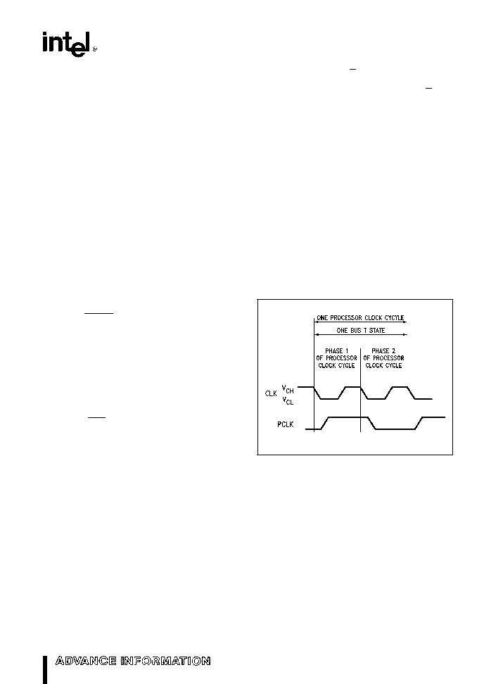
Processor Cycle Definition
Any CPU which drives the local bus uses an internal
clock which is one half the frequency of the system
clock (CLK) (see Figure 3) Knowledge of the phase
of the local bus master internal clock is required for
proper operation of the M80286 local bus The local
bus master informs the bus controller of its internal
clock phase when it asserts the status signals
Status signals are always asserted beginning in
Phase 1 of the local bus master's internal clock
M82C284
271077 ≠ 3
(FOR REFERENCE)
Figure 3 CLK Relationship to the Processor
Clock and Bus T-States
5

M82C288
Bus State Definition
The M82C288 bus controller has three bus states
(see Figure 4) Idle (T
I
) Status (T
S
) and Command
(T
C
) Each bus state is two CLK cycles long Bus
state phases correspond to the internal CPU proces-
sor clock phases
The T
I
bus state occurs when no bus cycle is cur-
rently active on the M80286 local bus This state
may be repeated indefinitely When control of the
local bus is being passed between masters the bus
remains in the T
I
state
271077 ≠ 4
Figure 4 M82C288 Bus States
Bus Cycle Definition
The S1 and S0 inpus signal the start of a bus cycle
When either input becomes LOW a bus cycle is
started The T
S
bus state is defined to be the two
CLK cycles during which either S1 or S0 are active
(see Figure 5) These inputs are sampled by the
M82C288 at every falling edge of CLK When either
S1 and S0 are sampled LOW the next CLK cycle is
considered the second phase of the internal CPU
clock cycle
The local bus enters the T
C
bus state after the T
S
state The shortest bus cycle may have one T
S
state
and one T
C
state Longer bus cycles are formed by
repeating T
C
state A repeated T
C
bus state is called
a wait state
The READY input determines whether the current
T
C
bus state is to be repeated The READY input
has the same timing and effect for all bus cycles
READY is sampled at the end of each T
C
bus state
to see if it is active If sampled HIGH The T
C
bus
state is repeated This is called inserting a wait state
The control and command outputs do not change
during wait states
When READY is sampled LOW the current bus cy-
cle is terminated Note that the bus controller may
enter the T
S
bus state directly from T
C
if the status
lines are sampled active at the next falling edge of
CLK
271077 ≠ 5
Figure 5 Bus Cycle Definition
6

M82C288
Figures 6 through 10 show the basic command and
control output timing for read and write bus cycles
Halt bus cycles are not shown since they activate no
outputs The basic idle-read-idle and idle-write-idle
bus cycles are shown The signal label CMD repre-
sents the appropriate command output for the bus
cycle For Figures 6 through 10 the CMDLY input is
connected to GND and CENL to V
CC
The effects of
CENL and CMDLY are described later in the section
on control inputs
Figures 6 7 and 8 show non-MULTIBUS I cycles
MB is cnonected to GND while CEN is connected to
V
CC
Figure 6 shows a read cycle with no wait states
while Figure 7 shows a write cycle with one wait
state The READY input is shown to illustrate how
wait states are added
271077 ≠ 6
Figure 6 Idle-Read-Idle Bus Cycles with MB e 0
271077 ≠ 7
Figure 7 Idle-Write-Idle Bus Cycles with MB e 0
7

M82C288
Bus cycles can occur back to back with no T
I
bus
states between T
C
and T
S
Back to back cycles do
not affect the timing of the command and control
outputs
Command and control outputs always
reach the states shown for the same clock edge
(within T
S
T
C
or following bus state) of a bus cycle
A special case in control timing occurs for back to
back write cycles with MB e 0 In this case DT R
and DEN remain HIGH between the bus cycles (see
Figure 8) The command and ALE output timing
does not change
Figures 9 and 10 show a MULTIBUS I cycle with MB
e
1 AEN and CMDLY are connected to GND The
effects of CMDLY and AEN are described later in
the section on control inputs Figure 9 shows a read
cycle with one wait state and Figure 10 shows a
write cycle with two waits states The second wait
state of the write cycle is shown only for example
purposes and is not required The READY input is
shown to illustate how wait states are added
271077 ≠ 8
Figure 8 Write-Write Bus Cycles with MB e 0
271077 ≠ 9
Figure 9 Idle-Read-Idle Bus Cycles with 1 Wait State and with MB e 1
8

M82C288
271077 ≠ 10
Figure 10 Idle-Write-Idle Bus Cycles with 2 Wait States and with MB e 1
The MB control input affects the timing of the com-
mand and DEN outputs These outputs are automat-
ically delayed in MULTIBUS I mode to satisfy three
requirements
1) 50 ns minimum setup time for valid address be-
fore any command output becomes active
2) 50 ns minimum setup time for valid write data be-
fore any write command output becomes active
3) 65 ns maximum time from when any read com-
mand becomes inactive until the slave's read
data drivers read 3-state OFF
Three signal transitions are delayed by MB e 1 as
compared to MB e 0
1) The HIGH to LOW transition of the read com-
mand outputs (IORC MRDC and INTA) are de-
layed one CLK cycle
2) The HIGH to LOW transition of the write com-
mand outputs (IOWC nd MWTC) are delayed two
CLK cycles
3) The LOW to HIGH transition of DEN of write cy-
cles is delayed one CLK cycle
Back to back bus cycles with MB e 1 do not change
the timing of any of the command or control outputs
DEN always becomes inactive between bus cycles
with MB e 1
Except for a halt or shutdown bus cycle ALE will be
issued during the second half of T
S
for any bus cy-
cle ALE becomes inactive at the end of the T
S
to
allow latching the address to keep it stable during
the entire bus cycle The address outputs may
change during Phase 2 of any T
C
bus state ALE is
not affected by any control input
Figure 11 shows how MCE is timed during interrupt
acknlwedged (INTA) bus cycles MCE is one CLK
cycle longer than ALE to hold the cascade address
from a master M8259A valid after the falling edge of
ALE With the exception of the MCE control output
an INTA bus cycle is identical in timing to a read bus
cycle MCE is not affected by any control input
9
M82C288
271077 ≠ 11
Figure 11 MCE Operation for an INTA Bus Cycle
Control Inputs
The control inputs can alter the basic timing of com-
mand outputs allow interfacing to multiple buses
and share a bus between different masters For
many M80286 systems each CPU will have more
than one bus which may be used to perform a bus
cycle Normally a CPU will only have one bus con-
troller active for each bus cycle Some buses may be
shared by more than one CPU (i e MULTIBUS) re-
quiring only one of them use the bus at a time
Systems with multiple and shared buses use two
control input signals of the M82C288 bus controller
CENL and AEN (see Figure 12) CENL enables the
bus controller to control the current bus cycle The
AEN input prevents a bus controller from driving its
command outputs AEN HIGH means that another
bus controller may be driving the shared bus
In Figure 12 two buses are shown a local bus and a
MULTIBUS I Only one bus is used for each CPU
bus cycle The CENL inputs of the bus controller
select which bus controller is to perform the bus cy-
cle An address decoder determines which bus to
use for each bus cycle The M82C288 connected to
the shared MULTIBUS I must be selected by CENL
and be given access to the MULTIBUS I by AEN
before it will begin a MULTIBUS I operation
CENL must be sampled HIGH at the end of the T
S
bus state (see waveforms) to enable the bus control-
ler to activate its command and control outputs If
sampled LOW the commands and DEN will not go
active and DT R will remain HIGH The bus control-
ler will ignore the CMDLY CEN and READY inputs
until another bus cycle is started via S1 and S0
Since an address decoder is commonly used to
identify which bus is required for each bus cycle
CENL is latched to avoid the need for latching its
inputs
The CENL input can affect the DEN control output
When MB e 0 DEN normally becomes active dur-
ing Phase 2 of T
S
in write bus cycles This transition
occurs before CENL is sampled If CENL is sampled
LOW the DEN output will be forced LOW during T
C
as shown in the timing waveforms
When MB e 1 CEN AEN becomes AEN AEN con-
trols when the bus controller command outputs en-
ter and exit 3-state OFF AEN is intended to be driv-
en by a MULTIBUS I type bus arbiter which assures
only one bus controller is driving the shared bus at
any time When AEN makes a LOW to HIGH tran-
sition
the command outputs immediately enter
3-state OFF and DEN is forced inactive An inactive
DEN should force the local data transceivers con-
nected to the shared data bus into 3-state OFF (see
Figure 12) The LOW to HIGH transition of AEN
should only occur during T
I
or T
S
bus states
The HIGH to LOW transition of AEN signals that the
bus controller may now drive the shared bus com-
mand signals Since a bus cycle may be active or be
in the process of starting AEN can become active
during any T-state AEN LOW immediately allows
DEN to go the appropriate state Three CLK edges
later the command outputs will go active (see timing
waveforms) The MULTIBUS I requires this delay for
the address and data to be valid on the bus before
the command becomes active
When MB e 0 CEN AEN becomes CEN CEN is an
asynchronous input which immediately affects the
command and DEN outputs When CEN makes a
HIGH to LOW transition the commands and DEN
10
M82C288
are immediately forced inactive When CEN makes a
LOW to HIGH transition the commands and DEN
outputs immediately go to the appropriate state (see
timing waveforms) READY must still become active
to terminate a bus cycle if CEN remains LOW for a
selected bus controller (CENL was latched HIGH)
Some memory or I O systems may require more ad-
dress or write data setup time to command active
than provided by the basic command output timing
To provide flexible command timing the CMDLY in-
put can delay the activation of command outputs
The CMDLY input must be sampled LOW to activate
the command outputs CMDLY does not affect the
control outputs ALE MCE DEN and DT R
271077 ≠ 12
Figure 12 System Use of AEN and CENL
11

M82C288
CMDLY is first sampled on the falling edge of the
CLK ending T
S
If sampled HIGH the command out-
put is not activated and CMDLY is again sampled
on the next falling edge of CLK Once sampled
LOW the proper command output becomes active
immediately if MB e 0 If MB e 1 the proper com-
mand goes active no earlier than shown in Figures 9
and 10
READY can terminate a bus cycle before CMDLY
allows a command to be issued In this case no
commands are issued an the bus controller will de-
activate DEN and DT R in the same manner as if a
command has been issued
Waveforms Discussion
The waveforms show the timing relationships of in-
puts and outputs and do not show all possible tran-
sitions of all signals in all modes Instead all signal
timing relationships are shown via the general cas-
es Special cases are shown when needed The
waveforms provide some functional descriptions of
the M82C288 however most functional descriptions
are provided in Figures 5 through 11
To find the timing specification for a signal transition
in a particular mode first look for a special case in
the waveforms If no special case applies then use
a timing specification for the same or related func-
tion in another mode
12
M82C288
ABSOLUTE MAXIMUM RATINGS
Case Temperature
Under Bias
b
55 C to a125 C
Storage Temperature
b
65 C to a150 C
Voltage on Any Pin with
Respect to GND
b
0 5V to a7V
Power Dissipation
1 Watt
NOTICE This data sheet contains information on
products in the sampling and initial production phases
of development The specifications are subject to
change without notice Verify with your local Intel
Sales office that you have the latest data sheet be-
fore finalizing a design
WARNING Stressing the device beyond the ``Absolute
Maximum Ratings'' may cause permanent damage
These are stress ratings only Operation beyond the
``Operating Conditions'' is not recommended and ex-
tended exposure beyond the ``Operating Conditions''
may affect device reliability
Operating Conditions
Symbol
Description
Min
Max
Unis
T
C
Case Temperature (Instant On)
b
55
a
125
C
V
CC
Digital Supply Voltage
4 75
5 25
V
D C CHARACTERISTICS
(Over Specified Operating Conditions)
Symbol
Parameter
Min
Max
Units
Comments
V
IL
Input LOW Voltage
b
0 5
0 8
V
V
IH
Input HIGH Voltage
2 0
V
CC
a
0 5
V
V
ILC
CLK Input LOW Voltage
b
0 5
0 6
V
V
IHC
CLK Input HIGH Voltage
3 8
V
CC
a
0 5
V
V
OL
Output LOW Voltage
Command Outputs
0 45
V
I
OL
e
32 mA (Note 1)
Control Outputs
0 45
V
I
OL
e
16 mA (Note 2)
V
OH
Output HIGH Voltage
Command Outputs
2 4
V
I
OH
e b
5 mA (Note 1)
V
CC
b
0 5
V
I
OH
e b
1 mA (Note 1)
Control Outputs
2 4
V
I
OH
e b
1 mA (Note 2)
V
CC
b
0 5
V
I
OH
e b
0 2 mA (Note 2)
I
IL
Input Leakage Current
g
10
m
A
0V
s
V
IN
s
V
CC
I
LO
Output Leakage Current
g
10
m
A
0 45V
s
V
OUT
s
V
CC
I
CC
Power Supply Current
75
mA
I
CCS
Power Supply Current (Static)
3
mA
(Note 3)
C
CLK
CLK Input Capacitance
12
pF
F
C
e
1 MHz
C
I
Input Capacitance
10
pF
F
C
e
1 MHz
C
O
Input Outut Capacitance
20
pF
F
C
e
1 MHz
NOTES
1 Commands Outputs are INTA IORC IOWC MRDC and MWRC
2 Control Outputs are DT R DEN ALE and MCE
3 Tested while outputs are unloaded and inputs at V
CC
or V
SS
13

M82C288
A C CHARACTERISTICS
(Over Specified Operating Conditions)
AC timings are referenced to 0 8V and 2 0V points of signals as illustrated in data sheet waveforms unless
otherwise noted
Symbol
Parameter
6 MHz
8 MHz
10 MHz
Unit
Comments
(Advance)
(Advance)
(Advance)
-6
-6
-8
-8
-10
-10
Min
Max
Min
Max
Min
Max
1
CLK Period
83
250
62
250
50
250
ns
2
CLK HIGH Time
25
20
16
ns
at 3 6V
3
CLK LOW Time
20
15
12
ns
at 1 0V
4
CLK Rise Time
10
10
8
ns
1 0V to 3 6V
5
CLK Fall Time
10
10
8
ns
3 6V to 1 0V
6
M IO and Status
28
22
18
ns
Setup Time
7
M IO and Status
1
1
1
ns
Hold Time
8
CENL Setup Time
30
20
15
ns
9
CENL Hold Time
1
1
1
ns
10
READY Setup Time
50
38
26
ns
11
READY Hold Time
35
25
25
ns
12
CMDLY Setup Time
25
20
15
ns
13
CMDLY Hold Time
1
1
1
ns
14
AEN Setup Time
25
20
15
ns
(Note 3)
15
AEN Hold Time
0
0
0
ns
(Note 3)
16
ALE MCE Active
3
25
3
20
3
16
ns
(Note 4)
Delay from CLK
17
ALE MCE Inactive
35
25
19
ns
(Note 4)
Delay from CLK
18
DEN (Write)
35
35
23
ns
(Note 4)
Inactive from CENL
19
DT R LOW from CLK
40
25
23
ns
(Note 4)
20
DEN (Read) Active
0
50
0
35
0
21
ns
(Note 4)
from DT R
21
DEN (Read) Inactive
5
40
5
35
5
21
ns
(Note 4)
Dly from CLK
22
DT R HIGH from
3
45
3
35
3
20
ns
(Note 4)
DEN Inactive
23
DEN (Write) Active
35
30
23
ns
(Note 4)
Delay from CLK
24
DEN (Write) Inactive
3
35
3
30
3
19
ns
(Note 4)
Dly from CLK
14

M82C288
A C CHARACTERISTICS
(Over Specified Operating Conditions)
AC timings are referenced to 0 8V and 2 0V points of signals as illustrated in data sheet waveforms unless
otherwise noted (Continued)
Symbol
Parameter
6 MHz
8 MHz
10 MHz
Unit
Comments
(Advance)
(Advance)
(Advance)
-6
-6
-8
-8
-10
-10
Min
Max
Min
Max
Min
Max
25
DEN Inactive from CEN
40
30
25
ns
(Note 4)
26
DEN Active from CEN
35
30
24
ns
(Note 4)
27
DT R HIGH from CLK
50
35
25
ns
(Note 4)
(when CEN eLOW)
28
DEN Active from AEN
35
30
26
ns
(Note 4)
29
CMD Active Delay from CLK
3
40
3
25
3
21
ns
(Note 5)
30
CMD Inactive Delay from CLK
5
30
5
25
5
20
ns
(Note 5)
31
CMD Active from CEN
45
25
25
ns
(Note 5)
32
CMD Inactive from CEN
25
25
25
ns
(Note 5)
33
CMD Inactive Enable from AEN
40
40
40
ns
(Note 5)
34
CMD Float Delay from AEN
40
40
40
ns
(Note 6)
35
MB Setup Time
25
20
15
ns
36
MB Hold Time
0
0
0
ns
37
Command Inactive Enable
40
40
40
ns
(Note 5)
from MB
v
38
Command Float Time from MB
u
40
40
40
ns
(Note 6)
39
DEN Inactive from MB
u
40
30
26
ns
(Note 4)
40
DEN Active from MB
v
35
30
26
ns
(Note 4)
NOTES
3 AEN is an asynchronous input This specification is for testing purposes only to assure recognition at a specific CLK
edge
4 Control output load CI
e
150 pF
5 Command output load CI
e
300 pF
6 Float condition occurs when output current is less than I
LO
in magnitude
271077 ≠ 13
Note 7 AC Drive and Measurement Points
CLK
Input
15
M82C288
271077 ≠ 14
Note 8 AC Setup Hold and Delay Time
Measurement
General
271077 ≠ 15
Note 9 AC Test Loading on Outputs
WAVEFORMS
CLK CHARACTERISTICS
271077 ≠ 16
16

M82C288
WAVEFORMS
(Continued)
STATUS ALE MCE CHARACTERISTICS
271077 ≠ 17
CENL CMDLY DEN CHARACTERISTICS WITH MB e 0 AND CEN e 1 DURING WRITE CYCLE
271077 ≠ 18
READ CYCLE CHARACTERISTICS WITH MB e 0 AND CEN e 1
271077 ≠ 19
17

M82C288
WAVEFORMS
(Continued)
WRITE CYCLE CHARACTERISTIC WITH MB e 0 AND CEN e 1
271077 ≠ 20
CEN CHARACTERISTICS WITH MB e 0
271077 ≠ 21
18

M82C288
WAVEFORMS
(Continued)
AEN CHARACTERISTICS WITH MB e 1
271077 ≠ 22
NOTE
1 AEN is an asynchronous input AEN setup and hold time is specified to guarantee the response shown in the waveforms
MB CHARACTERISTICS WITH AEN CEN e HIGH
271077 ≠ 23
19
M82C288
WAVEFORMS
(Continued)
MB CHARACTERISTICS WITH AEN CEN e HIGH
(Continued)
271077 ≠ 24
271077 ≠ 25
NOTES
1 MB Is an asynchronous input MB setup and hold times specified to guarantee the response shown in the waveforms
2 If the setup time t35 is met two clock cycles will occur before CMD becomes active after the falling edge of MB
INTEL CORPORATION 2200 Mission College Blvd Santa Clara CA 95052 Tel (408) 765-8080
Printed in U S A xxxx 1296 B10M xx xx