
www.latticesemi.com
1
rd1019_01
QDR Memory Controller
May 2004
Reference Design RD1019
Introduction
QDR SRAM is a new memory technology defined by a number of leading memory venders for high-performance
and high-bandwidth communication applications. QDR is a synchronous pipelined burst SRAM with two separate
unidirectional data buses dedicated for read and write operations running at double data rate. This reference
design utilizes the ORCA
Æ
Series 4 library elements IODDR and HIODDR to create 178MHz double data rate
read/write access to the QDR memory and targets for ORCA 4 FPGA and FPSC devices.
Features
∑ Support QDR-II memory
∑ Read/Write accesses at 178 MHz double data rate with -2 ORCA 4 FPGA/FPSC
∑ 32-bit, 16-bit and 8-bit write accesses
∑ Read access parity checking
∑ Implement QDR's HSTL1 I/Os using ORCA 4 programmable I/Os, no additional HSTL buffers required
∑ Fully simulated design using memory vender's QDR simulation model
Functional Description
This QDR memory controller supports read/write accesses to 2Mx18 QDR-II memory. The pins of this design are
divided into two interfaces, the host interface and the QDR interface. The host device accesses the QDR memory
through the host interface and can be external to the ORCA 4 FPGA/FPSC or a module implemented inside the
ORCA 4 FPGA/FPSC programmable logic. This design assumes the host device is an external device that
accesses the QDR memory through the QDR memory controller using LVTTL I/O standard. Figure 1 shows an
example of how the controller is used when the design is targeted to an ORCA 4 FPSC.
Figure 1. System Level Support Diagram
Double data rate allows data to be transferred on both rising and falling edges of the clock and therefore doubles
the data throughput. The ORCA Series 4 FPGA/FPSC has an I/O shift register (IOSR) available for each group of
four programmable I/O pads (PIOs). By proper instantiations of the IODDR/HIODDR library elements, IOSR and
PIO are programmed to work together and transfer data on both clock edges. The IODDR/HIODDR library ele-
ments are on the QDR interface side. Because the host device is not in the programmable logic of the
FPGA/FPSC, pipelines are added to the host interface side for increasing the total system performance. The pipe-
lines are put into a separate module. If the host device is implemented in the programmable logic, this module may
FPSC
DDR
DDR
QDR
Memory
Programmable
Logic
Embedded
Core
QDR
Memory
Controller
Host Device

Lattice Semiconductor
QDR Memory Controller
2
be removed easily. As shown in Figure 2, all signals with the "qdr" prefix are QDR interface signals, and all signals
with the "host" prefix are host interface signals. The signals with an "h" prefix are the signals after or before pipeline
buffering.
Figure 2. Signal Names
The signal summary of the design is shown in Table 1.
Table 1. System Summary
Signal Name
I/O
Type
I/O
Standard
Function/Connection Description
hostCLK
I
LVTTL
System clock
hostWA[21:0]
I
LVTTL
Write address, sampled at hostCLK rising
hostRA[21:0]
I
LVTTL
Read address, sampled at hostCLK rising
hostWD[31:0]
I
LVTTL
Write data, sampled at hostCLK rising
hostWP[3:0]
I
LVTTL
Write parity, sampled at hostCLK rising
hostRN
I
LVTTL
Read cycle indication, active low, sampled at hostCLK rising
hostWN
I
LVTTL
Write cycle indication, active low, sampled at hostCLK rising
host16
I
LVTTL
16-bit access indication, active high, sampled at hostCLK rising, needs to be low for
8-bit and 32-bit access
host08
I
LVTTL
8-bit access indication, active high, sampled at hostCLK rising, needs to be low for
16-bit and 32-bit access
hostRQ[31:0]
O
LVTTL
Read data outputs
hostPERR[3:0]
O
LVTTL
Read data parity errors, active high, bit-3 for hostRQ[31:24], bit-2 for hostRQ[23:16],
bit-1 for hostRQ[15:8], bit-0 for hostRQ[7:0]
qdrCQ
I
HSTL1
Connects to QDR "Output Echo Clock" CQ
qdrQ[15:0]
I
HSTL1
Read data, connects to QDR "Data Outputs" Q
qdrPQ[1:0]
I
HSTL1
Read parity, connects to QDR "Data Outputs" Q
qdrK
O
HSTL1
Connects to QDR "Input Clock" K
qdrKN
O
HSTL1
Connects to QDR "Input Clock" /K
qdrC
O
HSTL1
Connects to QDR "Input Clock for Output Data" C
qdrCN
O
HSTL1
Connects to QDR "Input Clock for Output Data" /C
qdrRN
O
HSTL1
Read control, connects to QDR "Read Control Pin" /R
qdrWN
O
HSTL1
Write control, connects to QDR "Write Control Pin" /W
QDR
Memory
Host
Device
Pipeline
Module
QDR
Memory
Controller
Core
Module
FPGA/FPSC Programmable Logic
qdrK
qdrKN
qdrC
qdrCN
qdrRN
qdrWN
qdrSA
qdrD
qdrPD
qdrBWN
qdrCQ
qdrQ
qdrPQ
hRQ
hPERR
hWA
hRA
hWD
hWP
hRN
hWN
h16
h08
hostRQ
hostPERR
hostWA
hostRA
hostWD
hostWP
hostRN
hostWN
host16
host08
hostCLK
Lattice Semiconductor
QDR Memory Controller
3
Read Access Parity Checking
The memory controller contains a parity-checking feature that will be active only during read cycles. During write
cycles the values sampled on hostWD[31:0] and hostWP[3:0] will be written into the QDR memory through
qdrD[15:0] and qdrPD[1:0] signals respectively. In order to make the parity checking work properly, the host device
needs to generate proper hostWP[3:0] values before the writes. The values of hostPERR[3:0] signals are obtained
by the XOR (exclusive OR) results of the qdrQ[15:0] and qdrPQ[1:0] data read from the QDR memory.
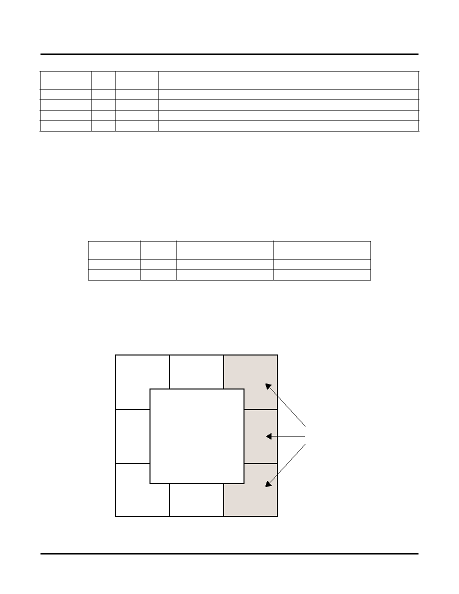
Floorplanning
The controller design uses two different I/O standards, HSTL1 for the QDR interface and LVTTL for the host inter-
face. The required voltages for the design are shown in the table below.
Because these two standards require different supply and input reference voltages, they can't be put into the same
I/O bank. This design can be fit into any ORCA Series 4 FPGA or FPSC devices. For demonstration purpose, the
ORSPI4 1036-ball fpSBGA package is chosen to be the target device. Figure 3 shows the available I/O banks and
the number of I/Os in the banks of an ORSPI4 FPSC 1036 fpSBGA package. All HSTL1 I/Os in the design are put
into I/O bank 7.
Figure 3. I/O Bank Assignments
qdrSA[19:0]
O
HSTL1
Address, connects to QDR "Address Inputs" SA
qdrD[15:0]
O
HSTL1
Write data, connects to QDR "Data Inputs" D
qdrPD[1:0]
O
HSTL1
Write parity, connects to QDR "Data Inputs" D
qdrBWN[1:0]
O
HSTL1
Byte write enable, active low, connects to QDR "Block Write Control Pin" /BW[1:0]
I/O Standard
V
DDIO
(V)
V
REF
(V)
Number of I/Os Required for
this Design
HSTL1
1.5
0.75
65
LVTTL
3.3
NA
121
Table 1. System Summary (Continued)
Signal Name
I/O
Type
I/O
Standard
Function/Connection Description
Used for
Embedded
Core I/Os
BANK 1
(TC)
116 I/Os
BANK 5
(BC)
106 I/Os
BANK 6
(BL)
112 I/Os
BANK 0
(TL)
96 I/Os
BANK 7
(CL)
98 I/Os
PLC
ARRAY

Lattice Semiconductor
QDR Memory Controller
4
Timing Waveforms
The QDR memory controller design has been verified through post-route timing simulation using the QDR memory
Verilog simulation model from a memory vender. The following figures are the timing waveforms of the memory
controller in read/write/nop operations running under 178MHz. For more detailed timing, please download the
design and run the timing simulation.
Figure 4. READ and NOP Timing Waveforms
Figure 5. WRITE and NOP Timing Waveforms
hostCLK
(178MHz)
hRA[ ]
hRN
hRQ[31:0]
qdrK
qdrKN
qdrSA[ ]
qdrRN
qdrQ[15:0]
Note: Q1-1 = Q1[31:16], Q1-2 = Q1[15:0], Q2-1 = Q2[31:16], Q2-2 = Q2[15:0].
READ
A1
READ
A2
NOP
READ
A3
NOP
NOP
NOP
NOP
NOP
NOP
NOP
A1
A1
A2
A3
A2
Q1-1 Q1-2 Q2-1 Q2-2
A3
Q3-1 Q3-2
Q1
Q2
NOP
hostCLK
(178MHz )
hWA[ ]
hWD[31:0]
hW N
h32
h16
qdrK
qdrKN
qdrSA[ ]
qdrW N
qdrD[15:0]
qdrBW[1]
qdrBW[0]
Notes:
1. According to h16 and h08 input values, the write cycles data width can be either 32-bit, 16-bit, or 8-bit.
Write cycle A1 is a 32-bit write access. Write cycles A2 and A3 are 16-bit write accesses. Write cycles A4,
A5, A6, A7 are 8-bit write accesses.
2. Dx-1 = Dx[31:16]. Dx-2 = Dx[15:0], where x = 1, 2, 3, 4, 5, 6, 7.
3. Bit-1 of address A2 is 0. Write cycle A2 will write only D2[31:16] to the memory.
4. Bit-1 of address A3 is 1. Write cycle A3 will write only D2[15:0] to the memory.
5. Bit-1 and bit-0 of address A4 are 0 and 0 respectively. Write cycle A4 will write only D4[31:24] to the memory.
5. Bit-1 and bit-0 of address A5 are 0 and 1 respectively. Write cycle A5 will write only D5[23:16] to the memory.
5. Bit-1 and bit-0 of address A6 are 1 and 0 respectively. Write cycle A6 will write only D6[15:8] to the memory.
5. Bit-1 and bit-0 of address A7 are 1 and 1 respectively. Write cycle A7 will write only D7[7:0] to the memory.
WRITE
A1
WRITE
A2
NOP
WRITE
A3
NOP
WRIT E
A4
WRITE
A5
WRIT E
A6
WRIT E
A7
NOP
NOP
NOP
A1
D1
A2
D2
A3
D3
A4
D4
A5
D5
A6
D6
A7
D7
hWA[1]=0
hWA[1]=1
hWA[1:0]=00 hWA[1:0]=01 hWA[1:0]=10 hWA[1:0]=11
A1
D1-1 D1-2
A2
D2-1 D2-2
A3
D3-1 D3-2
D4-1
A4
D4-2 D5-1
A5
D5-2 D6-1
A6
D6-2 D7-1
A7
D7-2

Lattice Semiconductor
QDR Memory Controller
5
Figure 6. READ, WRITE and NOP Timing Waveforms
Implementation
The design software used for this implementation is Lattice ispLEVER
Æ
. The following is the reference of imple-
mentation information of the design using Verilog language and Synplify synthesizer.
The source files and testbench are listed below:
1. Verilog Source:
∑ qdr2_io.v
Top-level file includes declarations of HSTL1 and LVTTL I/O standards.
∑ qdr2.v
Main module of the QDR Memory Controller.
∑ pipeline.v
Pipeline module for increasing performance.
2. Testbench:
∑ tb_qdr2.tf
Technical Support Assistance
Hotline: 1-800-LATTICE (North America)
+1-408-826-6002 (Outside North America)
e-mail:
techsupport@latticesemi.com
Internet: www.latticesemi.com
hostCLK
(178MHz )
hWA[ ]
hWD[31:0]
hW N
h16
h8
qdrK
qdrK N
qdrSA[ ]
qdrW N
qdrD[15:0]
qdrBW[1]
qdrBW[0]
WRIT E
A1
WRITE
A2
NOP
WRITE
A3
NOP
WRITE
A4
WRITE
A5
WRITE
A6
WRITE
A7
NOP
NOP
READ
A8
READ
A9
READ
A0
hRA[ ]
hRN
hRQ[31:0]
qdrR N
qdrQ[15:0]
Notes:
1. Dx-1 = Dx[31:16]. Dx-2 = Dx[15:0], where x = 1, 2, 3, 4, 5, 6, 7.
2. Qy-1 = Qy[31:16]. Qy-2 = Qy[15:0], where y = 8, 9, 0.
A1
D1-1 D1-2
A1
D1
A2
D2
A3
D3
A2
D2-1 D2-2
A4
D4
A5
D5
A6
D6
A3
D3-1 D3-2
D4-1
A4
D4-2
A7
D7
D5-1
A5
D5-2
hWA[1]=0
hWA[1]=1
D6-1
A6
D6-2 D7-1
A7
D7-2
hWA[1:0]=00 hWA[1:0]=01 hWA[1:0]=10 hWA[1:0]=11
A8
A9
A0
Q8
Q9
Q8-1 Q8-2 Q9-1 Q9-2
Q0-1 Q0-2
A8
A9
A0
NOP