 | –≠–ª–µ–∫—Ç—Ä–æ–Ω–Ω—ã–π –∫–æ–º–ø–æ–Ω–µ–Ω—Ç: SK70707 | –°–∫–∞—á–∞—Ç—å:  PDF PDF  ZIP ZIP |

SK70704/SK70707 or SK70708
1168 Kbps HSDL Data Pump Chip Set
Datasheet
The HDSL Data Pump is a chip set consisting of the following two devices:
s
SK70704 Analog Core Chip (ACC)
s
SK70707 (68-pin PLCC) or SK70708 (44-pin PLCC) HDSL Digital Transceiver (HDX)
The HDSL Data Pump is a 2-wire transceiver which provides echo-cancelling and 2B1Q line
coding. It incorporates transmit pulse shaping, filtering, line drivers, receive equalization, timing
and data recovery to provide 1168 kbps, clear-channel, "data pipe" transmission. The Data Pump
provides Near-End Cross-Talk (NEXT) performance in excess of that required over all ETSI test
loops. Typical transmission range on 0.4 mm cable exceeds 3.6 km in a noise-free environment
or 2.8 km with a 0 dB margin over 10
µ
V/
Hz ETSI noise.
The Data Pump meets the requirements of
ETSI ETR-152
. It provides one end of a single-channel
HDSL transmission system from the twisted pair interface back to the Data Pump/HDSL data
interface. The Data Pump can be used at either the NTU or the LTU end of the interface.
Applications
Product Features
s
E1 (2-pair) and fractional E1 transport
s
N-channel digital pair-gain
s
Wireless base station to switch interface
s
s
Campus and private networking
s
High-Speed digital modems
s
Fully integrated, 2-chip set for interfacing
to 2-wire HDSL lines at 1168 kbps
s
Single +5 V supply
s
Integrated line drivers, filters and hybrid
circuits result in greatly reduced external
logic and simplified support circuitry
requirements
s
Simple line interface circuitry, via
transformer coupling, to twisted pair line
s
Internal ACC voltage reference
s
Integrated VCO circuitry
s
Converts serial binary data to scrambled
2B1Q
encoded data
s
Self-contained activation/start-up state
machine for simplified single loop designs
s
Programmable for either line termination
(LTU) or network termination (NTU)
applications
s
Compliant with ETSI ETR-152 (1995)
s
Compliant with ITU G.991.1
s
Design allows for operation in either
Software Control or stand alone Hardware
Control mode
s
Typical power consumption less than 1.2 W
allowing remote power feeding for repeater
and NTU equipment
s
Input or Output Reference Clock of 18.688
MHz
s
Digital representation of receive signal
level and noise margin values available for
SNR controlled activation
As of January 15, 2001, this document replaces the Level One document
Order Number:
249193-001
SK70704/SK70707 or SK70708 -- 1168 Kbps HSDL Data Pump Chip Set.
January 2001

Datasheet
Information in this document is provided in connection with Intel
Æ
products. No license, express or implied, by estoppel or otherwise, to any intellectual
property rights is granted by this document. Except as provided in Intel's Terms and Conditions of Sale for such products, Intel assumes no liability
whatsoever, and Intel disclaims any express or implied warranty, relating to sale and/or use of Intel products including liability or warranties relating to
fitness for a particular purpose, merchantability, or infringement of any patent, copyright or other intellectual property right. Intel products are not
intended for use in medical, life saving, or life sustaining applications.
Intel may make changes to specifications and product descriptions at any time, without notice.
Designers must not rely on the absence or characteristics of any features or instructions marked "reserved" or "undefined." Intel reserves these for
future definition and shall have no responsibility whatsoever for conflicts or incompatibilities arising from future changes to them.
The SK70704/SK70707 or SK70708 may contain design defects or errors known as errata which may cause the product to deviate from published
specifications. Current characterized errata are available on request.
Contact your local Intel sales office or your distributor to obtain the latest specifications and before placing your product order.
Copies of documents which have an ordering number and are referenced in this document, or other Intel literature may be obtained by calling 1-800-
548-4725 or by visiting Intel's website at http://www.intel.com.
Copyright © Intel Corporation, 2001
*Third-party brands and names are the property of their respective owners.

Datasheet
3
1168 Kbps HSDL Data Pump Chip Set -- SK70704/SK70707 or SK70708
Contents
1.0
Pin Assignments and Signal Description
........................................................ 8
2.0
Functional Description
........................................................................................... 15
2.1
Transmit .............................................................................................................. 15
2.2
Receive ............................................................................................................... 15
2.3
Control................................................................................................................. 15
2.4
ACC and HDX Overview ..................................................................................... 15
2.4.1
Analog Core Chip (ACC) ........................................................................ 15
2.4.2
HDSL Digital Transceiver (HDX) ............................................................ 16
2.4.3
HDX/ACC Interface ................................................................................ 17
2.5
Line Interface....................................................................................................... 17
2.6
HDSL Data Interface ........................................................................................... 18
2.7
Microprocessor Interface (HDX).......................................................................... 21
2.7.1
Control Pins............................................................................................ 21
2.7.2
Register Access ..................................................................................... 22
2.7.3
Registers ................................................................................................ 23
2.8
Activation State Machines ................................................................................... 29
2.8.1
LTU Data Pump Activation .....................................................................29
2.8.2
LTU Framer Activation ........................................................................... 31
2.8.3
NTU Data Pump Activation .................................................................... 33
2.8.4
NTU Framer Activation ........................................................................... 33
2.8.5
HDSL Synchronization State Machine ................................................... 33
3.0
Application Information
.........................................................................................37
3.1
HDSL Framer State Machine Design .................................................................. 37
3.2
PCB Layout ......................................................................................................... 37
3.2.1
User Interface .........................................................................................37
3.2.2
Digital Section ........................................................................................ 38
3.2.3
Analog Section ....................................................................................... 38
4.0
Test Specifications
.................................................................................................. 44
5.0
Mechanical Specifications
.................................................................................... 53

SK70704/SK70707 or SK70708 -- 1168 Kbps HSDL Data Pump Chip Set
4
Datasheet
Figures
1
SK70704/SK70707 or SK70708 Block Diagram ................................................... 7
2
Package Markings................................................................................................. 7
3
SK70704 ACC Pin Locations ................................................................................ 8
4
SK70707/SK70708 HDX Pin Assignments ........................................................... 9
5
HDX/ACC Interface ≠ Relative Timing ................................................................ 18
6
HDX/ACC Framer Interface ≠ Relative Timing.................................................... 20
7
Model for HDSL Data Pump and HDSL Framer Applications ............................. 21
8
LTU Data Pump Activation State Machine .......................................................... 32
9
LTU HDSL Framer Activation State Machine...................................................... 32
10
NTU Data Pump Activation State Machine ......................................................... 34
11
NTU HDSL Framer Activation State Machine ..................................................... 35
12
HDSL Synchronization State Machine ................................................................ 36
13
PCB Layout Guidelines ....................................................................................... 39
14
Typical Support Circuitry for LTU Applications.................................................... 40
15
Typical Support Circuitry for NTU Applications ................................................... 42
16
SK70707/SK70708 HDX Control and Status Signals (Hardware Mode) ............ 43
17
ACC Normalized Pulse Amplitude Transmit Template ....................................... 45
18
ACC Transmitter Timing...................................................................................... 46
19
Upper Bound of Transmit Power Spectral Density.............................................. 46
20
ACC Receiver Syntax and Timing....................................................................... 47
21
HDX/HDSL Data Interface Timing....................................................................... 49
22
Reset and Interrupt Timing (mP Control Mode) ................................................. 51
23
Parallel Data Channel Timing ............................................................................ 52
24
ACC Plastic Leaded Chip Carrier Package Specifications ................................ 53
25
HDX Plastic Leaded Chip Carrier Package Specifications ................................. 54
Tables
1
SK70704 ACC Pin Assignments/Signal Descriptions ........................................... 9
2
SK70707/SK70708 HDX Pin Assignments/Signal Descriptions ......................... 11
3
ACC Transmit Control ......................................................................................... 17
4
HDX/ACC Serial Port Word Bit Definitions (
Figure 5
) ........................................ 18
5
HDSL Framer TDATA Requirements .................................................................. 19
6
Register Summary .............................................................................................. 23
7
Main Control Register WR0 ................................................................................ 23
8
Interrupt Mask Register WR2 .............................................................................. 24
9
Read Coefficient Select Register WR3 ............................................................... 25
10
Main Status Register RD0................................................................................... 25
11
Receiver Gain Word Register ............................................................................. 26
12
Noise Margin Register RD2
Noise Margin Coding126
13
Coefficient Read Register ................................................................................... 28
14
Activation Status Register RD5........................................................................... 28
15
Receiver AGC and FFE Step Gain Register RD6 ............................................... 29
16
Data Pump/Framer Activation State Machine Correspondences........................ 30
17
Activation ≠ Synchronization ............................................................................... 33
18
Components for Suggested Circuitry (
Figure 14
and
Figure 15
) ........................ 40
19
Transformer Specifications
(
Figure 14
and
Figure 15
, Reference T1)41

Datasheet
5
1168 Kbps HSDL Data Pump Chip Set -- SK70704/SK70707 or SK70708
20
Crystal Specifications
(
Figure 14
and
Figure 15
, Reference Y1)41
21
ACC Absolute Maximum Ratings ........................................................................ 44
22
ACC Recommended Operating Conditions......................................................... 44
23
ACC DC Electrical Characteristics (Over Recommended Range) ...................... 44
24
ACC Transmitter Electrical Parameters (Over Recommended Range) .............. 45
25
ACC Receiver Electrical Parameters (Over Recommended Range) ..................46
26
HDX Absolute Maximum Ratings ........................................................................ 47
27
HDX Recommended Operating Conditions......................................................... 47
28
HDX DC Electrical Characteristics (Over Recommended Range) ...................... 48
29
HDX/HDSL Data Interface Timing (
Figure 21
) .................................................... 48
30
HDX/Microprocessor Interface Timing Specifications1 (
Figure 22
and
Figure 23
) .
50
31
General System and Hardware Mode Timing ..................................................... 50
SK70704/SK70707 or SK70708 -- 1168 Kbps HSDL Data Pump Chip Set
6
Datasheet
Revision History
Revision
Date
Description
1168 Kbps HSDL Data Pump Chip Set -- SK70704/SK70707 or SK70708
Datasheet
7
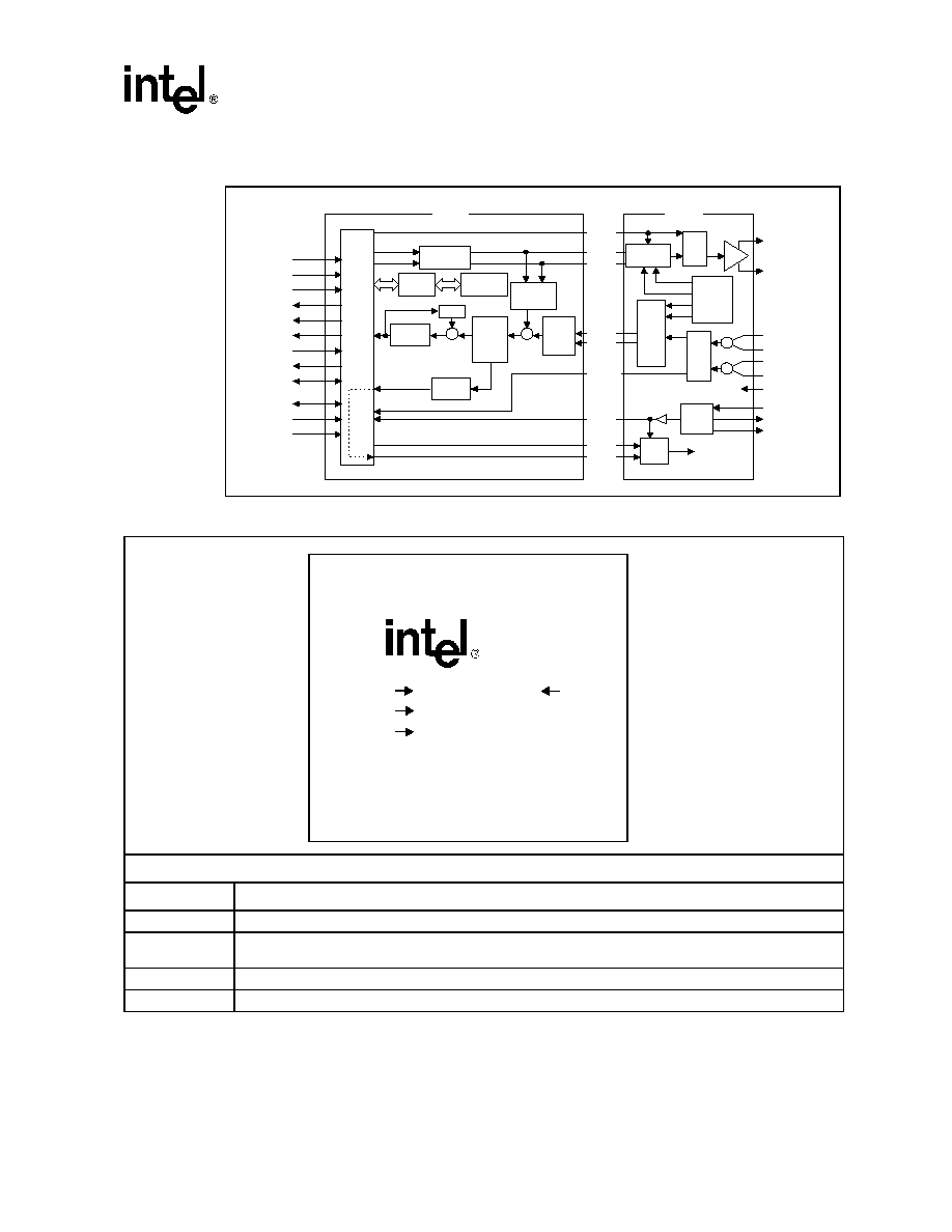
Figure 1. SK70704/SK70707 or SK70708 Block Diagram
Figure 2. Package Markings
Package Topside Markings
Marking
Definition
Part #
Unique identifier for this product family.
Rev #
Identifies the particular silicon "stepping" -- refer to the specification update for additional stepping
information.
Lot #
Identifies the batch.
FPO #
Identifies the Finish Process Order.
o
Back
End
Control
Logic
Deci-
mation
Filter
DFE
Phase
Detector
CK9M
TDATA
TFP
RDATA
RFP
ICLK
LTU
LOSW
REFCLK
DATA
ADDR
CTRL
ACC
Line
Driver
A/
D
M
odulator
AGC
To Various
Blocks
VPLL
TCK4M
TSGN
TMAG
AD0
AD1
AGCKIK
CK37M
FS
DTR
HDX
XO
XI
IBIAS
BTIP
RRING
BRING
RTIP
TTIP
TRING
VREF
Tx
Filter
Activation
Control
Decision
Circuit
FFE
DAGC
AGC
Tap
Echo
Canceller
2B1Q
Encoder
Serial
I/F
Scrambler
VCO
XXXXXXXX XX
XXXXXX
XXXXXXXX
Part #
LOT #
FPO #
Rev #
SK70704/SK70707 or SK70708 -- 1168 Kbps HSDL Data Pump Chip Set
8
Datasheet
1.0
Pin Assignments and Signal Description
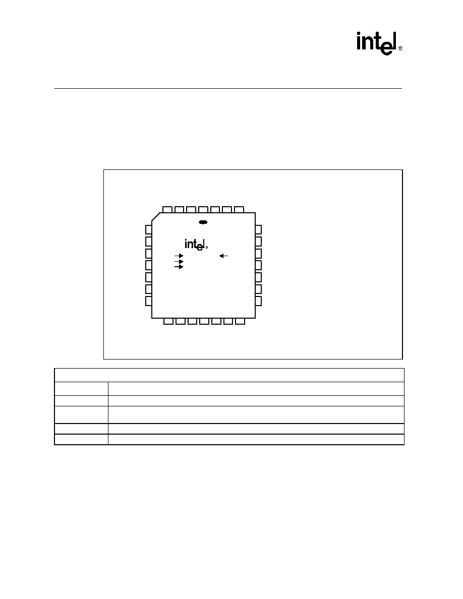
The ACC is packaged in a 28-pin PLCC.
Figure 3
shows the ACC pin locations.
Table 1
lists signal
descriptions for each pin, except pins 18 and 19 which are not connected.
The HDX is available in two packages: 68-pin PLCC (SK70707) and 44-pin PLCC (SK70708).
Figure 4
shows the HDX pin assignments.
Table 2
lists signal descriptions for each pin,
corresponding to the specific package.
Figure 3. SK70704 ACC Pin Locations
Package Topside Markings
Marking
Definition
Part #
Unique identifier for this product family.
Rev #
Identifies the particular silicon "stepping" -- refer to the specification update for additional stepping
information.
Lot #
Identifies the batch.
FPO #
Identifies the Finish Process Order.
1
2
3
4
5
6
7
8
9
10
11
12 13 14 15 16 17 18
19
20
21
22
23
24
25
26
27
28
DT
R
FS
AD0
AD1
AG
CKIK
TC
K4M
TM
AG
TSGN
DVCC
TVCC
TRING
TTIP
TGND
n/c
RVC
C
RT
I
P
RG
ND
RR
IN
G
BTIP
BR
IN
G
n/
c
CK37M
DGND
XO
XI
VPLL
PGND
IBIAS
SK70704PE XX
XXXXXX
XXXXXXXX
Part #
LOT #
FPO #
Rev #

1168 Kbps HSDL Data Pump Chip Set -- SK70704/SK70707 or SK70708
Datasheet
9
Figure 4. SK70707/SK70708 HDX Pin Assignments
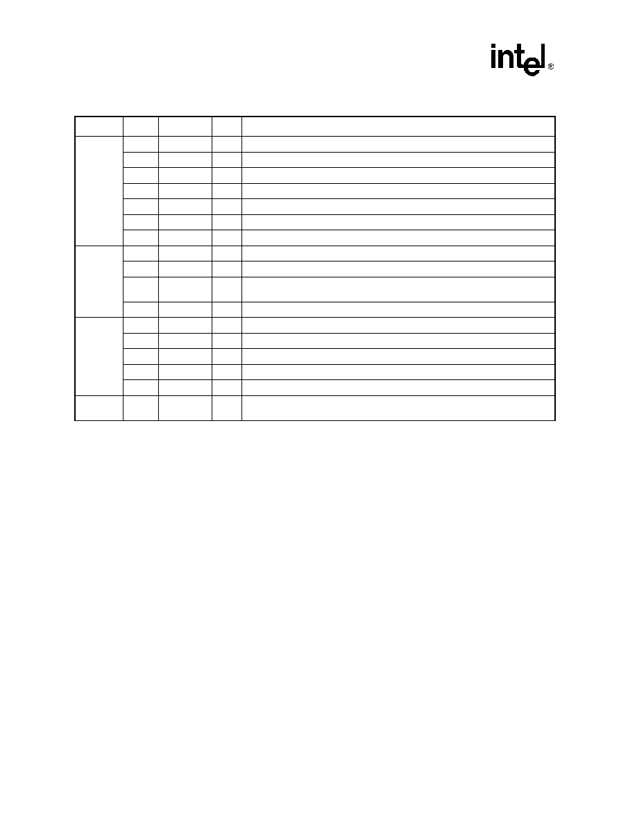
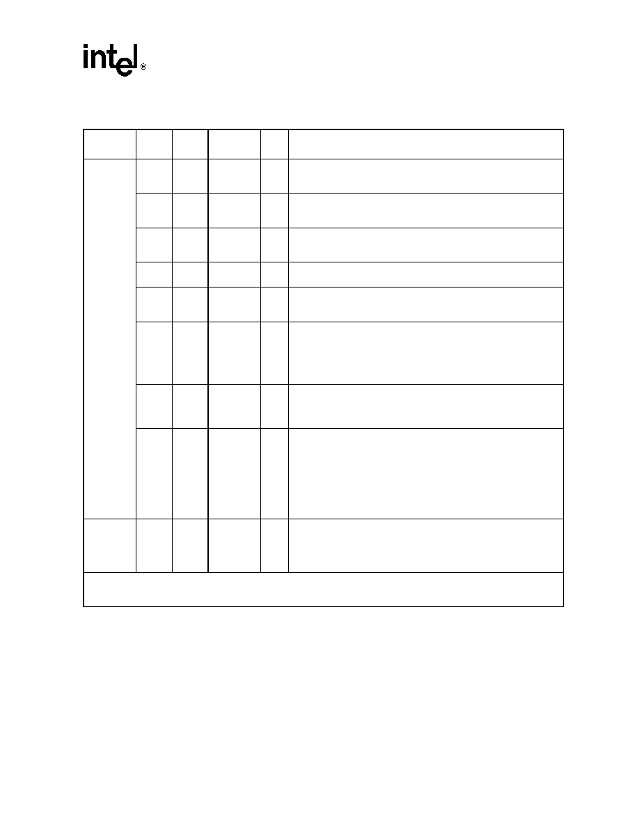
Table 1. SK70704 ACC Pin Assignments/Signal Descriptions
Group
Pin #
Symbol
I/O
Description
Line
13
RTIP
I
Receive Tip and Ring. Connected these input pins to the line transformer per
network requirements.
14
RRING
I
16
BTIP
I
Bias Tip and Ring. Inputs provide a bias setting for the receiver. Provide balanced
network inputs.
17
BRING
I
21
TTIP
O
Transmit Tip and Ring. Line driver outputs.
22
TRING
O
PLL
7
XO
O
Crystal Oscillator. Connect a 37.376 MHz crystal across these two pins.
8
XI
I
9
VPLL
O
PLL Voltage Control. Supplies control voltage to the VCO.
NOTE: Pin Functions in Hardware Control Mode are shown in parentheses.
1
2
3
4
5
6
7
8
9
10
11
12
13
14
15
16
17
18
19
20
21
22
23
24
25
26
27 28 29 30 31 32 33 34 35 36 37 38 39 40 41 42 43
44
45
46
47
48
49
50
51
52
53
54
55
56
57
58
59
60
61
62
63
64
65
66
67
68
VCC1
GND
1
GND
2
ADDR
0 (
Q
UI
ET)
ADDR
1 (
ACTR
E
Q)
ADDR
2
ADDR
3 (
ACTV
N
G)
RDAT
A
RFP
n/c
n/c
n/c
n/c
RFST
DATA
TFP
FCLK
CK9M
MEN
LTU
ICLK
n/c
n/c
n/c
n/c
n/
c
n/
c
n/
c
n/
c
n/
c
CK3
7M
DTR
FS
AD
0
AD
1
AGC
K
IK
T
CK4M
TM
A
G
TS
G
N
n/
c
GND
3
n/
c
n/c
n/c
n/c
GND4
n/c
LOSW
D0 (LOST,LOS)
n/c
n/c
n/c
n/c
n/c
D7 (T
XTST)
D6 (R
CLKU
)
D5 (B
ELB)
D4 (F
ELB)
D1 (LO
S
WT)
D2 (ILMT
)
D3 (RPT
R)
VCC2
SET2
RESET1
INT (TEXP)
CHIPSEL
WRITE
READ
6
5
4
3
2
1 44 43 42 41 40
39
38
37
36
35
34
33
32
31
30
29
18 19 20
21 22 23 24 25 26 27 28
FS
DTR
CK
37M
R
ESE
T
2
AG
C
K
I
K
AD
1
AD
0
17
16
15
14
13
12
11
10
9
8
7
ICLK
LTU
CK9MEN
CK9M
REFCLK
TFP
TDATA
RFST
ADDR3(ACTVNG)
RDATA
RFP
n/c
LOSW
RESET1
INT(TEXP)
CHIPSEL
WRITE
READ
D0(LOST, LOS
D1(LOSWT)
D2(ILMT)
D3(RPTR)
TCK
4
M
G
ND3
TS
GN
TM
A
G
G
ND2
A
DDR0(
Q
UIE
T
)
A
DDR1(
A
CTRE
Q
)
A
DDR2
V
CC2
V
CC1
G
ND1
D
7
(
T
XT
ST
)
D4
(
F
E
L
B
)
D
5
(
B
ELB)
D6
(
RCL
K
U
)
SK70707PE XX
XXXXXX
XXXXXXXX
Part #
LOT #
FPO #
Rev #
SK70708PE XX
XXXXXX
XXXXXXXX
Part #
LOT #
FPO #
Rev #
SK70704/SK70707 or SK70708 -- 1168 Kbps HSDL Data Pump Chip Set
10
Datasheet
Power
10
PGND
I
PLL Ground. 0 V.
12
RVCC
I
Power supply. + 5 V (± 5%).
23
TVCC
I
Power supply. + 5V (± 5%).
24
DVCC
I
Digital Power Supply. +5 V (± 5%).
6
DGND
I
DVCC Ground. 0V.
15
RGND
I
RVCC Ground. 0V.
20
TGND
I
TVCC Ground. 0V.
Clock and
Control
3
FS
I
584 kHz clock. Input from HDX FS.
4
DTR
I
Serial control data. Input from the HDX at 18.688 Mbps.
5
CK37M
O
37.376 MHz HDSL Reference Clock. Used as the receive timing reference for the
HDX. Tie to HDX CK37M.
27
TCK4M
I
4.672 MHz Clock. Input from HDX TCK4M.
Data Input
and
Output
28
AGCKIK
O
AGC adjust signal. Output to HDX AGCKIK.
1
AD1
O
A-to-D converter data line 1. Connect to HDX AD1.
2
AD0
O
A-to-D converter data line 0. Connect to HDX AD0.
25
TSGN
I
Transmit quat sign. Input from HDX.
26
TMAG
I
Transmit quat magnitude. Input from HDX.
Analog
Input
11
IBIAS
I
Input BIAS. Provides input bias current.
Table 1. SK70704 ACC Pin Assignments/Signal Descriptions (Continued)
Group
Pin #
Symbol
I/O
Description
1168 Kbps HSDL Data Pump Chip Set -- SK70704/SK70707 or SK70708
Datasheet
11
Table 2. SK70707/SK70708 HDX Pin Assignments/Signal Descriptions
Group
707
Pin #
708
Pin #
Symbol
I/O
Description
User Port
14
10
RFST
O
Receive Frame and Stuff Bit Indicator. Goes High for 18 consecutive
ICLK periods to indicate four stuffing bits
(b7007 - 7010) and 14 frame bits (b1-14) on RDATA.
17
13
REFCLK
I
1
O
18.688 MHz HDSL Reference Clock. In LTU Mode, this clock generates
transmit and receive timing and must have ±32 ppm accuracy. In NTU
Mode, this output is derived by dividing CK37M by two.
20
16
LTU
I
Operation Mode Select. When LTU is High, the Data Pump operates in
LTU mode; when LTU is Low, the Data Pump operates in NTU mode.
Tied to internal pull-up device.
21
17
ICLK
O
Bit Rate Clock. Nominally 1168 kHz, REFCLK is the source of ICLK in
LTU Mode. CK37M is the source of ICLK in NTU Mode.
49
30
LOSW
O
Loss of Sync Word Indicator. Normally Low in Active States, goes
High to indicate receipt of six consecutive mismatched frame synch
words. LOSW is logic High in all states except Active States.
8
8
RDATA
O
Receive HDSL Data Stream. Output data to HDSL framer at 1168 kbps:
HDSL payload of Loop 1 or Loop 2 bytes plus the Z-bits,
eoc, crc, losd, febe, ps, bpv, hrp, indc/indr and uib bits,
Sync bits for frame positions b1-14,
Stuff bits for frame positions b7007 - 7010.
RDATA bits are forced high in all states except the Active State.
9
7
RFP
O
Receive Frame Pulse. Low for one ICLK cycle during the last bit of the
current HDSL receive frame on RDATA, either b7006 or b7010. Period
is within one baud time of 6 ms.
2
RFP is valid when LOSW transitions
Low.
15
11
TDATA
I
1
Transmit HDSL Data Stream. Input data from HDSL framer at
1168 kbps:
HDSL payload of Loop 1 or Loop 2 bytes plus the Z-bits,
eoc, crc, losd, febe, ps, bpv, hrp, indc/indr and uib bits,
Sync bits for frame positions b1-14,
Stuff dummy bits; may be 1s or 0s.
Tied to internal pull-up device.
When ACTIVE, the Data Pump is transparent and the HDSL framer must
generate the appropriate bits on TDATA as shown in
Table 5
.
User Port
16
12
TFP
I
1
Transmit Frame Pulse. Must be Low for one ICLK cycle during the last
bit of the current HDSL frame on TDATA, either b7006 or b7010. Period
is within one baud time of 6 ms.
2
If TFP is pulled Low and is Low again
three ICLK cycles later, RDATA, RFP, RFST, ICLK, CK9MEN and LOSW
go to tri-state. Tied to internal pull-up device.
1. This input is a Schmidt Triggered circuit and includes an internal pull-up device.
2. The period is 6 ms ±
1
/
584
ms.
3. This input is a Schmidt Triggered circuit and includes an internal pull-down device.
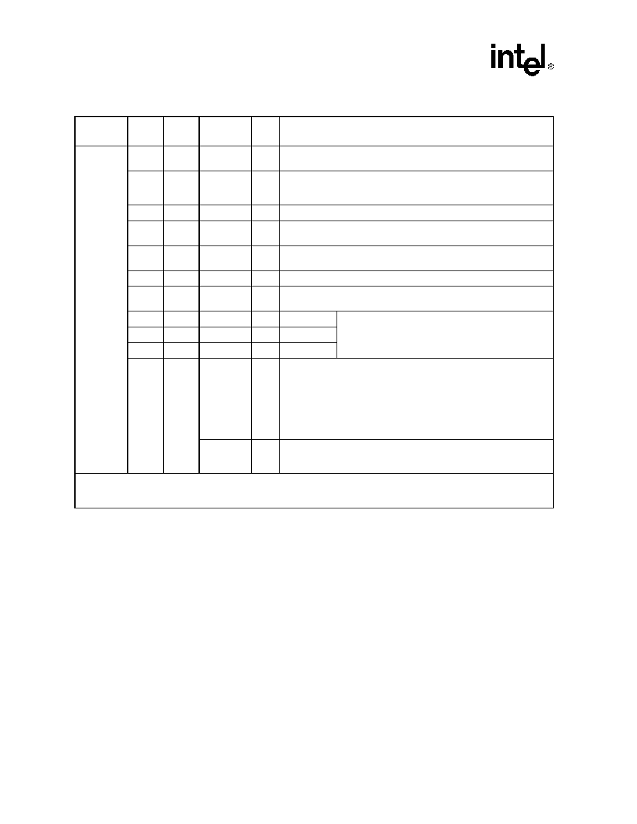
SK70704/SK70707 or SK70708 -- 1168 Kbps HSDL Data Pump Chip Set
12
Datasheet
Hardware
Interface
(Hardware
Control
Mode)
4
4
QUIET
I
3
Quiet Mode Enable. Pull High to force HDX into Deactivated State. Any
later transition to Low will not return HDX to Active State. See ACTREQ.
5
5
ACTREQ
I
3
Activation Request (LTU mode) or no function (NTU mode). Tie this
pin Low in NTU mode. If QUIET is Low, a rising edge on this pin initiates
activation, but the signal is ignored after activation. See QUIET.
6
6
reserved
≠
Pull Low in LTU mode, leave open in NTU mode.
7
9
ACTVNG
O
Activating State Indication. High when the HDX is in the Activating
State.
23
18
RESET2
I
1
Reset Pulse. Pull Low on power up to initialize circuits and stop all
clocks.
50
31
RESET1
I
1
Reset Pulse. Pull Low to initialize internal circuits.
51
32
TEXP
O
Timer Expiry. Goes High to indicate 30 second timer expiration in all
states.
52
33
CHIPSEL
I
3
Chip Select
Assert these three pins Low to activate Hardware
Control Mode. When any of them goes High, the HDX
reverts immediately to Software Control Mode.
53
34
WRITE
I
3
Write Pulse
54
35
READ
I
3
Read Pulse
55
36
LOST
(LTU)
O
Loss of Signal Timer Expiration. In LTU mode, LOST goes High when
the Data Pump enters the Inactive State. The transition from the
Deactivated to the Inactive State occurs 1 second after the end of
transmission by the NTU when deactivation began from either the
Active-1 or Active-2 State. When the Data Pump transitions from the
Activating State to the Deactivated State it may immediately enter the
Inactive State without waiting for NTU transmission to cease. (See
Figure 7
.)
LOS
(NTU)
O
Loss of Signal Energy Indicator. In NTU mode LOS goes High to
indicate loss of signal energy on entering the Inactive State (See
Figure
10
).
Table 2. SK70707/SK70708 HDX Pin Assignments/Signal Descriptions (Continued)
Group
707
Pin #
708
Pin #
Symbol
I/O
Description
1. This input is a Schmidt Triggered circuit and includes an internal pull-up device.
2. The period is 6 ms ±
1
/
584
ms.
3. This input is a Schmidt Triggered circuit and includes an internal pull-down device.
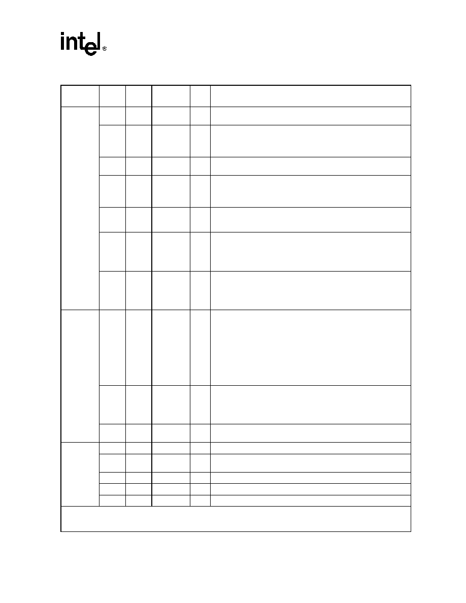
1168 Kbps HSDL Data Pump Chip Set -- SK70704/SK70707 or SK70708
Datasheet
13
Hardware
Interface
(Hardware
Control
Mode)
-cont'd
63
37
LOSWT
O
Loss of Sync Word Timer. LOSWT goes High when LOSW is
sustained for longer than 2 sec.
62
38
ILMT
I
1
Insertion Loss Measurement Test. Set High to transmit a framed &
scrambled, "all 1s", 2B1Q pulse sequence. Pulse sequence will have a
valid sync word. In the NTU configuration, when the ILMT mode is
selected, the Data Pump may begin activation.
61
39
RPTR
I
1
Repeater Mode Enable. When in LTU mode, ICLK output phase is
aligned to the TFP input pulse width. Ignored in NTU mode.
64
40
FELB
I
1
Front-End Loopback (LTU only). In Inactive State, set High to cause
the ACC to loopback. The returned signal activates the HDX which
receives its own transmitted data. The system ignores incoming data
from NTU during loopback irrespective of status.
65
41
BELB
I
1
Back-End Loopback. In Active State a High forces an internal,
transparent loopback with RDATA connected to TDATA and RFP
connected to TFP.
66
42
RCLKU
O
Receive Baud Rate (584 kHz) Clock. Aligned with ICLK in NTU mode,
phase synchronous with receive pulse stream, However, during
Activating State, the clocks may not be aligned. In the LTU mode
RCLKU has a constant, arbitrary, phase relationship with ICLK in Active
State.
67
43
TXTST
I
1
Transmit Test. Set high to enable isolated transmit pulse generation.
The time between pulses is approximately 6 ms. TDATA controls the
sign and TFP controls the magnitude of the transmitted quat pulses
according to the 2B1Q encoding rules. In the NTU configuration, when
the TXTST mode is selected, the Data Pump may begin activation.
Processor
Interface
(Software
Control
Mode)
55
63
62
61
64
65
66
67
36
37
38
39
40
41
42
43
D0
D1
D2
D3
D4
D5
D6
D7
I
1
/O
I
1
/O
I
1
/O
I
1
/O
I
1
/O
I
1
/O
I
1
/O
I
1
/O
Data bit 0. Eight-bit, parallel data bus.
Data bit 1
Data bit 2
Data bit 3
Data bit 4
Data bit 5
Data bit 6
Data bit 7
4
5
6
7
4
5
6
9
ADDR0
ADDR1
ADDR2
ADDR3
I
3
I
3
I
3
I
3
Address bit 0. Four-bit address, selects read or write register.
Address bit 1
Address bit 2
Address bit 3
23
18
RESET2
I
1
Reset Pulse. Pull Low on power up to initialize circuits and stop all
clocks.
Processor
Interface
(Software
Control
Mode)
50
31
RESET1
I
1
Reset Pulse. Pull Low to initialize internal circuits. ICLK continues.
51
32
INT
O
Interrupt Output. Open drain output. Requires an external 10 k
pull
up resistor. Goes Low on interrupt.
52
33
CHIPSEL
I
3
Chip Select. Pull Low to read or write to registers.
53
34
WRITE
I
3
Write Pulse. Pull Low to write to registers.
54
35
READ
I
3
Read Pulse. Pull Low to read from registers.
Table 2. SK70707/SK70708 HDX Pin Assignments/Signal Descriptions (Continued)
Group
707
Pin #
708
Pin #
Symbol
I/O
Description
1. This input is a Schmidt Triggered circuit and includes an internal pull-up device.
2. The period is 6 ms ±
1
/
584
ms.
3. This input is a Schmidt Triggered circuit and includes an internal pull-down device.

SK70704/SK70707 or SK70708 -- 1168 Kbps HSDL Data Pump Chip Set
14
Datasheet
Clock and
Control
18
14
CK9M
I
3
9.344 or 18.688 MHz Reference Clock. Mandatory in NTU mode. Tie
High or Low in LTU Mode. Clock input requires ± 32 ppm accuracy.
19
15
CK9MEN
O
CK9M Enable. Active High enable for CK9M clock. In NTU mode, this
pin goes Low to indicate the PLL is tracking the input signal from the
LTU. Not used in LTU.
32
19
CK37M
I
Receive Timing Clock (37.376 MHz). Tie to CK37M on ACC.
33
20
DTR
O
Serial Control Data Link. Transfers data at 18.688 Mbps. Tie to DTR
on ACC.
34
21
FS
O
584 kHz Clock. Derived from CK37M. Tie to FS on ACC.
35
22
AD0
I
Analog to Digital Converter input pin. Tie to AD0 on ACC.
36
23
AD1
I
Analog to Digital Converter input pin. Tie to AD1 on ACC.
37
24
AGCKIK
I
AGC Adjust. Controls analog gain circuit. Tie to AGCKIK on ACC.
38
25
TCK4M
O
Transmit Clock. Tie to TCK4M on ACC.
39
26
TMAG
O
Transmit Magnitude Bit. Tie to TMAG on ACC.
40
27
TSGN
O
Transmit Sign Bit. Tie to TSGN on ACC.
Power
1
1
VCC1
I
Logic supply input (Refer to Table
Table 27
).
68
44
VCC2
I
I/O supply input.
2
2
GND1
I
Ground.
3
3
GND2
I
Ground.
42
28
GND3
I
Ground.
47
≠
GND4
I
Ground.
Misc
10 11
12 13
22 24
25 26
27 28
29 30
31 41
43 44
45 46
48 56
57 58
59 60
29
≠
≠
No internal connection.
Table 2. SK70707/SK70708 HDX Pin Assignments/Signal Descriptions (Continued)
Group
707
Pin #
708
Pin #
Symbol
I/O
Description
1. This input is a Schmidt Triggered circuit and includes an internal pull-up device.
2. The period is 6 ms ±
1
/
584
ms.
3. This input is a Schmidt Triggered circuit and includes an internal pull-down device.

1168 Kbps HSDL Data Pump Chip Set -- SK70704/SK70707 or SK70708
Datasheet
15
2.0
Functional Description
The HDSL Data Pump is a fully-integrated, two-chip solution (see front page block diagram)
which includes an SK70704 Analog Core Chip (ACC) and an SK70707/SK70708 HDSL Digital
Transceiver (HDX).
2.1
Transmit
The transmit data stream is supplied to the HDX at the TDATA input in a binary fashion. The HDX
scrambles and 2B1Q encodes the data and adds the sync word and stuff quats based on the TFP
frame pulse position. The injected stuff quats in a frame are equal to the last scrambled data symbol
in that frame. The 2B1Q encoded transmit quat data stream (TSGN/TMAG) is then passed to the
ACC which filters and drives it onto the line.
2.2
Receive
The composite waveform of the receive signal plus trans-hybrid echo is filtered and converted to
digital words at a rate of 584 k-words/second in the ACC. The ACC passes the digitized receive
quat stream (AD0 and AD1) to the HDX. The HDX performs digital filtering, linear echo
cancellation, frame recovery and descrambling. The HDX uses the transmit quat stream to generate
the echo estimates and estimate error values. Using this error and the delayed transmit quat stream,
the echo canceller coefficients are updated. The recovered, decoded and descrambled data is then
output to the framer-mux from the HDX RDATA pin.
2.3
Control
The Data Pump offers two control modes - Hardware Mode and Software Mode. In Hardware
mode the HDX receives control inputs via individually designated pins. In Software mode the
HDX control data is supplied via an 8-bit parallel port. In either mode, the HDX and the ACC
communicate via a unidirectional serial port (DTR).
2.4
ACC and HDX Overview
The following paragraphs describe the chip set components individually with reference to internal
functions and the interfaces between Data Pump components.
2.4.1
Analog Core Chip (ACC)
The ACC incorporates the following analog functions:
∑
the transmit line driver
∑
transmit and receive filters
∑
Phase-Locked Loop (PLL), including VCO
∑
hybrid circuitry analog-to-digital converter

SK70704/SK70707 or SK70708 -- 1168 Kbps HSDL Data Pump Chip Set
16
Datasheet
The ACC provides the complete analog front end for the HDSL Data Pump. It performs transmit
pulse shaping, line driving, receive A/D, and the VCO portion of the receiver PLL function.
Transmit and receive controls are implemented through the serial port. The ACC line interface uses
a single twisted pair line for both transmit and receive.
Table 2
lists the ACC pin descriptions.
Refer to Test Specifications section for ACC electrical and timing specifications.
2.4.1.1
ACC Transmitter
The ACC performs the pulse shaping and driving functions. The ACC transmitter generates a 4-
level output of 1/(8*f(TCK4M)) defined by TMAG and TSGN.
Table 3
lists 2B1Q pulse coding
parameters. Refer to Test Specifications for frequency and voltage templates.
2.4.1.2
ACC Receiver
The ACC receiver is a sophisticated sigma-delta converter. It sums the differential signal at RTIP/
RRING minus the signal at BTIP/BRING. The first A/D signal comes out of AD0 at a bit stream
rate of 18.688 MHz. The second stage of the A/D samples the noise of the first and generates the
AD1 bit stream at 18.688 MHz.
Receiver gain is controlled by the HDX via the AGC2-0 bits in the DTR serial control stream. The
AGCKIK output from the ACC is normally Low. It goes High when the signal level in the sigma-
delta A/D is approaching its clipping level, signaling the HDX to lower the gain.
The VCO is part of a phase-locked loop (PLL) locked to the receive data baud rate using an
external phase detector. The VCO frequency is varied by pulling an external crystal with external
varactor diodes that are controlled by the VPLL output. The VPLL output is, in turn, controlled by
the serial port VCO and PLL bits.
2.4.2
HDSL Digital Transceiver (HDX)
The HDX incorporates the following digital functions:
∑
bit-rate transmit and receive signal-processing
∑
adaptive echo-cancelling (EC)
∑
adaptive decision feedback-equalization (DFE) using the receive quat stream and the internal
error signal
∑
fixed and adaptive digital-filtering functions
∑
activation/start-up control and the microprocessor interface to the HDSL framer
The HDX also provides the Data Pump Back-End interface for the customer defined/developed
HDSL framer via serial data channels and clock signals. A simple, parallel 8-bit microprocessor
interface on the HDX allows high-speed access to control, status and filter coefficient words.
Table 2
lists the HDX pin descriptions. Refer to Test Specifications section for HDX electrical and
timing specifications.
The microprocessor interface on the HDX provides bit flags for signal presence, synchronization,
activation completion, and loss of synchronization for a time greater than two seconds. Single-byte
words representing receive signal level and the noise margin of the transceiver are also available on
the microprocessor interface. One control byte allows the user to start the Data Pump activation
sequence. The HDX controls the complete activation/start-up sequence, allowing flexible, single-
loop, fractional applications.

1168 Kbps HSDL Data Pump Chip Set -- SK70704/SK70707 or SK70708
Datasheet
17
2.4.3
HDX/ACC Interface
The ACC provides the 37.376 MHz master clock, CK37M, to the HDX. The serial control stream
framing signal FS is sampled inside the ACC with the CK37M rising edge. The serial control
stream, DTR, is sampled inside the ACC by the rising edge of an internally-generated clock at
f(CK37M)/2. This ACC internal clock has the same phase relationship with a similar clock inside
the HDX, as established by the FS signal. In the HDX, the half-rate clock CK37M/2 and FS
transition on the rising edge of CK37M, and DTR transitions come on the falling edge of CK37M/
2. The output REFCLK in NTU Mode equals CK37M/2.
The A/D converter outputs, AD0 and AD1, are clocked out of the ACC with CK37M, having
transitions coincidental with the rising edge of CK37M/2. The HDX samples AD0 and AD1 with
the falling edge of its internal CK37M/2.
Transmit data, represented by TSGN and TMAG, is clocked from the HDX using the falling edge
of TCK4M, the 4.672 MHz (f(REFCLK)/4) transmit time base clock. The ACC uses the rising
edge of TCK4M to sample TSGN and TMAG. TSGN and TMAG change state at the baud rate, or
every 8 cycles of TCK4M.
Figure 5
shows relative timing for the HDX/ACC interface.
2.4.3.1
HDX/ACC Serial Port
The HDX continually writes to the ACC serial port. This serial stream consists of two 16-bit words
as shown in Table
Table 4
. The data flows from the HDX to the ACC at a rate of f(CK37M)/2.
Refer to the Test Specifications section for serial port timing relationships and electrical
parameters.
2.5
Line Interface
The Data Pump line interface consists of three differential pairs. The transmit outputs TTIP and
TRING, receive inputs RTIP and RRING, and the balance inputs BTIP and BRING, all connect
through a common transformer to a single twisted-pair line (see
Figure 14
and
Figure 16
). The
transmit outputs require resistors in series with the transformer. A passive prefilter is required for
the receive inputs. The balance inputs feed the transmit signals back to the Data Pump providing
passive echo cancellation. Protection circuitry should be inserted between all Data Pump line
interface pins and the transformer. Refer to the Applications section for typical schematics.
Table 3. ACC Transmit Control
TSGN
TMAG
Output Symbol (quat)
1
0
+3
1
1
+1
0
1
-1
0
0
-3
SK70704/SK70707 or SK70708 -- 1168 Kbps HSDL Data Pump Chip Set
18
Datasheet
2.6
HDSL Data Interface
The HDSL data interface includes the transmit and receive binary data streams, transmit and
receive frame pulses, the 1168 kHz clock (ICLK) and the receive frame and stuff quat indicator
(RFST).
Figure 6
shows relative timing for the framer interface. Refer to Test Specifications
section for details on the Data Pump/framer interface.
Figure 8
shows a complete HDSL system
with both the remote NTU and central office LTU HDSL framer interfaces illustrated. Table
Table
Table 4. HDX/ACC Serial Port Word Bit Definitions ( Figure 5)
Bit
Word A (on DTR)
Word B (on DTR)
15
INIT
COR4
14
n/a
COR3
13
n/a
COR2
12
TXOFF
COR1
11
TXDIS
COR0
10
TXTST
VCO2
9
AGC2
VCO1
8
AGC1
VCO0
7
AGC0
PLL7
6
FELB
PLL6
5
n/a
PLL5
4
PTR4
PLL4
3
PTR3
PLL3
2
PTR2
PLL2
1
PTR1
PLL1
0
PTR0
PLL0
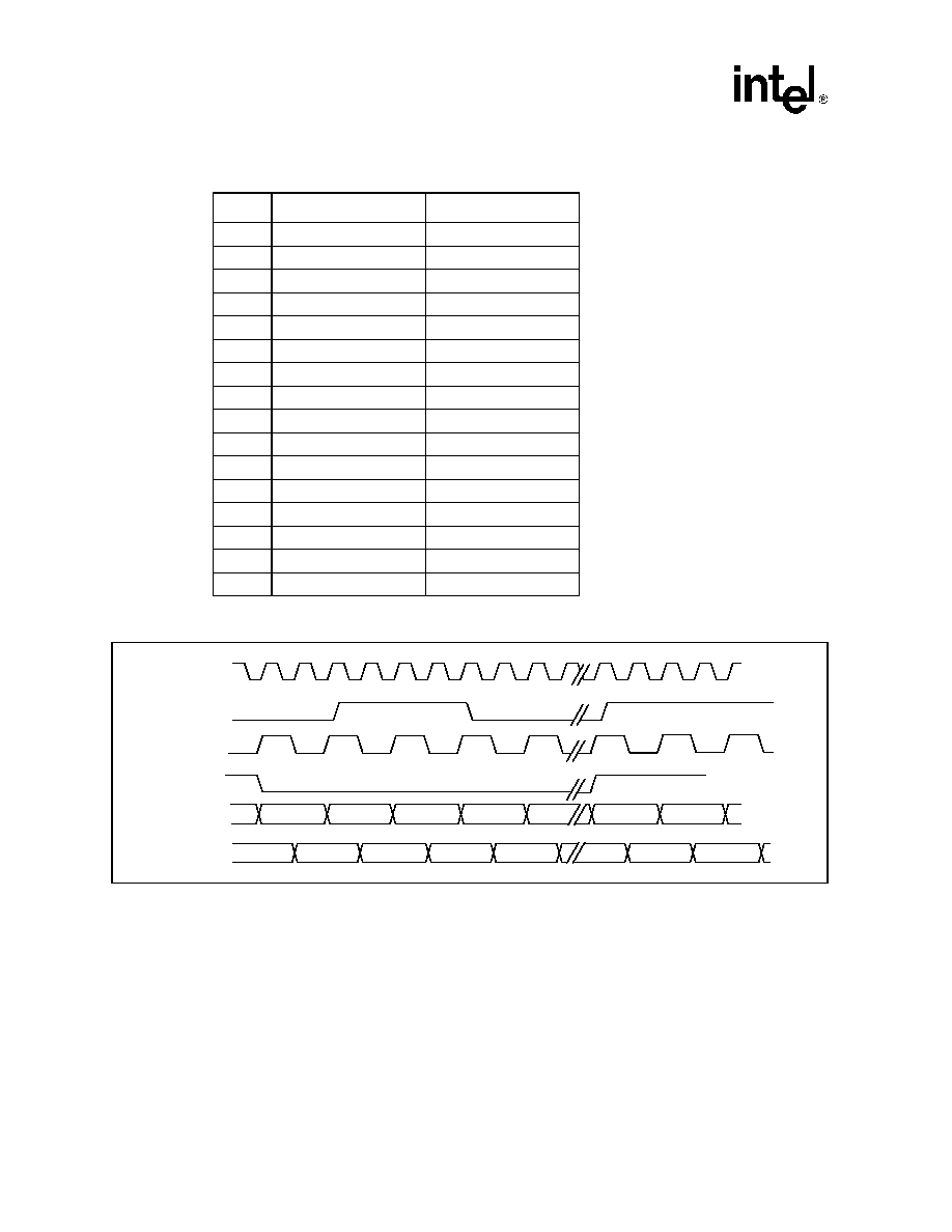
Figure 5. HDX/ACC Interface ≠ Relative Timing
CK37M
TCK4M
CK37M/2
AD0
AD1
DTR
FS
B1
B0
A15
A14
A13
B15
A1
A0

1168 Kbps HSDL Data Pump Chip Set -- SK70704/SK70707 or SK70708
Datasheet
19
5
shows the TDATA requirements for the framer interface through the activation sequence. Once
the ACTIVE Low-to-High transition occurs, the Data Pump becomes transparent. Therefore, the
HDSL framer must supply appropriate data to TDATA.
Table 5
summarizes this requirement.
The HDSL framer interface is subject to the following rules:
1. When frame sync is not present (LOSW is High), all RDATA bits are set to 1.
2. If frame sync is lost on both Data Pump-R1 and Data Pump-R2, both units will fall back on the
local reference frequency with ±32 ppm tolerance, and stuff bits will be injected in their
RDATA streams on every other frame.
1. If frame sync is lost on either Data Pump-R1 or Data Pump-R2, that unit can be made to fall
back on the REFCLK from the Data Pump-R which is still in frame sync, and stuff bits will be
injected in the RDATA stream on every other frame of the out-of-frame Data Pump-R.
2. If frame sync is lost on either Data Pump-C1 or Data Pump-C2, the receiver in each unit will
fall back on the reference clock with ±32 ppm or ±5 ppm tolerance, and inject stuff bits in the
RDATA stream on every other frame.
3. If either E1-R or E1-C loses sync or signal, it is assumed that the corresponding T1 receiver
will fall back on a local reference with ±32 ppm tolerance, and that transmit bit-stuffing
control will still be applied through the TFP signal from the HDSL framer.
4. The HDSL framer should provide TFP signal with a period of 6 ms ±
1
/
584
ms prior to an
activation request for the LTU Data Pump(s). The framer should provide a valid TFP after
power-up, before or immediately after LOS goes Low for the NTU Data Pump(s).
If the TFP signal from the HDSL framer is inactive (always High or unconnected), the Data
Pump will inject stuff bits in the TDATA stream in every other frame, although the Data Pump
will not be synchronized to the HDSL framer. When a new TFP is provided, the Data Pump
will immediately reset the transmit frame alignment, typically causing loss of alignment at the
other end.
5. A simultaneous RESET2 to all LTU Data Pumps which use a common REFCLK eliminates
phase shift between the ICLK outputs which may exist after power-up.
The ICLK outputs of all NTU Data Pumps may have an arbitrary phase difference even using a
common CK9M reference.
Table 5. HDSL Framer TDATA Requirements
Activation Process
TDATA
Framer
Data Pump
Overhead
Data
Idle
Activating
don't care
don't care
Idle
Active 1
live
all 1s
Active-R
Active 1
live
all 1s
Active-T
Active 1
live
live
Link Active
Active 1
live
live
Link Active
Active 2
live
live
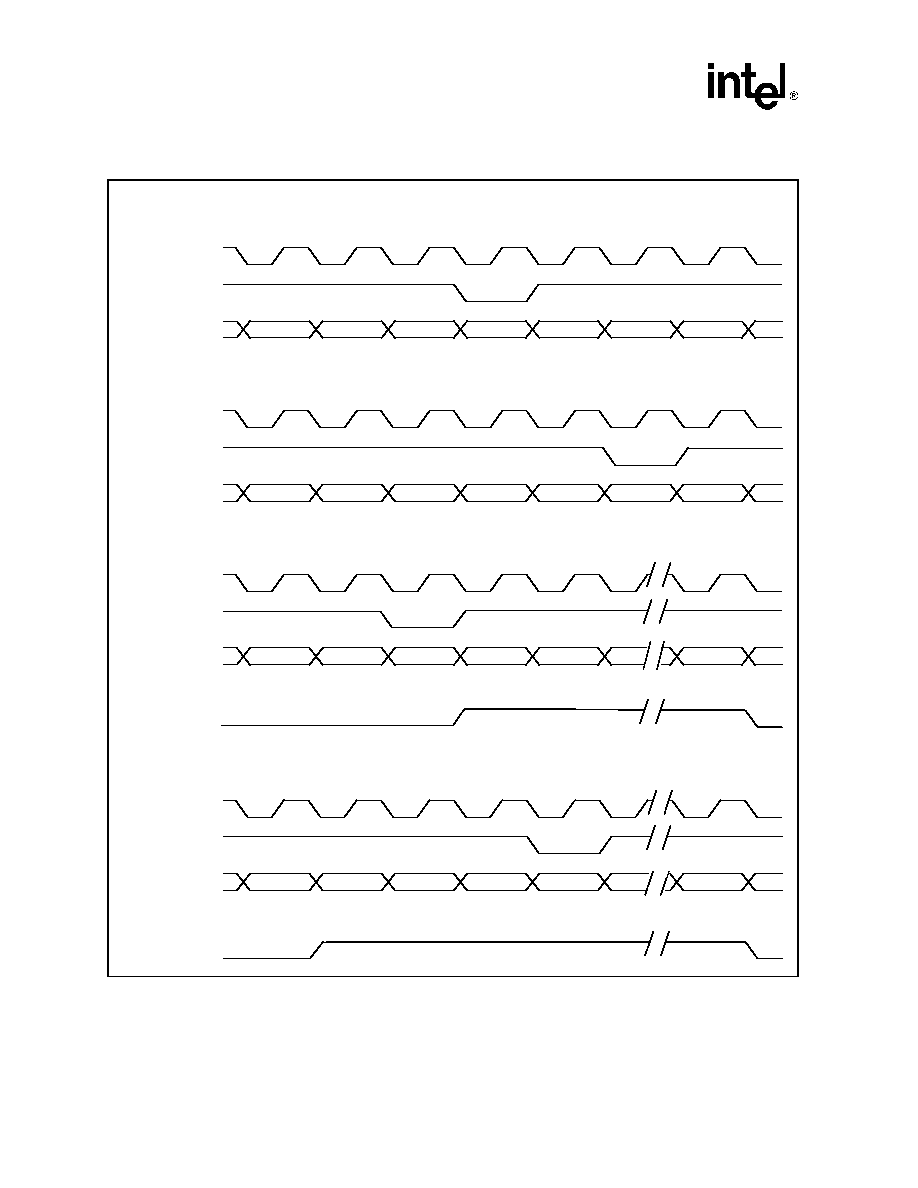
SK70704/SK70707 or SK70708 -- 1168 Kbps HSDL Data Pump Chip Set
20
Datasheet
Figure 6. HDX/ACC Framer Interface ≠ Relative Timing
A) Transmit Timing - Without Stuff Bits
C) Receive Timing - Without Stuff Bits
B) Transmit Timing - With Stuff Bits
D) Receive Timing - With Stuff Bits
b2
b7005
b7006
b7007
b7008
b7009
b7010
b1
ICLK
TFP
TDATA
b7003
b7004
b7005
b7006
b1
b2
b3
b4
ICLK
TFP
TDATA
b7004
b7005
b7006
b1
b2
b3
b14
b15
ICLK
RFP
RDATA
RFST
b7006
b7007
b7008
b7009
b7010
b1
b14
ICLK
RFP
RDATA
b15
RFST

1168 Kbps HSDL Data Pump Chip Set -- SK70704/SK70707 or SK70708
Datasheet
21
2.7
Microprocessor Interface (HDX)
Three primary control pins, CHIPSEL (Chip Select), READ and WRITE, execute the Software
Mode which also uses an interrupt output pin to report status changes. Four additional pins are used
for the parallel bus addressing and eight pins for data I/O. Refer to Test Specifications for
microprocessor interface timing in Software Mode. The following control pins are used during
register access.
2.7.1
Control Pins
Chip Select: The Chip Select (CHIPSEL) pin requires an active Low signal to enable Data Pump
read or write transfers over the data bus. To enable Hardware Mode hold this pin Low, along with
READ and WRITE.
Data Read: The Data Read pin (READ) requires an active Low pulse to enable a read transfer on
the data bus. When READ is pulled Low, the Data Pump data bus lines go from tristate to active
and output the data from the register addressed by ADDR0-ADDR3. To avoid reading data during
register updates, reads should be synchronized to the falling edge of FS. Alternatively, each read
should be repeated until the same data is read twice within one baud time.
Figure 7. Model for HDSL Data Pump and HDSL Framer Applications
Frequency Relationships
1. f
TCLK
(E1-C) = (E1-R); tolerance= ±32 ppm, even with loss of signal on E1-R.
2. f
TCLK
(E1-R)= (E1-C); tolerance= ±32 ppm, even with loss of signal on E1-C.
3. f
ICLK
(C)=
f
R
(C)
/
16
; tolerance= ±32 ppm if sourced by local crystal oscillator (stratum 4),
= ±5 ppm if sourced by office clock (stratum 3).
4.
f
ICLK
(R)= f
ICLK
(C) if loop is activated with receive frame sync acquired,
=
f
R
(R)
/
16
if receive sync is lost; tolerance = ±32 ppm (f
R
(R) =
18.688 MHz
).
=
f
R
(R)
/
8
if f
R
(R) =
9.344 MH
Z
.
LXP710
HDSL
Framer -
R
DP-R1
DP-R2
NTU
Local Xtal
Osc
TDATA
TFP
LOSW
ICLK
RDATA
RFP
RFST
REFCLK
TDATA
TFP
LOSW
ICLK
RDATA
RFP
RFST
To E1 I/F
(E1-R)
RPOS
RNEG
RCLK
TPOS
TNEG
TCLK
REFCLK
LXP710
HDSL
Framer -
C
DP-C1
DP-C2
LTU
TDATA
TFP
LOSW
ICLK
RDATA
RFP
RFST
TDATA
TFP
LOSW
ICLK
RDATA
RFP
RFST
To E1 I/F
(E1-C)
RPOS
RNEG
RCLK
TPOS
TNEG
TCLK
Rate
Synth
Local Xtal
Osc
REFCLK
fR (C)
REFCLK
CK9M
CK9M
f
R (R)

SK70704/SK70707 or SK70708 -- 1168 Kbps HSDL Data Pump Chip Set
22
Datasheet
Data Write: The Data Write pin (WRITE) requires an active Low pulse to enable a write transfer
on the data bus. Data transfer is triggered by the rising edge of the WRITE pulse. To ensure data is
written to the register addressed by ADDR0-ADDR3, valid data must be present on the HDX data
bus lines before WRITE goes High.
Interrupt: The Interrupt pin (INT) is an open drain output requiring an external pull-up resistor.
The INT output is pulled active Low when an internal interrupt condition occurs. INT is latched
and held until Main Status Register RD0 is read. An internal interruption results from a Low-to-
High transition in any of four status indicators: ACTIVE, LOSW, LOSWT or TEXP. Any transition
on LOS will also generate an interrupt. If an interrupt mask bit in register WR2 is set, any transition
of the corresponding status bit will not trigger the INT output.
2.7.2
Register Access
Write: To write to an HDX register, proceed as follows:
1. Drive CHIPSEL Low.
2. Drive an address (0000, 0010, or 0011) onto ADDR0-ADDR3.
3. Observe address setup time.
4. Set 8-bit input data word on D0-D7.
5. Pull WRITE Low, observing minimum pulse width.
6. Pull WRITE High, observing hold time for data and address lines.
Read: Procedures for reading the HDX registers vary according to which register is being read.
Accessing registers RD0, RD1, RD2, RD5 and RD6 is relatively simple. Reading registers RD3
and RD4 is more complex. Unless parallel port reads are synchronized with the falling edge of FS,
all read operations should be repeated until the same data is read twice within one baud time.
To read register RD0, RD1, RD2, RD5 or RD6 proceed as follows:
1. Drive CHIPSEL Low.
2. Drive the desired address onto ADDR0-ADDR3.
3. Pull READ Low, observing minimum pulse width.
4. Pull READ High to complete the read cycle.
Registers RD3 and RD4 hold the coefficient values from the DFE, EC, FFE and AGC as shown in
Table 9
. Register RD3 holds the lower byte value and register RD4 holds the upper byte value. To
reconstruct the complete 16-bit word, concatenate the least significant and most significant bytes.
To read registers RD3 and RD4 proceed as follows:
1. Select the desired coefficient by writing the appropriate code from
Table 9
to register WR3.
2. Enable the Coefficient Read Register by writing a 1 to bit b0 (CRD1) in register WR2.
3. Perform standard register read procedure listed in steps 1 through 6 above to read the lower
byte from RD3 and the upper byte from RD4.
4. Concatenate the RD3 and RD4 to obtain the complete 16-bit word.
1168 Kbps HSDL Data Pump Chip Set -- SK70704/SK70707 or SK70708
Datasheet
23
2.7.3
Registers
Three write registers and seven read registers are available to the user.
Table 6
lists these registers
and the following paragraphs describe them in more detail.
Some of the registers contain reserved bits. Software must deal correctly with reserved fields. For
reads, software must use appropriate masks to extract the defined bits and not rely on reserved bits
being any particular value. In some cases, software must program reserved bit positions to a
particular value. This value is defined in the individual bit descriptions.
After asserting the RESET1 and RESET2 signals, the Data Pump initializes its registers to the
default value.
2.7.3.1
WR0--Main Control Register
Address:
A3-0 = 0000
Default: 00h
Attributes:
Write Only
Control Register bits serve the same purpose in Software Mode as the like-named individual pins
in Hardware Mode.
Table 7
lists bit assignments for the WR0 register.
Table 6. Register Summary
ADDR
Write Registers
Read Registers
A3-A0
WR#
Name
Table
RD#
Name
Table
0000
WR0
Main Control
7
RD0
Main Status
10
0001
reserved
RD1
Receiver Gain Word
11
0010
WR2
Interrupt Mask
8
RD2
Noise Margin
12
0011
WR3
Read Coefficient Select
9
RD3
Coefficient Read Register (lower byte)
13
0100
reserved
RD4
Coefficient Read Register (upper byte)
13
0101
reserved
RD5
Activation Status
14
0110
reserved
RD6
Receiver AGC and FFE Step Gain
14
0111-1001
reserved
reserved
Table 7. Main Control Register WR0
Bit
Description
b7
Transmit Test Pattern Enable (TXTST). Set TXTST to 1 to enable isolated transmit pulse
generation. The time between pulses is 6 ms. TDATA controls the sign and TFP controls the
magnitude of the transmitted symbols according to the 2B1Q encoding rules. In the NTU
configuration when the TXTST mode is selected, the Data Pump may begin activation.
b6
Back-End Loop Back (BELB). In the Active State, set BELB to 1 to enable an internal, transparent
loopback of the HDX RDATA to TDATA and RFP to TFP.
b5
Front End Loop Back (FELB). In the LTU mode with the Data Pump in the Inactive State, set FELB
to 1 to enable an ACC front-end loopback. The Data Pump will begin activation and transmission on
the line, but will ignore any signal from the NTU instead synchronizing to its own transmit signal.
b4
Repeater Mode (RPTR). The RPTR bit is set to 1 and the LTU pin is pulled High to program the
Data Pump for operation on the side of the HDSL repeater driving the remote NTU. RPTR is set to 0
and the LTU pin is tied Low to program the Data Pump for operation on the side of the repeater
driven by the central office LTU.
SK70704/SK70707 or SK70708 -- 1168 Kbps HSDL Data Pump Chip Set
24
Datasheet
2.7.3.2
WR2--Interrupt Mask Register
Address: A3-0
=
0010
Default: 00h
Attributes:
Write Only
Table 8
shows the various interrupt masks provided in register WR2.
2.7.3.3
WR3--Read Coefficient Select Register
Address: A3-0
=
0011
Default: 00h
Attribute: Write
Only
Table 9
lists the bit maps used to select the coefficient read from the HDX.
b3
reserved. This bit must be set to 0.
b2
Insertion Loss Measurement Test (ILMT). Set ILMT to 1 to enable transmission of a scrambled all
ones insertion loss measurement test pattern. In the NTU configuration when the ILMT mode is
selected, the Data Pump may begin activation.
b1
Quiet Mode (QUIET). Set QUIET to 1 to force the Data Pump into the De-Activated State with the
transmitter silent. Setting QUIET to 0 will not cause the Data Pump to reactivate. In the NTU mode,
the Data Pump will not respond to an S0 signal from the LTU when QUIET is set to 1, but may
activate after QUIET is set to 0 even if the LTU transmission has already ceased.
b0
Activation Request (ACTREQ). In the LTU mode when the Data Pump is in the Inactive State and
Quiet is set to 0, setting the ACTREQ bit to 1 will initiate an activation sequence. Because ACTREQ
is a level- rather than an edge-triggered signal, it should be reset to 0 again within approximately 25
seconds to prevent the immediate start of another activation cycle if the current activation attempt
fails. If an activation attempt fails, the processor should allow the Data Pump to remain in the
Inactive State where the transmitter is silent for 32 seconds before generating another activation
request to allow the NTU to return to the Inactive State. It is possible to shorten this quiet period
following a failed activation by implementing additional algorithms described in the section entitled
"Activation State Machines."
Table 7. Main Control Register WR0 (Continued)
Bit
Description
Table 8. Interrupt Mask Register WR2
Bit
Description
b7-b6
Reserved. Must be set to 0.
b5
LOSMSK. 1=Masked. 0=Not Masked. Interrupt mask for the LOS condition.
b4
LSWTMSK. 1=Masked. 0=Not Masked. Interrupt mask for the LOSWT condition.
b3
LSWMSK. 1=Masked. 0=Not Masked. Interrupt mask for the LOSW condition.
b2
ACTMSK. 1=Masked. 0=Not Masked. Interrupt mask for the TEXP condition and the ACTIVE
condition.
b1
Reserved. Must be set to 0.
b0
CRD1. Enable coefficient read register. Used in conjunction with WR3 for reading coefficient values.
1168 Kbps HSDL Data Pump Chip Set -- SK70704/SK70707 or SK70708
Datasheet
25
2.7.3.4
RD0--Main Status Register
Address:
A3-0 = 0000
Default: xxh
(x=undefined)
Attribute: Read
Only
Status Register bits serve the same purpose in Software Mode as the like-named individual pins in
Hardware mode.
Table 10
lists the bit assignments in this register.
2.7.3.5
RD1--Receiver Gain Word Register
Address:
A3-0 = 0001
Default :
xxh (x=undefined)
Attributes:
Read Only
Table 9. Read Coefficient Select Register WR3
Hex Value
Selected Registers
Register Description
00-07
DFE1-DFE8
DFE coefficients
08-0F
EC1-EC8
Echo Cancellation
10-15
FFE1-FFE6
FFE coefficients 1-6
16-19
reserved
1A
AGC Tap
AGC Tap
1B-FF
reserved
Table 10. Main Status Register RD0
Bit
Active Description
b7
Timer Expiry (TEXP). Set to 1 to indicate 30-second timer expiration in the Active State.
∑
Causes interrupt on changing from 0 to 1; masked by ACTMSK = 1
∑
Latched event; reset on read, with persistence while in the Active State
b6
TIP/RING polarity reversed
(INVERT
). 0 = polarity reversal. Valid only in Active State.
b5
Change Of Frame Alignment (COFA). Indicates that re-acquisition of frame sync is in a different
position with respect to the last frame position. Does not cause interrupt. Latched event; reset on
read
b4
Loss Of Signal (NTU) (LOS). 1 = loss of line signal energy on entering Inactive State.
Loss of Signal Timer Expiration (LTU) (LOST). 1 = loss of signal for 1 second on entering
Inactive State.
∑
Causes interrupt on transitions from 0 to 1 or 1 to 0 that are masked by LOSMSK = 1
∑
LOS/LOST is not a latched event
b3
Reserved. This bit should be ignored.
b2
Loss of Sync Word Timer Expiry (LOSWT). Indicates two seconds of LOSW.
∑
Causes interrupt on changing from 0 to 1; masked when LSWTMSK = 1
∑
Latched event; reset on read; with persistence while in the Deactivated State
b1
Loss of Sync Word (LOSW).
∑
Causes interrupt on changing from 0 to 1; masked by LSWMSK = 1
∑
Latched event; reset on read; with persistence while in the Pending Deactivation State
b0
Active State (ACTIVE). 1 = Completion of layer 1 activation.
∑
Causes interrupt on changing from 0 to 1; masked by ACTMSK = 1
∑
Latched event; reset on read with persistence if still in the Active State
SK70704/SK70707 or SK70708 -- 1168 Kbps HSDL Data Pump Chip Set
26
Datasheet
The 8-bit word in this register is the eight most significant bits of the main FFE AGC tap, which,
along with the AGC and DAGC values (RD6), represent the receiver gain required to compensate
for line loss, and to normalize the receive 2B1Q pulses to a fixed threshold. Bit b7 (sign bit, always
0) is the MSB with bit b0 the LSB. The AGC tap value is determined as follows:
2.7.3.6
RD2--Noise Margin Register
Address:
A3-0 = 0010
Default: xxh
(x=undefined)
Attributes:
Read Only
The noise margin of the received signal is an input to the HDSL framer's Activation State
Machine. The noise margin must reach a threshold level before the HDSL framer can transition to
the fully Active State. The HDX provides a calculated, logarithmic noise margin value used by the
HDSL framer. This eight-bit word, stored in register RD2, is available every baud, although
updated only every 64 baud.
Table 12
shows the noise margin coding. To calculate the SNR, use
this equation:
SNR =Noise Margin + 21.5 dB
Error propagation in the DFE and de-scrambler may introduce some fractional errors in this
formula, however, the relationship between the SNR and the noise margin remains valid as long as
the noise follows a Gaussian distribution.
Since the average period of the calculation is very short (64 baud = 110 µs), the recommended
procedure for evaluating transmission quality is to average at least 1000 samples over a 110 ms
period.
Table 11. Receiver Gain Word Register
Bit
Description
b7-b0
FFE AGC Tap Value (eight most significant bits).
AGC Tap =
b
i
*2
i-6
i = 0
6
Table 12. Noise Margin Register RD2
Noise Margin Coding
1
MSB
LSB
Noise
Margin
b7
b6
b5
b4
b3
b2
b1
b0
0
0
1
1
0
1
0
1
+26.5
0
0
1
0
1
1
1
1
+23.5
0
0
1
0
1
0
1
1
+21.5
0
0
1
0
1
0
0
1
+20.5
0
0
1
0
0
1
1
1
+19.5
0
0
1
0
0
1
0
1
+18.5
1. Accuracy of noise margin is ± 1 dB
1168 Kbps HSDL Data Pump Chip Set -- SK70704/SK70707 or SK70708
Datasheet
27
2.7.3.7
RD3(LSB), RD4(MSB)--Coefficient Read Register
Address:
RD3 (A3-0 = 0011) RD4 (A3-0 = 0100)
Default:
xxh (x=undefined)
Attributes:
Read Only
Coefficient Read Word (read from the HDX) comes from the location configured in the Read
Coefficient Select Register (WR3, Address A3-0 = 0011). The HDX updates this word on the
rising edge of the receive clock, FS. Read register RD3 is the lower byte, and RD4 is the upper
byte.
0
0
1
0
0
1
0
0
+18.0
0
0
1
0
0
0
1
0
+17.0
0
0
1
0
0
0
0
0
+16.0
0
0
0
1
1
1
1
0
+15.0
0
0
0
1
1
1
0
0
+14.0
0
0
0
1
1
0
1
0
+13.0
0
0
0
1
1
0
0
0
+12.0
0
0
0
1
0
1
1
0
+11.0
0
0
0
1
0
1
0
0
+10.0
0
0
0
1
0
0
1
0
+9.0
0
0
0
1
0
0
0
0
+8.0
0
0
0
0
1
1
1
0
+7.0
0
0
0
0
1
1
0
0
+6.0
0
0
0
0
1
0
1
0
+5.0
0
0
0
0
1
0
0
0
+4.0
0
0
0
0
0
1
1
0
+3.0
0
0
0
0
0
1
0
0
+2.0
0
0
0
0
0
0
1
0
+1.0
0
0
0
0
0
0
0
0
0.0
1
1
1
1
1
1
1
0
-1.0
1
1
1
1
1
1
0
0
-2.0
1
1
1
1
1
0
1
0
-3.0
1
1
1
1
1
0
0
0
-4.0
1
1
1
1
0
1
1
0
-5.0
1
1
1
1
0
1
0
0
-6.0
Table 12. Noise Margin Register RD2 (Continued)
Noise Margin Coding
1
MSB
LSB
Noise
Margin
b7
b6
b5
b4
b3
b2
b1
b0
1. Accuracy of noise margin is ± 1 dB
SK70704/SK70707 or SK70708 -- 1168 Kbps HSDL Data Pump Chip Set
28
Datasheet
2.7.3.8
RD5--Activation Status Register
Address: A3-0
=
0101
Default: xxh
(x=undefined)
Attributes: Read
Only
The ACT bits indicate the current state of the HDX transceiver during the Activating State as listed
in
Table 14
. (For any state other than the Activating State, the ACT bits will be "0000".)
2.7.3.9
RD6--Receive Step Gain Register
Address:
A3-0 = 0110
Default: xxh
(x=undefined)
Attributes:
Read Only
This 8-bit register represents AGC and FFE gain coefficients (GAGC and GFFE, respectively). Bit
assignments are listed in
Table 15
. The approximate line loss (L
L
) can be determined using these
values in the following equation:
L
L
= 20log
10
(GFFE
*
AGC tap) + GAGC + 28 dB
GFFE corresponds to DAGC in the HDX and GAGC is from the ACC. Bits ST0-ST2 indicate the
Data Pump activation states as shown in
Figure 8
and
Figure 10
and Table
Table 16
.
Table 13. Coefficient Read Register
Bit
Description
b7-b0
Coefficient Word Value. RD3 contains the lower byte; RD4 the upper byte.
Table 14. Activation Status Register RD5
ACT Bits 3-0
State in
LTU Mode
State in
NTU Mode
0000
Inactive
Inactive
0001
Pre-AGC
Wait
0010
Pre-EC
AAGC
0011
SIGDET
EC
0100
AAGC
PLL1
0101
EC
PLL2
0110
PLL
4LVLDET
0111
4LVLDET
FRMDET
1000
FRMDET
≠

1168 Kbps HSDL Data Pump Chip Set -- SK70704/SK70707 or SK70708
Datasheet
29
2.8
Activation State Machines
The Data Pump Activation/Start-Up circuitry is compatible with ETSI ETR-152. Full LTU
activation is partitioned between the Data Pump and the framer.
Figure 8
represents the LTU Data
Pump Activation State Machine, and
Figure 9
shows the LTU framer activation state machine.
Figure 10
and
Figure 11
present the corresponding NTU state machines.
Table 16
lays out the
correspondence between the Data Pump and Framer state machines. In Software Mode, the STn
bits in Read Register 6 (ADDR 0110) show the current status of the state machine.
2.8.1
LTU Data Pump Activation
When the LTU Data Pump is powered up and reset is applied, the chip is in the Inactive State as
shown at the top of
Figure 8
. Starting at the Inactive State, the device progresses in a clockwise
direction through the Activating, Active-1, Active-2, Pending De-Activation and De-Activated
States.
In the hardware mode when the Data Pump is in the Inactive State and the QUIET pin is Low, a
Low-to-High transition on the ACTREQ pin initiates activation of the link. In the software mode
when the Data Pump is in the Inactive State and the QUIET bit is set to 0, setting the ACTREQ bit
to 1 initiates activation of the link. Because the ACTREQ control bit is level sensing, it should be
set to 1 and then reset to 0 again within 25 seconds to generate a single activation request.
Table 15. Receiver AGC and FFE Step Gain Register RD6
Bit
Description
b7
Data Pump Activation State≠bit 2 (ST2).
b6
Data Pump Activation State≠bit 1 (ST1).
b5-b4
Digital Gain Word≠bit 1 and 0 (GFFE1,0).
Bits <5:4>GFFE Value
00
2
0
= 1
01
2
1
= 2
10
2
2
= 4
11
2
3
= 8
b3
Data Pump Activation State≠bit 0 (ST0).
b2-b0
Analog Gain Word≠bit 2,1 and 0 (GAGC2,1,0).
Bits <2:0>GAGC Value (db)
000
-12
001
-10
010
-8
011
-6
100
-4
101
-2
110
0
111
+2
SK70704/SK70707 or SK70708 -- 1168 Kbps HSDL Data Pump Chip Set
30
Datasheet
During the Activating State, the echo canceller, equalizer and timing recovery circuits are all
adapting during the simultaneous transmission and reception of the framed, scrambled-ones data
transmitted as a two-level code (S0) or as the four-level code (S1). If the receive frame sync word
is not detected in two consecutive frames within 30 seconds, the timer expires and the device
moves to the De-Activated State and ceases transmission. It will then immediately transition to the
Inactive State (setting LOST regardless of whether NTU transmission has ceased). Another
activation request should not be generated for 32 seconds allowing the NTU to timeout, detect LOS
and move from the De-Activated to the Inactive State. In microprocessor-based systems, this time
may be shortened by implementing a processor routine to reset the NTU Data Pumps which are in
the Activating State when no LTU signal is present.
Successful detection of the sync word drives the State machine to the Active-1 State. This is
indicated by a 0-to-1 transition of the ACTIVE bit (Software Mode). If the LTU Data Pump
remains locked to the sync word until the Activation Timer expires, the device transitions to the
Active-2 (fully active) State. If sync is lost, as indicated by a 0-to-1 transition on LOSW, the LTU
Data Pump transitions to the Pending De-Activation State.
In Pending De-Activation, the LTU Data Pump progresses to the De-Activated and Inactive States
with the expiration of the respective timers. If the sync word is detected before the LOSW timer
expires, the LTU Data Pump returns to either Active 1 or Active-2. The LTU Data Pump returns to
whichever state it occupied before transitioning to Pending De-Activation.
The LTU Data Pump will exit the Active-2 State in one of two ways. A Low-to-High transition on
the QUIET pin (Hardware Mode) or the QUIET bit (Software Mode), forces the LTU Data Pump
directly to the De-Activated State. The only other means of exiting the Active State is through a
loss of receive sync word (LOSW). LOSW is set when six consecutive frames occur without a sync
word match. The LOSW event puts the LTU Data Pump into the Pending De-Activation State.
The LTU Data Pump remains in the Pending De-Activation State for a maximum of two seconds. If
a sync word is detected within two seconds after the LOSW event, the LTU Data Pump re-enters
the Active State. If the LOSW condition exceeds two seconds, an LOSWT event occurs which
sends the chip to the De-Activated State. When the De-Activated State is reached from Pending
De-Activation, the LTU Data Pump returns to the Inactive State and declares LOST when it detects
no signal from the NTU for one second. The Data Pump should remain in the Inactive State for 15
seconds before another activation attempt.
Table 16. Data Pump/Framer Activation State Machine Correspondences
ST2
ST1
ST0
Data Pump State
Framer State
0
0
0
Inactive
Idle
0
0
1
Activating ≠
30 sec timer
running
Idle
0
1
0
Active ≠ 30 sec
timer running
(Active-1)
1
Idle, Active-R or
Active-T, or Link
Active
0
1
1
Active ≠ 30 sec
timer expired
(Active-2)
1
Link Active
1. The data pump samples the TDATA input for all transmit data
except the 14 sync bits at the start of each frame during
states 010, 011 and 100.

1168 Kbps HSDL Data Pump Chip Set -- SK70704/SK70707 or SK70708
Datasheet
31
2.8.2
LTU Framer Activation
Figure 9
shows the activation state machine for the LTU HDSL framer. Transition to the Link
Active stage from the Idle stage (upper left) requires successful exchange of a pair of indicator bits,
indc and indr ("INDC" and "INDR" are internal status signals within the HDSL framer; "indc"
and "indr" are bits in the overhead channel). The LTU device transmits the indc bit, and the NTU
device transmits the indr bit. The overhead frame carries these indicator bits during transmission
of the S1 training pattern.
Figure 9
illustrates the two partially active states (Active-R and Active-T) which may serve as
transitions between the Idle and Link Active States. If the LTU device reaches the SNR threshold,
its framer sets the INDC bit and the device transitions to the Active-R State. If the NTU device
reaches the SNR threshold, it will transmit the indr bit to the LTU. The LTU will then transition to
the Active-T State. From either of the partially Active States, the devices transition to the full Link
Active State only with both Indication bits set.
Upon entering the Active States (Active-R, Active-T or Link Active), the chip will open up the full
duplex communication link with the NTU. Only the Active and Pending De-Activation States
allow full payload transmission. In all states except Active-1 and Active-2, the RDATA output is
clamped High.
1
0
0
Pending
De-Activation
1
Link Active or
Active-R or
Active-T
1
0
1
De-Activated Idle
1
1
0
unused
unused
1
1
1
unused
unused
Table 16. Data Pump/Framer Activation State Machine Correspondences (Continued)
ST2
ST1
ST0
Data Pump State
Framer State
1. The data pump samples the TDATA input for all transmit data
except the 14 sync bits at the start of each frame during
states 010, 011 and 100.
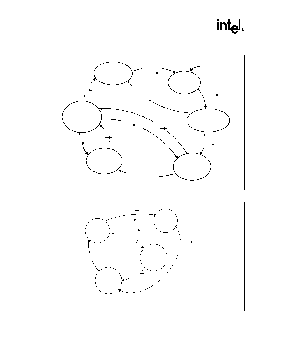
SK70704/SK70707 or SK70708 -- 1168 Kbps HSDL Data Pump Chip Set
32
Datasheet
Figure 8. LTU Data Pump Activation State Machine
Figure 9. LTU HDSL Framer Activation State Machine
De-Activated
Txmitter silent
(1, 0, 1)
LOST
0 1
DP Activating
Txmitting S0 or S1
(0, 0, 1)
Active 1
Txmitting S1 or
2B1Q Live data
(0, 1, 0)
LOSW
1 0
Active 2
Txmitting 2B1Q
Live data
(0, 1, 1)
Actvation
Timer
Expiration
LOSW
1 0
LOSW
0 1
LOSW
1 0
LOSW
0 1
Activation
Timer
Expiration
LOSWT
0 1
ACTREQ
0 1
Pending
De-Activation
Txmitting 2B1Q
Data (1, 0, 0)
Inactive
Txmitter silent
(0, 0, 0)
Power On
NOTE: (n, n, n) indicates the status of bits ST2, ST1 and ST0 respectively.
Idle
Active-R
Active-T
Link
Active
ACTIVE: 0 1
&
indr: 0 1
LOSWT = 1
INDC: 0 1
or
Timer Expiration
indr: 0 1
or
Timer Expiration
ACTIVE: 0 1
&
INDC: 0 1

1168 Kbps HSDL Data Pump Chip Set -- SK70704/SK70707 or SK70708
Datasheet
33
2.8.3
NTU Data Pump Activation
Figure 10
and
Figure 11
represent the NTU Data Pump Activation State Machine and the NTU
HDSL Framer State Machine. The activation state machines for NTU and LTU devices are similar.
Both Data Pump machines start at the Inactive State and progress clockwise through the
Activating, Active-1, Active-2, Pending De-Activation, and De-Activated States. One difference
between them is in the initial condition required to exit from the Inactive State. The LTU Data
Pump responds to the Activation Request (ACTREQ) signal. The NTU device responds only to the
presence of signal energy on the link. Thus, only an active LTU device can bring up the link. Once
the LTU begins transmitting, the NTU device will automatically activate and attempt
synchronization.
The other difference between the Data Pump state machines is the impetus for the change from the
De-Activated to the Inactive State. In the LTU Data Pump, expiration of a one-second loss of signal
timer (LOST) causes the transition. In the NTU the transition occurs immediately on Loss of Signal
(LOS).
2.8.4
NTU Framer Activation
The HDSL framer activation state machines for LTU and NTU are also similar. The difference is in
the indicator bits which cause the transition to either the Active-T or Active-R State. On the NTU
side, the INDR bit causes the transition to the Active-R State, and the indc bit causes the transition
to the Active-T State. From either partially active state, receipt of the remaining indicator bit or
timer expiry causes the transition to the full Link Active State.
2.8.5
HDSL Synchronization State Machine
Figure 12
shows the HDSL Synchronization State Machine incorporated in the HDX. It applies to
both LTU and NTU devices.
Table 17
lists the correspondence between the Synchronization states
and Activation states. The Sync state machine is clocked by the receive signal framing. Starting at
the initial Out-of-Sync condition (State 0), the device progresses in a clockwise direction through
State 1 until Sync is declared in State 2. Two consecutive frame sync word matches are required to
achieve synchronization.
Once the In-Sync condition is declared, six consecutive frame sync mismatches will cause the
device to transition through States 3 through 7 and declare an Out-of-Sync condition in State 8.
From State 8, the device will return either to State 2 or to State 0. If the 2-second timer expires
without re-establishing frame sync (LOSWT = 1) or if the receive signal is lost entirely (LOS = 1),
the device returns directly to State 0.
If frame sync is re-established, the device will return to the In-Sync condition (State 2) through
State 9 if two consecutive frames are received without any change of frame alignment (COFA = 0).
If a change of frame alignment does occur (COFA = 1), two consecutive matches are required to
transition through State 10 back to State 2.
Table 17. Activation ≠ Synchronization
Activation State
Synchronization States
Inactive
State 0
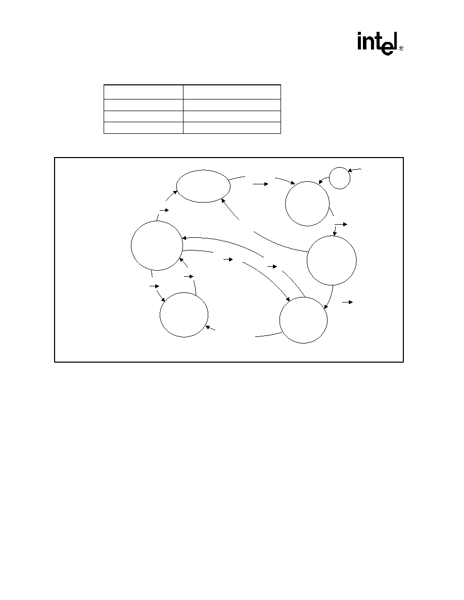
SK70704/SK70707 or SK70708 -- 1168 Kbps HSDL Data Pump Chip Set
34
Datasheet
Activating
State 1
Active
States 2, 3, 4, 5, 6, and 7
Pending De-Activation
States 8, 9, and 10
Figure 10. NTU Data Pump Activation State Machine
Table 17. Activation ≠ Synchronization
Activation State
Synchronization States
De-Activated
Txmitter silent
(1, 0, 1)
Inactive
Txmitter silent
(0, 0, 0)
LOS
0 1
Power
On
DP Activating
Txmitting S0 or
S1
(0, 0, 1)
Active 1
Txmitting S1 or
2B1Q Live data
(0, 1, 0)
Active 2
Txmitting 2B1Q
Live data
(0, 1, 1)
Activation
Timer
Expiration
Pending
De-Activation
Txmitting 2B1Q
Data (1, 0, 0)
LOSW
1 0
LOSW
0 1
LOSW
1 0
LOSW
0 1
Activation Timer
Expiration
LOSWT
0 1
1-sec
Timer
LOSW
1 0
LOS
1 0
NOTE: (n, n, n) indicates the status of bits ST2, ST1 and ST0 respectively.
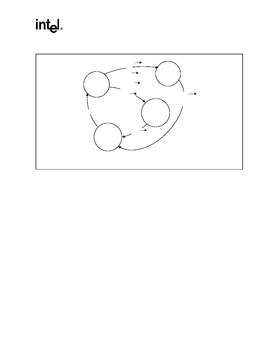
1168 Kbps HSDL Data Pump Chip Set -- SK70704/SK70707 or SK70708
Datasheet
35
Figure 11. NTU HDSL Framer Activation State Machine
Idle
Active-R
Active-T
Link
Active
LOSWT = 1
INDR: 0 1
or
Timer Expiration
ACTIVE: 0 1
&
indc: 0 1
ACTIVE: 0 1
&
INDR: 0 1
indc: 0 1
or
Timer Expiration

SK70704/SK70707 or SK70708 -- 1168 Kbps HSDL Data Pump Chip Set
36
Datasheet
Figure 12. HDSL Synchronization State Machine
NOTES:
1. "Sync" = Frame Sync Word Match. "No Sync" = Frame Sync Word Mismatch.
2. A 0-to-1 transition on QUIET will set the Sync State Machine from any State to State 0.
3. Expiration of the Activation Timer will set the Sync State Machine from State 1 to State 0.
Sync
No Sync
Initial
"Out-of-Sync"
State 0
ACTIVE = 0
LOSW = 0
LOS = 1
1
No Sync
Out of Sync
State 8
ACTIVE = 0
LOSW = 1
LOS = 0
No Sync
9
Sync with No
Change Of
Frame
Alignment
No Sync
No Sync
7
6
No Sync
5
No Sync
4
No Sync
3
No Sync
In Sync
State 2
ACTIVE =1
LOSW = 0
LOS = 0
Sync
No Sync
LOS = 1
or
LOSWT = 1
Sync
Sync
Sync
10
COFA = 1
Sync with Change
Of Frame
Alignment
Sync
COFA = 1
Sync
(COFA = 0)
No Sync

1168 Kbps HSDL Data Pump Chip Set -- SK70704/SK70707 or SK70708
Datasheet
37
3.0
Application Information
3.1
HDSL Framer State Machine Design
There are two issues that impact implementation of the HDSL Framer Activation State machines
for both LTU and NTU devices. These issues relate to the data transparency characteristics of the
Data Pump as follows:
1. Once the ACTIVE 0-to-1 transition occurs, the Data Pump becomes transparent. Therefore,
the HDSL framer must put appropriate data in TDATA.
Table 5
summarizes this requirement.
2. The link indicator bits (indc and indr) must stabilize before the device makes the transition
from the Idle to the Active-T State. Thus, the HDSL framer design may detect 6 consecutive
matches for the indication bit transition. This is particularly important for non-CSA loops
where a lower SNR may be experienced.
3.2
PCB Layout
The following are general considerations for PCB layout using the HDSL Data Pump chip set:
∑
Refer to
Figure 13
,
Figure 14
,
Figure 15
and
Figure 16
, and
Table 18
∑
Keep all shaded components close to the pins they connect to
∑
Use a four-layer or more PCB layout, with embedded power and ground planes
∑
Break up the power and ground planes into the following regions, and tie these regions
together at the common point where power connects to the circuit:
-- Digital Region
-- Analog Region
-- VCO subregion
-- ACC, Line I/F, and IBIAS subregion
∑
Use larger feedthroughs ("vias") and tracks for connecting the power and ground planes to the
power and ground pins of the ICs than for signal connections
∑
Place the decoupling capacitors right at the feed-through power/ground plane ties, or on the
tracks to the IC power/ground pins as close to the pins as possible
∑
On the User Interface Connector, route digital signals to avoid proximity to the TIP, RING,
and CT lines
∑
Provide at least 100 µF or more of bulk power supply decoupling at the point where power is
connected to the Data Pump circuit
3.2.1
User Interface
The REFCLK and CK9M signals are sensitive to capacitive loading and rise time. Keep
the rise time (from 10%-90%) for these signals less than 5 ns.

SK70704/SK70707 or SK70708 -- 1168 Kbps HSDL Data Pump Chip Set
38
Datasheet
3.2.2
Digital Section
∑
Keep all digital traces separated from the analog region of the Data Pump layout
∑
Provide high frequency decoupling capacitors (0.01 µF ceramic or monolithic) around the
HDX as shown in
Figure 14
and
Figure 15
∑
The capacitor on the HDX VCC1 pin (pin 1) should be on the IC side of the diode
∑
It is possible to replace the NAND gate (shown in
Figure 15
) with an AND gate
3.2.3
Analog Section
The analog section of the PCB consists of the following subsections:
1. ACC and power supply decoupling capacitors.
2. Bias Current Generator.
3. Voltage Controlled Crystal Oscillator.
4. Line Interface Circuit.
-- Route digital signals AD0, AD1, FS, DTR, TSGN, TMAG, TCK4M, and AGCKIK on the
solder side of the PCB
-- Route all analog signals on the component side as much as possible
-- Route the following signal pairs as adjacent traces, but keep the pairs separated from each
other as much as possible:
TTIP/TRING
BTIP/BRING
RTIP/RRING
-- To maximize high voltage isolation, do not run the analog ground plane under the
transformer line side

1168 Kbps HSDL Data Pump Chip Set -- SK70704/SK70707 or SK70708
Datasheet
39
Figure 13. PCB Layout Guidelines
R5
Y1
1
2
3
4
5
6
7
8
9
10
11
12 13
14 15 16 17 18
19
20
21
22
23
24
25
26
27
28
ACC
SK70704
C7
R1
C2
FS
DT
R
CK
25M
AG
C
K
IK
AD
1
AD
0
TC
K
3
M
G
ND3
TS
GN
TM
A
G
6
1 44
18
19 20 21
22
23 24 25 26 27
HDX
SK70708
17
7
40
39
30
28
R
ESET
2
1
8
9
10
11
25
26
27
28 29
30
31 32
33
34 35
36 37
38
39 40
41 42
43
44
45
59
60
61
68
HDX
SK70707
n/
c
n/
c
n/
c
n/
c
n/
c
n/
c
n/
c
C1
R6
R9
R1
0
R7
R8
R1
2
R1
3
Digital GND and VCC
Planes
Analog GND and VCC
Planes
DVCC
TVCC
DGND
TGND
No GND and VCC
Planes this side
RV
CC
RT
I
P
RRI
NG
RG
ND
BT
IP
BR
IN
G
n/
c
D2
D1
R4
C4
C3
R3
R2
C5
C6
R11
TIP
RING
VCC
GND
NOTE: The VCC and GND planes for Digital and Analog sides should be
connected at a single point.

SK70704/SK70707 or SK70708 -- 1168 Kbps HSDL Data Pump Chip Set
40
Datasheet
Figure 14. Typical Support Circuitry for LTU Applications
Table 18. Components for Suggested Circuitry (Figure 14 and Figure 15)
Ref
Description
Ref
Description
Ref
Description
C1, 9, 10
0.01
µ
F, ceramic, 10%
R1
10.0 k
, 1%
R12, 13
5.6
, line feed fuse resistor
(ALFR-2-5.6-1 IRC)
C2
33
µ
F, electrolytic, 20% low
leakage
5 µ
A @ 25∞ C
R2
35.7 k
, 1%
R3, 4
20.0 k
, 1%
D1, 2
Varicap diode (Motorola MV209)
C3, 4
1000 pF, ceramic, 20%
R5, 6
301
, 1%
D3
Silicon rectifier diode (1N4001)
C5, 6
470 pF, COG or mica, 10%
R7, 8
1
18.2
, 1%
Y1
37.376 MHz crystal
(Hy-Q International 81256/1)
C7, 11-13
0.1
µ
F, ceramic, 10%
R9, 10
604
, 1%
C8
100
µ
F, electrolytic, 20%
R11
1.43 k
, 1%
T1
1:1.8 (Midcom 671-7671 or
Pulse Engineering PE-68650)
R14
10.0 k
, 1%
1. R7, R8 should be 20
, when R12 and R13 (the 5.6
fuse links) are not used.
U1
SK70707
HDX
(SK70708
pins in
brackets)
V
CC1
G
ND1
G
ND2
V
CC2
G
ND3
RE
FCLK
CK
9M
LT
U
RFP
9 [7]
RFST
14 [10]
RDATA
8
ICLK
21 [17]
TFP
16 [12]
TDATA
15 [11]
4
ADDR0
5
6
7 [9]
54 [35]
READ
53 [34]
WRITE
52 [33]
CHIPSEL
51 [32]
INT
D0-D7
55,61-67
[36-43]
TSGN
40 [27]
TMAG
39 [26]
TCK4M
38 [25]
AGCKIK
AD1
37 [24]
AD0
36 [23]
FS
35 [22]
DTR
1
CK37M
34 [21]
33 [20]
32 [19]
RESET1
50 [31]
RESET2
23 [18]
ADDR1
ADDR2
ADDR3
2
3
68
[44]
42
[28]
17
[13]
18
[14]
20
[16]
U2
SK70704
ACC
TSGN
TMAG
TCK4M
AGCKIK
AD1
AD0
FS
DTR
CK37M
TV
CC
TGND
DV
CC
DG
ND
RV
CC
23
20
24
6
12
RG
ND
15
25
26
27
28
1
2
3
4
5
13
14
16
17
21
22
11
RTIP
RRING
BTIP
BRING
TTIP
TRING
IBIAS
VPLL
XI
XO
PG
N
D
9
8
7
10
Y1
R11
C5
R7
R8
R10
C6
R5
R6
C3
C4
C1
R4
R3
R12
R13
+5V
+
C8
PROCESSOR
I/F
HDSL
FRAMER
I/F
T1
1:1.8
2
4
6
10
RESET-
+5V
+5V
R2
C7
R9
D2
D1
R1
C2
D3*
C10
C9
C12
C13
C11
G
ND4
47
[n/c]
CMOS CLOCK
OSCILLATOR
18.688 MHZ
(± 32 PPM)
+5V
n/c
19
[15]
n/c
NOTES:
1. Diode D3 is optional.
2. The HDX and ACC should have independent ground planes connected at a single point near pin 5 of the ACC.
1168 Kbps HSDL Data Pump Chip Set -- SK70704/SK70707 or SK70708
Datasheet
41
Table 19. Transformer Specifications
(Figure 14 and Figure 15, Reference T1)
Measure
Value
Tolerance
Turns Ratio (IC:Line)
1:1.8
±1%
Secondary Inductance (Line
Side)
2.05 mH
±6%
Leakage Inductance
50
µ
H
Interwinding Capacitance
60 pF
THD
-70 dB
Longitudinal Balance
50 dB
5-292 kHz
Return Loss
20 dB
40-200 kHz
Isolation
2000 VRMS
Primary DC Resistance
2.0
Secondary DC Resistance
4.0
Operating Temperature
-40 to +85 ∞C
Table 20. Crystal Specifications
(Figure 14 and Figure 15, Reference Y1)
Measure
Value
Tolerance
Calibration Frequency
37.376 MHz
@ C
L
= 20 pF
0 to +40 ppm
Mode
Fundamental,
Parallel
Resonance
Pullability
(C
L
= 24 pF
’
16 pF)
+160 ppm
Operating Temperature
-40 to +85 ∞C
Temperature Drift
±30 ppm
Aging Drift
5 ppm/year
Series Resistance
15
Drive Level
0.5 mW
Holder
HC-49
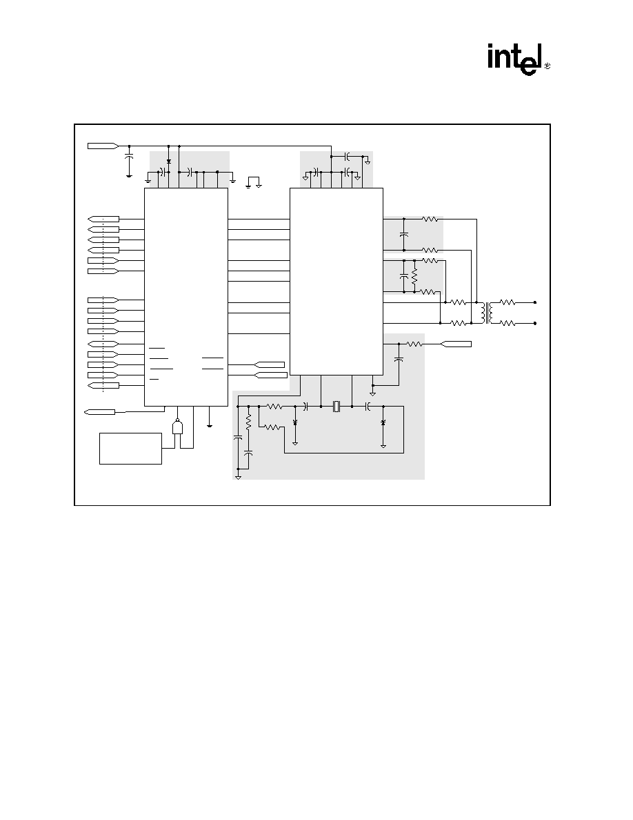
SK70704/SK70707 or SK70708 -- 1168 Kbps HSDL Data Pump Chip Set
42
Datasheet
Figure 15. Typical Support Circuitry for NTU Applications
U1
SK70707
HDX
(SK70708
pins in
brackets)
V
CC1
G
ND1
G
ND2
V
CC2
G
ND3
RE
FCL
K
CK
9
M
LT
U
RFP
9 [7]
RFST
14 [10]
RDATA
8
ICLK
21 [17]
TFP
16 [12]
TDATA
15 [11]
4
ADDR0
5
6
7 [9]
54 [35]
READ
53 [34]
WRITE
52 [33]
CHIPSEL
51 [32]
INT
D0-D7
55,61-67
[36-43]
TSGN
40 [27]
TMAG
39 [26]
TCK4M
38 [25]
AGCKIK
AD1
37 [24]
AD0
36 [23]
FS
35 [22]
DTR
1
CK37M
34 [21]
33 [20]
32 [19]
RESET1
50 [31]
RESET2
23 [18]
ADDR1
ADDR2
ADDR3
2
3
68
[44]
42
[28]
17
[13]
18
[14]
20
[16]
U2
SK70704
ACC
TSGN
TMAG
TCK4M
AGCKIK
AD1
AD0
FS
DTR
CK37M
TV
CC
TG
ND
DV
CC
DG
ND
RV
CC
23
20
24
6
12
RG
ND
15
25
26
27
28
1
2
3
4
5
13
14
16
17
21
22
11
RTIP
RRING
BTIP
BRING
TTIP
TRING
IBIAS
VPLL
XI
XO
PGN
D
9
8
7
10
Y1
R11
C5
R7
R8
R10
C6
R5
R6
C3
C4
C1
R4
R3
R12
R13
+5V
+
C8
PROCESSOR
I/F
HDSL
FRAMER
I/F
T1
1:1.8
2
4
6
10
RESET-
+5V
+5V
R2
C7
R9
D2
D1
R1
C2
D3*
C10
C9
C12
C13
C11
G
ND4
47
[n/c]
CMOS CLOCK
OSCILLATOR
9.344 or 18.688 MHZ
(± 32 PPM)
CK
9
M
19
[15]
NOTES:
1. Diode D3 is optional.
2. The HDX and ACC should have independent ground planes connected at a single point near pin 5 of the ACC.
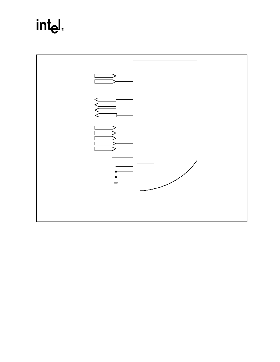
1168 Kbps HSDL Data Pump Chip Set -- SK70704/SK70707 or SK70708
Datasheet
43
Figure 16. SK70707/SK70708 HDX Control and Status Signals (Hardware Mode)
U1
SK70707/
SK70708
HDX
ACTREQ
5 [5]
QUIET
4 [4]
ACTVNG
7 [9]
TEXP
51 [32]
LOSWT
63 [37]
55 [36]
LOST/LOS
62 [38]
67 [43]
61 [39]
65 [41]
READ
52 [33]
WRITE
53 [34]
CHIPSEL
54 [35]
RCLKU
FELB
64 [40]
ILMT
TXTST
RPTR
BELB
66 [42]
n/c
NOTES:
1. This figure illustrates the HDX control and status signals in Hardware Mode. All other HDX and ACC signals are
connected as shown in
Figure 14
and
Figure 15
.
2. Pin numbers for SK70708 are shown in brackets [ ]. Pin numbers outside brackets are for SK70707.

SK70704/SK70707 or SK70708 -- 1168 Kbps HSDL Data Pump Chip Set
44
Datasheet
4.0
Test Specifications
Note:
The minimum and maximum values in
Table 21
through
Table 31
and
Figure 17
through
Figure 23
represent the performance specifications of the Data Pump and are guaranteed by test, except
where noted by design.
Table 21. ACC Absolute Maximum Ratings
Parameter
Symbol
Min
Max
Units
Supply voltage
1
reference to ground
2
TVCC, RVCC, DVCC
-0.3
+6.0
V
Input voltage
2, 3
, any input pin
TVCC, RVCC, DVCC
- 0.3V
VCC + 0.3
V
Continuous output current, any output pin
≠
≠
±25
mA
Storage temperature
T
STOR
-65
+150
∞C
Caution: Operations at the limits shown may result in permanent damage to the Analog Core Chip.
Normal operation at these limits is neither implied nor guaranteed.
NOTES:
1. No supply input may have a maximum potential of more than ±0.3 V from any other supply input.
2. TGND = 0V; RGND = 0V; DGND = 0V.
3. TVCC = RVCC = DVCC = VCC.
Table 22. ACC Recommended Operating Conditions
Parameter
Symbol
Min
Typ
Max
Units
DC supply
TVCC, DVCC,
RVCC
4.75
5.0
5.25
V
Ambient operating temperature
T
A
-40
+25
+85
∞C
Table 23. ACC DC Electrical Characteristics (Over Recommended Range)
Parameter
Sym
Min
Typ
1
Max
Unit
Test Conditions
Supply current (full operation)
I
CC
≠
102
137
mA
83
resistor across TTIP and TRING
DVCC current
≠
7
12
mA
RVCC current
≠
30
50
mA
TVCC current
≠
65
75
mA
Normal Mode 8+3, 8-3, 8+3, ...
≠
38
48
mA
Off Mode
Input Low voltage
V
IL
≠
≠
0.5
V
Input High voltage
V
IH
4.5
≠
≠
V
Output Low voltage
V
OL
≠
≠
0.2
V
IOL < 1.6 mA
Output High voltage
V
OH
4.5
≠
≠
V
I
OH
< 40
µ
A
Input leakage current
2
I
IL
≠
≠
±50
µ
A
0 < V
IN
< V
CC
Input capacitance (individual pins)
C
IN
≠
12
≠
pF
Load capacitance (REFCLK output)
C
LREF
≠
≠
20
pF
1. Typical values are at 25∞ C and are for design aid only; not guaranteed and not subject to production testing.
2. Applies to pins 3, 4, 25, 26 and 27.
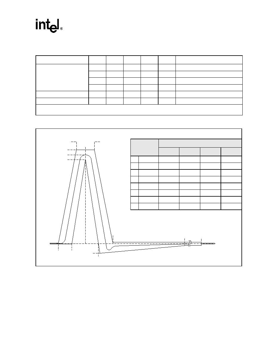
1168 Kbps HSDL Data Pump Chip Set -- SK70704/SK70707 or SK70708
Datasheet
45
Table 24. ACC Transmitter Electrical Parameters (Over Recommended Range)
Parameters
Sym
Min
Typ
Max
Unit
Test Conditions
Isolated pulse height at TTIP,
TRING
1
+2.455
+2.640
+2.825
Vp
TDATA High, TFP Low (+3)
-2.825
-2.640
-2.455
Vp
TDATA Low, TFP Low (-3)
+0.818
+0.880
+0.941
Vp
TDATA High, TFP High (+1)
-0.941
-0.880
-0.818
Vp
TDATA Low, TFP High (-1)
Setup time (TSGN, TMAG)
t
TSMSU
5
≠
≠
ns
Hold time (TSGN, TMAG)
t
TSMH
12
≠
≠
ns
1. Pulse amplitude measured across a 135
resistor on the line side of the transformer using the application circuit shown in
Figure 14
and
Table 18
.
Figure 17. ACC Normalized Pulse Amplitude Transmit Template
-1.2 T
-0.6 T
D = 0.93
B = 1.07
-0.4 T
0.4 T
C = 1.00
1.25 T
E = 0.03
14 T
G = -0.16
0.5 T
A = 0.01
F = -0.01
A = 0.01
F = -0.01
H = -0.05
50 T
T = 1.71
µ
s
Normalized
Levels
Quaternary Symbols (values in Volts)
+3
+1
-1
-3
A
.01
0.0264 0.0088
-0.0088
-0.0264
B
1.07
2.8248
0.9416
-0.9416
-2.8248
C
1.00
2.6400
0.8800
-0.8800
-2.6400
D
0.93
2.4552
0.8184
-0.8184
-2.4552
E
0.03
0.0792
0.0264
-0.0264
-0.0792
F
-0.01
-0.0264
-0.0088
0.0088
0.0264
G
-0.16
-0.4224
-0.1408
0.1408
0.4224
H
-0.05
-0.1320
-0.0440
0.0440
0.1320
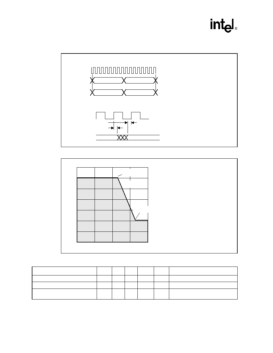
SK70704/SK70707 or SK70708 -- 1168 Kbps HSDL Data Pump Chip Set
46
Datasheet
Figure 18. ACC Transmitter Timing
Figure 19. Upper Bound of Transmit Power Spectral Density
Table 25. ACC Receiver Electrical Parameters (Over Recommended Range)
Parameter
Sym
Min
Typ
Max
Unit
Test Conditions
Propagation delay (AD0, AD1)
t
ADD
≠
≠
25
ns
Total harmonic distortion
≠
-80
≠
dB
V(RTIP, RRING) = 3 Vpp @ 50 kHz
RTIP, RRING, to BTIP, BRING gain
ratio
≠
1.0
1%
V/V
A) Transmit Syntax.
B) Transmit Timing.
t
TSMSU
t
TSMH
TCK4M
TSGN,
TMAG
TMAG
TSGN
TCK4M
-20
-40
-60
-80
-100
-120
-140
-160
1kHz
10kHz
100kHz
1MHz
10MHz
- 119 dBm/Hz
@ 2.92 MHz
Slope =
-80 dB/Decade
-39 dBm/Hz
@ 292 kHz
dB
m/Hz

1168 Kbps HSDL Data Pump Chip Set -- SK70704/SK70707 or SK70708
Datasheet
47
Figure 20. ACC Receiver Syntax and Timing
Table 26. HDX Absolute Maximum Ratings
Parameter
Symbol
Min
Max
Unit
Supply voltage
1
reference to ground
2
VCC2, VCC1
-0.3
+6.0
V
Input voltage
2
, any input pin
≠
- 0.3
VCC2 + 0.3
V
Continuous output current, any output pin
≠
≠
±25
mA
Storage temperature
T
STOR
-65
+150
∞C
Caution:
Operations at the limits shown may result in permanent damage to the HDSL Digital Transceiver
(HDX).
Normal operation at these limits is neither implied nor guaranteed
1. The maximum potential between VCC2 and VCC1 must never exceed ±1.2 V.
2. GND4 = GND3 = 0V; GND2 = 0V; GND1 = 0V.
Table 27. HDX Recommended Operating Conditions
Parameter
Symbol
Min
Typ
Max
Unit
DC supply
VCC1
1
3.95
5.0
5.25
V
VCC2
4.75
5.0
+5.25
V
VCC2-VCC1
-0.25
≠
+0.9
V
Ambient operating temperature
T
A
-40
≠
+85
∞C
1. To derive this supply, a 1N4001 (or equivalent) diode may be connected between VCC2 and VCC1 as shown in
Figure 14
and
Figure 15
. The diode should be selected to meet VCC1 minimum specifications.
B) Receive Timing
A) Receive Syntax
AGCKIK
AD1
AD0
FS
CK18M
INTERNAL)
CK37M
AD0,
AD1
AGCKIK
CLK37M
PROP DELAY
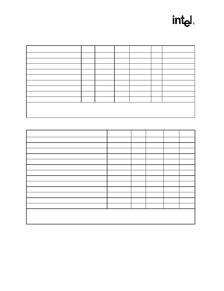
SK70704/SK70707 or SK70708 -- 1168 Kbps HSDL Data Pump Chip Set
48
Datasheet
Table 28. HDX DC Electrical Characteristics (Over Recommended Range)
Parameter
Sym
Min
Typ
1
Max
Unit
Test Conditions
Supply current (full operation)
Icc
≠
125
175
mA
Input Low voltage
V
IL
≠
≠
0.5
V
Input High voltage
V
IH
4.0
≠
≠
V
Output Low voltage
V
OL
≠
≠
GND +0.3
V
IOL < 1.6 mA
Output High voltage
V
OH
VCC2 - 0.5
≠
≠
V
I
OH
< 40
µ
A
Input leakage current
2
I
IL
≠
≠
±50
µ
A
0 < V
IN
< V
CC
2
Tristate leakage current
3
I
TOL
≠
≠
±30
µ
A
0 < V < V
CC
2
Input capacitance (individual pins)
C
IN
≠
12
≠
pF
Load capacitance (REFCLK output)
C
LREF
≠
≠
15
pF
1. Typical values are at 25 ∞C and are for design aid only; not guaranteed and not subject to production testing.
2. Applies to all pins that can be configured as inputs. Refer to
Table 2
for a complete list of signals.
3. Applies to SK70707 pins 8, 9, 14, 19, 21, 49, 51, 55, and 61-67 or SK70708 pins 7, 8, 10, 15, 17, 30, 32, and 36-43 when
tristated.
Table 29. HDX/HDSL Data Interface Timing (Figure 21)
Parameter
Symbol
Min
Typ
1
Max
Unit
ICLK frequency
f
ICLK
≠
1168
≠
kHz
REFCLK frequency
f
REFCLK
≠
18.688
≠
MHz
REFCLK frequency tolerance (LTU Mode)
tol
RCLK
-32
0
+32
ppm
CK9M frequency tolerance (NTU Mode)
2
tol
CK
6M
-32
0
+32
ppm
ICLK pulse width high
t
IPW
≠
428
≠
ns
Transition time on any digital output
3
t
TO
≠
5
10
ns
Transition time on any digital input
t
TI
≠
≠
25
ns
TDATA, TFP setup time to ICLK rising edge
t
TSU
100
≠
≠
ns
TDATA, TFP hold time from ICLK rising edge
t
TH
100
≠
≠
ns
RDATA, RFP, RFST delay from ICLK falling edge
t
TD
0
≠
150
ns
TFP pulse width
4
t
TFPW
828
856
884
ns
TFP falling edge to ICLK rising edge
4
t
TFIR
300
≠
400
ns
TFP setup time to REFCLK rising edge
4
t
TSUR
25
≠
≠
ns
1. Typical values are at 25 ∞C and are for design aid only; not guaranteed and not subject to production testing.
2. CK9M must meet this tolerance about an absolute frequency of 9.344000 MHz or 18.688000 MHz in NTU mode.
3. Measured with 15 pF load.
4. These parameters apply only to an LTU mode Data Pump programmed for repeater applications as shown in
Figure 21
.
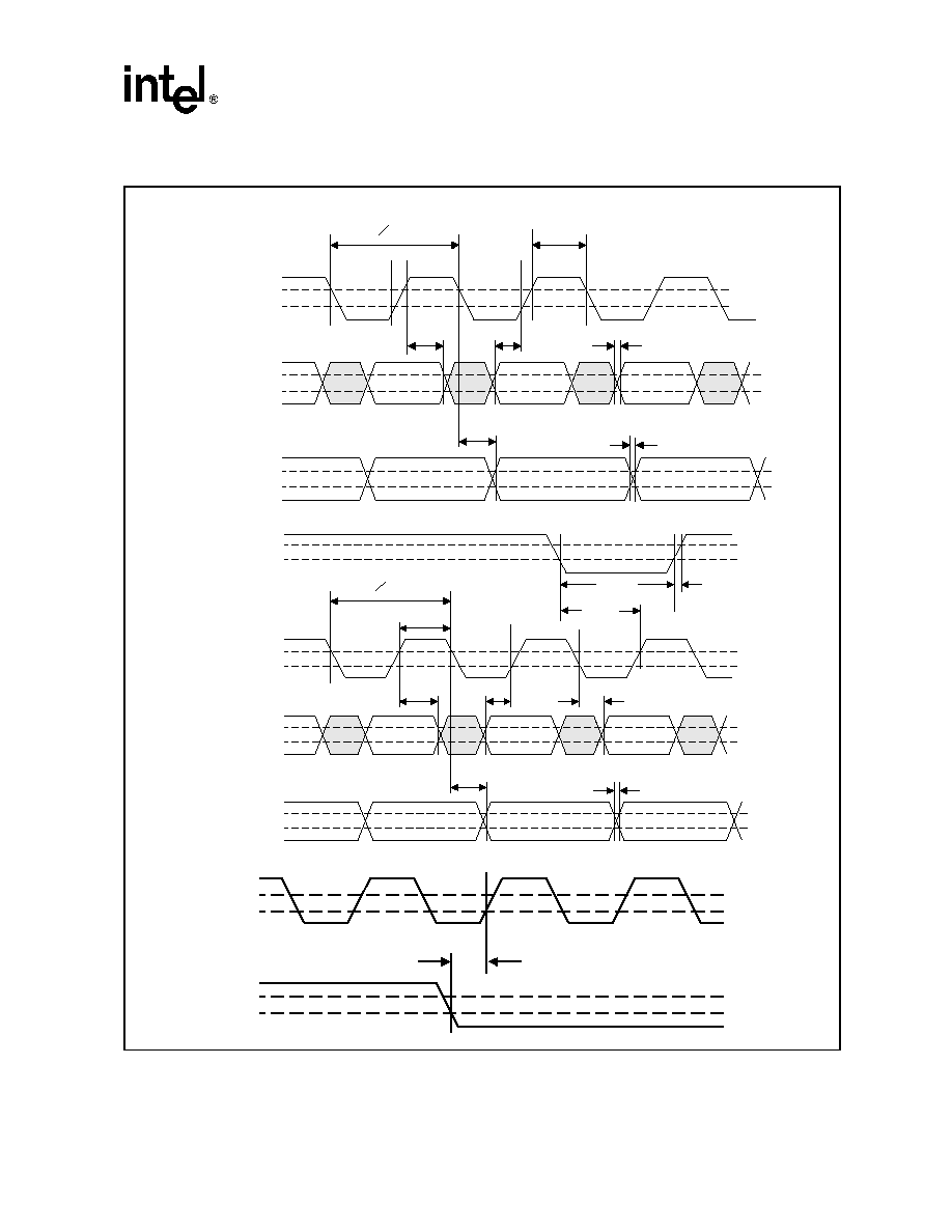
1168 Kbps HSDL Data Pump Chip Set -- SK70704/SK70707 or SK70708
Datasheet
49
Figure 21. HDX/HDSL Data Interface Timing
B) Repeater Mode
t
IPW
t
TH
t
TSU
t
TI
t
TD
t
TO
V
IL
V
IH
V
OH
V
OL
V
OH
V
OL
RATA,
RFP, RFST
TDATA,
TFP
ICLK
1
f
ICLK
t
IPW
t
TH
t
TSU
t
TD
t
TO
V
IL
V
IH
V
OH
V
OL
V
OH
V
OL
RATA,
RFP, RFST
TDATA
ICLK
t
TH
t
TI
t
TFIR
V
IL
V
IH
TFP
t
TFPW
1
f
ICLK
A) Non-Repeater Mode
REFCLK
TFP
t
TSUR
V
IH
V
IL
V
IH
V
IL
C) Repeater Mode
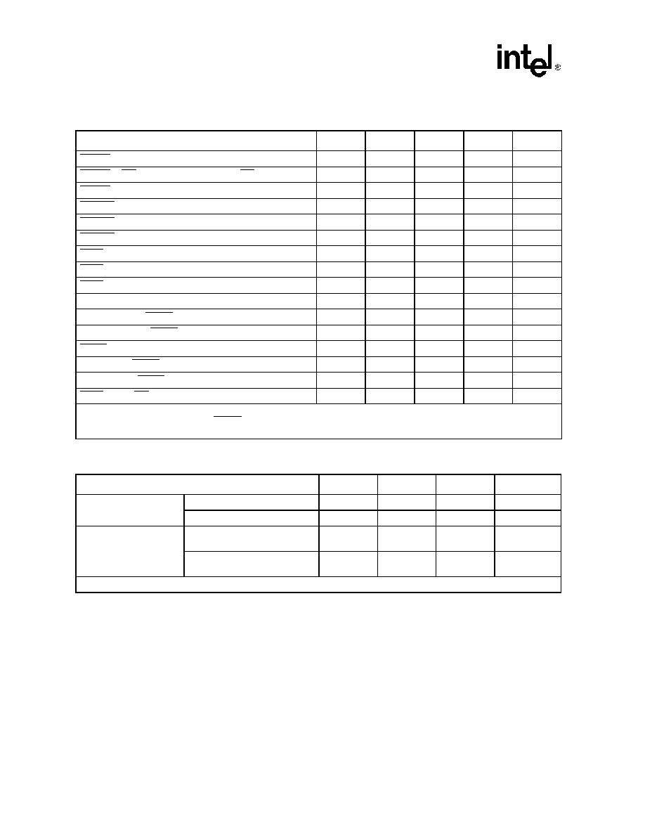
SK70704/SK70707 or SK70708 -- 1168 Kbps HSDL Data Pump Chip Set
50
Datasheet
Table 30. HDX/Microprocessor Interface Timing Specifications
1
(Figure 22 and Figure 23)
Parameter
Symbol
Min
Typ
Max
Unit
RESET2
pulse width Low
t
RPWL
0.1
≠
1,000
µ
s
RESET2
to
INT
clear (10 k
resistor from
INT
to VCC2)
t
INTH
≠
≠
300
ns
RESET2
to data tristate on D0-7
t
DTHZ
≠
≠
100
ns
CHIPSEL
pulse width Low
t
CSPWL
200
≠
≠
ns
CHIPSEL
Low to data active on D0-7
t
CDLZ
≠
≠
80
ns
CHIPSEL
High to data tristate on D0-7
t
CDHZ
≠
≠
80
ns
READ
pulse width Low
t
RSPWL
100
≠
≠
ns
READ
Low to data active
t
RDLZ
≠
≠
80
ns
READ
High to data tristate
t
RDHZ
≠
≠
80
ns
Address to valid data
2
t
PRD
≠
≠
80
ns
Address setup to
WRITE
rising edge
2
t
ASUW
20
≠
≠
ns
Address hold from
WRITE
rising edge
2
t
AHW
10
≠
≠
ns
WRITE
pulse width Low
t
WPWL
100
≠
≠
ns
Data setup to
WRITE
rising edge
t
DSUW
20
≠
≠
ns
Data hold from
WRITE
rising edge
t
DHW
10
≠
≠
ns
READ
High to
INT
clear when reading register RD0
t
INTR
≠
≠
400
ns
1. Timing for all outputs assumes a maximum load of 30 pF.
2. "Address" refers to input signals
CHIPSEL
, A0, A1, A2, and A3. "Data" refers to I/O signals D0, D1, D2, D3, D4, D5, D6, and
D7.
Table 31. General System and Hardware Mode Timing
Parameter
Min
Typ
1
Max
Unit
Throughput delay
TDATA to TTIP/TRING
≠
6.85
12.5
µ
s
RTINP/RRING to RDATA
≠
36.0
72
µ
s
Hardware mode
"ACTREQ" input transitional
pulse width (High or Low)
5
≠
≠
µ
s
"QUIET" transitional pulse width
(High-to-Low)
5
≠
≠
µ
s
1. Typical values are at 25∞ C and are for design aid only; not guaranteed and not subject to production testing.

1168 Kbps HSDL Data Pump Chip Set -- SK70704/SK70707 or SK70708
Datasheet
51
Figure 22.
Reset and Interrupt Timing
(
µ
P Control Mode)
A) Reset Timing
B) Interrupt Timing
t
RPWL
t
INTH
t
DTHZ
RESET2
INT
D0-7
(Output)
V
IH
V
IL
V
OH
V
OL
V
OL
V
OH
READ
V
IH
V
IL
CHIPSEL
t
INTR
ADDR0 - 3
INT
V
IH
V
IL
V
IH
V
IL
V
OH
V
OL
SK70704/SK70707 or SK70708 -- 1168 Kbps HSDL Data Pump Chip Set
52
Datasheet
Figure 23. Parallel Data Channel Timing
A) Chip Select Timing
B) Data Read Timing
C) Data Write Timing
V
IH
V
IL
CHIPSEL
V
OH
V
OL
t
RDLZ
t
PRD
READ
D0-7
(Output)
V
IH
V
IL
(WRITE = 1)
ADDR0-3
t
RDHZ
t
RSPWL
t
WPWL
V
IH
V
IL
CHIPSEL
V
IH
V
IL
t
DHW
WRITE
D0-7
(Input)
V
IH
V
IL
t
AHW
t
ASUW
(READ = 1)
ADDR0-3
t
TI
t
DSUW
V
IH
V
IL
CHIPSEL
t
CSPWL
V
OH
V
OL
t
CDLZ
t
CDHZ
(READ = 0)
D0-7
(Output)
1168 Kbps HSDL Data Pump Chip Set -- SK70704/SK70707 or SK70708
Datasheet
53
5.0
Mechanical Specifications
Figure 24. ACC Plastic Leaded Chip Carrier Package Specifications
Analog Core Chip (ACC)
∑
28-pin PLCC
∑
P/N SK70704PE (-40∞ to + 85∞ C)
Dim
Inches
Millimeters
Min
Max
Min
Max
A
0.165
0.180
4.191
4.572
A1
0.090
0.120
2.286
3.048
A2
0.062
0.083
1.575
2.108
B
.050
BSC
1
(nominal)
1.27
BSC
1
(nominal)
C
0.026
0.032
0.660
0.813
D
0.485
0.495
12.319
12.573
D1
0.450
0.456
11.430
11.582
F
0.013
0.021
0.330
0.533
1. BSC--Basic Spacing between Centers
D
1
D
C
B
CL
D
F
A
2
A
1
A
SK70704/SK70707 or SK70708 -- 1168 Kbps HSDL Data Pump Chip Set
54
Datasheet
Figure 25. HDX Plastic Leaded Chip Carrier Package Specifications
A
2
A
D
F
A
1
C
B
D
1
D
CL
SK70707 HDSL Digital Transceiver (HDX)
∑
68-pin PLCC
∑
P/N SK70707PE (-40∞ to + 85∞ C)
Dim
Inches
Millimeters
Min
Max
Min
Max
A
0.165
0.180
4.191
4.572
A1
0.090
0.120
2.286
3.048
A2
0.062
0.083
1.575
2.108
B
.050
BSC
1
(nominal)
1.27
BSC
1
(nominal)
C
0.026
0.032
0.660
0.813
D
0.985
0.995
25.019
25.273
D1
0.950
0.958
24.130
24.333
F
0.013
0.021
0.330
0.533
1. BSC--Basic Spacing between Centers
A
2
D
F
A
1
D
1
D
CL
C
B
A
SK70708 HDSL Digital Transceiver (HDX)
∑
44-pin PLCC
∑
P/N SK70708PE (-40∞ to + 85∞ C)
Dim
Inches
Millimeters
Min
Max
Min
Max
A
0.165
0.180
4.191
4.572
A1
0.090
0.120
2.286
3.048
A2
0.062
0.083
1.575
2.108
B
.050
BSC
1
(nominal)
1.27
BSC
1
(nominal)
C
0.026
0.032
0.660
0.813
D
0.685
0.695
17.399
17.653
D1
0.650
0.656
16.510
16.662
F
0.013
0.021
0.330
0.533
1. BSC--Basic Spacing between Centers