Document Outline
- FEATURES
- FUNCTIONAL DESCRIPTION
- BLOCK DIAGRAM
- PIN CONFIGURATION
- ENCODER OPERATION
- DECODER OPERATION
- INPUT SIGNALS
- OUTPUT SIGNALS
- ELECTRICAL CHARACTERISTICS
- ABSOLUTE MAXIMUM RATINGS
- RECOMMENDED OPERATING CONDITIONS
- D C CHARACTERSITICS
- ENCODER TIMING
- DECODER TIMING (a) PARRALLEL INPUT MODE (PARL=1)
- DECODER TIMING (b) PARRALLEL INPUT MODE (PARL=0)
- DECODER A C CHARACTERISTICS
- NODE SYNCHRONIZATION
- PUNCTURED CODE OPERATION
- APPLICATIONS INFORMATION
- APPLICATION INFORMATION

R
STEL-2030C
17 Mbps
Convolutional Encoder
Viterbi Decoder
STEL-2030C
Data Sheet

STEL-2030C
2
FUNCTIONAL DESCRIPTION
Convolutional Encoding and Viterbi Decoding are used to
provide forward error correction (FEC) which improves
digital communication performance over a noisy link. In
satellite communication systems where transmitter power is
limited, FEC techniques can reduce the required transmission
power. The STEL-2030C is a specialized product designed
to perform this specific communications related function. It
is functionally identical to the previously available STEL-
2030B, which it replaces.
The encoder creates a stream of symbols which are
transmitted at twice the information rate. This encoding
introduces a high degree of redundancy which enables
accurate decoding of the information despite a high symbol
error rate resulting from a noisy communications link.
FEATURES
n 17 Mbps MAX. OPERATING DATA RATE
n CONSTRAINT LENGTH K = 7
G
1
= 171
8
, G
2
= 133
8
n MULTIPLE DEVICES CAN BE
MULTIPLEXED TO GIVE HIGHER DATA
RATES
n OPTIMIZED INTERFACE TO OPERATE
WITH BPSK, QPSK, AND OQPSK
DEMODULATORS
n V.35 SCRAMBLER AND DESCRAMBLER
WITH CCITT AND IESS OPTIONS
n DIFFERENTIAL ENCODER AND
DECODER
n AUTO NODE SYNC CAPABILITY
n INTERNAL BER MONITOR
n MULTIPLE RATES:
R =
1
/
2
,
2
/
3
*,
3
/
4
* (* Punctured codes)
n INTERNAL PUNCTURING CAPABILITY
n 5.2 dB CODING GAIN @10
-5
BER
n 84-PIN PLCC PACKAGE
BLOCK DIAGRAM
EG2 (133
8
)
EG1 (171
8
)
7-BIT SHIFT REGISTER
Q1
Q2
Q3
Q4
Q5
Q6
Q7
EDAT
ECLKIN
ESCRAM
EDIF
ERESET
V.35
SCRAMBLER
ECLKOUT
ESEL
SYMBOL
ALIGNMENT
CIRCUIT
METRIC
ASSIGNMENT
VITERBI
DECODER
(ACS)
TRACEBACK
MEMORY
TIMING AND
CONTROL
G1
2-0
G2
2-0
PNCG1/G2
DCLKIN
DIFFERENTIAL
DECODER
DATO
AUTO
SYNC
BER
MONITOR
BERR
CLKSEL
V.35
DESCRAMBLER
G1ERR
G2ERR
OOS
ODCLK
DDIF
DSCRAM
DRESET
LDG2
PARL
OQPSK
OBIN
COUNT
THR
DSEL
8
8
2
3
3
TBD

3
STEL-2030C
Notes: I.C. denotes Internal Connection. These pins must be left unconnected. Do not use for vias.
N.C. denotes No Connection. These pins can be used for vias.
PIN CONNECTIONS
1 V
DD
2 V
SS
3 THR
0
4 THR
1
5 THR
2
6 THR
3
7 THR
4
8 V
SS
9 THR
5
10 THR
6
11 THR
7
12 ECLKIN
13 EDIF
14 ESCRAM
15 ESEL
16 V
SS
17 ERESET
18 EDAT
19 V
DD
20 DRESET
21 DCLKIN
22 V
SS
23 PNCG2
24 G2
0
25 G2
1
26 G2
2
27 PNCG1
28 V
SS
29 G1
0
30 G1
1
31 G1
2
32 LDG2
33 SYNC
34 OBIN
35 PARL
36 OQPSK
37 V
SS
38 DSCRAM
39 DSEL
40 DDIF
41 TBD
42 V
SS
43 N.C.
44 V
DD
45 CLKSEL
46 V
DD
47 V
DD
48 N.C.
49 N.C.
50 V
DD
51 V
SS
52 N.C.
53 V
SS
54 I.C.
55 N.C.
56 N.C.
57 V
SS
58 V
DD
59 OOS
60 AUTO
61 N.C.
62 N.C.
63 V
SS
64 BERR
65 V
DD
66 G2ERR
67 G1ERR
68 ODCLK
69 DATO
70 V
DD
71 V
SS
72 EG2
73 EG1
74 ECLKOUT
75 V
SS
76 COUNT
0
77 COUNT
1
78 COUNT
2
79 COUNT
3
80 V
SS
81 COUNT
4
82 COUNT
5
83 COUNT
6
84 COUNT
7
PIN CONFIGURATION
The STEL-2030C contains a K = 7 convolutional encoder
and Viterbi decoder (including differential, as well as direct
encoding/decoding) capable of fully independent (full
duplex) operation, with completely independent data clocks.
At the decoder the symbol input format can be either serial,
i.e., sequential symbols, (typically for BPSK applications)
or parallel (typically for QPSK and OQPSK applications).
The data inputs can be in offset binary or offset signed
magnitude formats, with 3-bit soft decision. Auto node sync
and a BER monitor are also provided in the device. Rate
2
/
3
and
3
/
4
punctured signals can be encoded and decoded, as
well as non-punctured, Rate
1
/
2
, signals. The polynomials
used are industry standards.
Package: 84-pin PLCC
Thermal coefficient, q
ja
= 30∞ C/W
Notes: (1) Tolerances on pin spacing are not cumulative
(2) Dimensions at seating plane
0.200"
max.
1.190"
± 0.005"
3 3 3 3 3 3 3 4 4 4 4 4 4 4 4 4 4 5 5 5 5
3 4 5 6 7 8 9 0 1 2 3 4 5 6 7 8 9 0 1 2 3
1 1
8 8 8 8 8 7 7 7 7 7
1 0 9 8 7 6 5 4 3 2 1 4 3 2 1 0 9 8 7 6 5
12
13
14
15
16
17
18
19
20
21
22
23
24
25
26
27
28
29
30
31
32
74
73
72
71
70
69
68
67
66
65
64
63
62
61
60
59
58
57
56
55
54
0.017"
± 0.004" (2)
1.154"
± 0.004"
0.05"
nominal (1)
Top View

STEL-2030C
4
ENCODER OPERATION
The convolutional coder is functionally independent from
the decoder. A single data bit is clocked into the 7-bit shift
register on the rising edge of ECLKIN. Two symbols, G1
and G2, are generated and are brought out on separate pins,
EG1 and EG2.
DECODER OPERATION
The decoder section of the STEL-2030C implements the
Viterbi algorithm for decoding convolutionally encoded
data. It incorporates many unique features which enhance
its capabilities and flexibility. The incoming symbols can
be accepted either sequentially, as would be the case in a
BPSK system, or in parallel, as would be the case in a QPSK
system. In addition, a special circuit takes care of symbol
alignment in an Offset QPSK (OQPSK) system. The signals
can be in either offset binary or signed magnitude codes. In
both cases the codes are offset from zero by half a quantization
level, giving the same number of allowable states in both the
positive and negative directions.
The Viterbi decoder itself uses the add/compare/select
algorithm to determine the most likely value for each bit
from the trellis created from the received symbols. Five-bit
arithmetic is used to maximize the performance with the
three-bit soft-decision data inputs. The decoder contains
many user controlled features which enhance its performance
in different environments. The depth of the trace-back used
can be set to the long mode (70 states) for optimum
performance in the punctured modes (R =
2
/
3
,
3
/
4
,
7
/
8
), or to
the short mode (38 states) in normal mode (R =
1
/
2
). (The
penalty for using the longer trace-back length is the additional
delay in decoding the data.) A built-in counter estimates the
probability of incorrect node synchronization from the error
rate. A user selectable feedback loop allows the node
synchronization to be corrected automatically, and the device
also features a built-in bit error-rate (BER) monitor circuit
as well as a V.35 descrambler. The true CCITT V.35
algorithm is supported as well as the IESS version of this
algorithm.
INPUT SIGNALS
ERESET
Encoder Reset. A logic low on this asynchronous input will
completely reset all internal registers in the encoder to an
initial condition within 100 nanoseconds. This sets the
encoder state to all zeroes.
ECLKIN
The transmit clock is the encoder system clock. The
maximum ECLKIN frequency is 17 MHz. There is no
minimum frequency. Data is latched into the encoder on the
falling edges of this clock.
EDAT
The encoder input data is connected to this input. The data
is clocked in on the falling edge of the ECLKIN signal.
EDIF
When the EDIF signal is set high it enables the differential
encoder circuit. When it is set low this circuit will be
disabled, and normal, non-differential data will be loaded
into the convolutional encoder.
ESCRAM
When this input is set high it causes the encoded data to be
scrambled before being differentially encoded and before
being convolutionally encoded. The scrambling algorithm
used is the standard CCITT or IESS V.35 algorithms
according to the setting of ESEL.. When ESCRAM is set
low the scrambler function will be inhibited.
ESEL
When this input is set low the CCITT compatible mode is
selected for the V.35 scrambler in the encoder, and when it
is set high the IESS compatible mode is selected.
DRESET
Decoder Reset. A logic low on this asynchronous input will
completely reset all registers in the decoder to an initial
condition within 3 clock cycles. This will not affect the
values stored in the decision path memory.
DCLKIN
Decoder clock input. It is the reference clock for all internal
synchronous functions in the decoder. It should nominally be
a square wave. When CLKSEL is set low the DCLKIN signal
should be at twice the frequency of the input symbols, with a
maximum frequency of 68 MHz when PARL = 0 and 34 MHz
when PARL = 1, corresponding to a decoded data rate of 17
Mbps. When CLKSEL is set high the DCLKIN signal should
be at the same frequency as the input symbols, with a maximum
frequency of 20 MHz when PARL = 0 and 10 MHz when
PARL = 1, corresponding to a decoded data rate of 10 Mbps.

5
STEL-2030C
G1
2-0
, G2
2-0
The G1
2-0
and G2
2-0
signals are the 3-bit soft decision input
symbols to the decoder. They are presented to the decoder
either sequentially or in parallel depending on the state of
the PARL signal. In the parallel mode (PARL = 1) the
symbols are clocked into the device on the falling edge of
DCLKIN (alternate edges only when CLKSEL = 0). In the
sequential mode (PARL = 0) the G2
2-0
inputs are not used,
both the G1 and G2 symbols are loaded via the G1
2-0
pins.
The G1 symbols are then latched in on the falling edges of
DCLKIN when LDG2 is low and the G2 symbols are
latched in on the falling edges of DCLKIN when LDG2 is
high.
OBIN
The STEL-2030C can accept the soft-decision input data in
either offset binary or signed magnitude formats. When the
OBIN signal is set high the format expected will be offset
binary, and when it is set low it will be signed magnitude.
The meanings of the 3-bit values for these two codes is
shown in the table.
OBIN = 1
OBIN = 0
Value
111
111
Most confident +
110
110
(Data = 1)
101
101
100
100
Least confident +
011
000
Least confident
010
001
001
010
(Data = 0)
000
011
Most confident
When using the STEL-2030C with hard-decision data the
symbols should be loaded into the G1
2
and G2
2
pins. The
other symbol inputs should be set to a logic high level and
OBIN should be set low.
LDG2
When this signal is high during a rising edge of DCLKIN
the symbol loaded into the G1
2-0
pins on the next falling
edge of DCLKIN will be G2. This function is only active
when PARL is set low (sequential input mode).
PARL
When this signal is high the input symbols are accepted in
parallel by the chip, using the G1
2-0
pins for the G1 symbols
and the G2
2-0
pins for the G2 symbols. When it is set low the
inputs are accepted sequentially, using the G1
2-0
pins for
both symbols. The sequential input is most suited for BPSK
data and the parallel input is most suited for QPSK data.
OQPSK
When this signal is high the device is set up to operate with
Offset QPSK (OQPSK) data. This is only valid when
PARL is also set high.
DDIF
When this input is set high it causes the data out of the
Viterbi decoder to be differentially decoded. This function
precedes the descrambler.
DSCRAM
When this input is set high it causes the data out of the
Viterbi decoder to be descrambled. The descrambling
algorithm used is the CCITT or IESS V.35 algorithms
according to the setting of DSEL, and descrambling follows
differential decoding when this is enabled. When the
DSCRAM signal is set low, this function will be inhibited.
DSEL
When this input is set low the CCITT compatible mode is
selected for the V.35 descrambler in the decoder is set into
and when it is set high the IESS compatible mode is selected.
PNCG1, PNCG2
The PNCG1 and PNCG2 signals are used to control the
STEL-2030C when operating in punctured mode. In normal
(Rate =
1
/
2
) operation these pins should be set low. In
punctured mode the PNCG1 signal must be set high to
indicate that the G1 symbol is punctured and the PNCG2
signal must be set high to indicate that the G2 symbol is
punctured. A symbol will be punctured when the PNCG1
or PNCG2 signals are high during the falling edge of
DCLKIN which latches the corresponding symbol in to the
decoder. Zero value metrics will be substituted internally
for the actual metrics corresponding to the signals present
on the G1
2-0
or G2
2-0
pins at that time.
TBD
This signal selects the Trace-Back Depth used in the decoding
process. When it is set low the traceback depth will be 70
states, and when it is set high the traceback depth will be 38
states. The longer traceback depth gives better performance,
especially in the punctured modes; the shorter traceback
depth gives a shorter latency.
SYNC
When the SYNC input is set high during the rising edge of
DCLKIN the internal symbol synchronization will be
changed. When auto node sync is not desired this pin should
be set low. It should be connected to the AUTO output to
use the auto node sync capability of the STEL-2030C. The
state of this circuit will always be set to normal after a reset.

STEL-2030C
6
COUNT
7-0
This 8-bit input signal defines the period (number of bits)
used in the node synchronization circuit. The 8-bit number
N is used to set up a period of (256N+256) internally, where
N is the value of COUNT
7-0
. If the renormalization count
exceeds the threshold value during a period of this number
of bits then an out-of-sync condition is declared (i.e., the
output pin OOS is switched to High and AUTO is toggled).
THR
7-0
This 8-bit input signal defines the threshold for node
synchronization. The 8-bit number N is used to set up a
threshold value of (8N+2) internally, where N is the value of
THR
7-0
. If the renormalization count is greater than this
threshold value then an out-of-sync condition is declared
(i.e., the output pin OOS is switched to High and AUTO is
toggled).
CLKSEL
When Clock Select is set low the STEL-2030C operates in
its normal mode with DCLKIN running at twice the input
symbol rate. When it is set high the device operates in the
alternative mode with DCLKIN running at the same rate as
the input symbols. This allows the device to be used in
circuits having this clock requirement.
OUTPUT SIGNALS
EG1, EG2
The EG1 and EG2 signals are the two encoded sym-bols
generated with the polynomials G1 = 171
8
and G2 = 133
8
.
ECLKOUT
This signal is a replica of the ECLKIN signal. The output
signals G1 and G2 change on the rising edges of this clock.
DATO
Decoded data output. This is the output of the Viterbi
decoder. The output data bits are delayed by 163 clock
cycles relative to the corresponding input symbols, G1
2-0
and G2
2-0
when operating in the short trace-back depth
mode (TBD = 1), and 291 clock cycles when operating in the
long trace-back depth mode (TBD = 0). This
signal changes on the rising edges of ODCLK.
ODCLK
Output data clock. All outputs change on the rising edge of
this clock. The falling edge of ODCLK can be used as a
strobe for DATO output, which is guaranteed to be valid on
this edge. Note that when CLKSEL = 0 and PARL = 1 the
frequency of ODCLK is twice that of the data. If this clock
is divided by 2 with a divider triggering on the falling edge
of the clock the data will always be valid on the rising edge
of the divider output.
OOS
This output pin serves as a flag for the out-of-sync condition.
When it goes high it signifies that the renormalization count
in the internal node sync circuit has exceeded the threshold
value set by the THR
7-0
signal and the out-of-sync condition
is declared. It will remain high until this condition ceases to
exist. i.e., the next time the threshold is not exceeded during
a complete count period.
AUTO
This is the feedback signal from the internal node sync
correction circuit. It will pulse high for one cycle of
DCLKIN each time the renormalization count in the internal
node sync circuit has exceeded the threshold value set by the
THR
7-0
signal and the out-of-sync condition is declared. It
should be connected to the SYNC input when using the
internal node sync facility.
BERR
The Bit Error output indicates that an error has been
detected in either the G1 or G2 symbols corresponding to
the current output bit. Note that when operating with
punctured codes (Rates
2
/
3
and
3
/
4
) the BERR output will
pulse once for each symbol during which either PNCG1 or
PNCG2 is set high. There will be a delay corresponding to
the throughput delay of the decoder and encoder circuits
between each instance of PNCG2 or PNCG2 being set high
and the corresponding pulse on BERR.
G1ERR
The G1 Error output indicates that an error has been detected
in the G1 symbol corresponding to the current output bit. Note
that when operating with punctured codes (Rates
2
/
3
and
3
/
4
) the
G1ERR output will pulse once for each symbol during which
PNCG1 is set high. There will be a delay corresponding to the
throughput delay of the decoder and encoder circuits between
each instance of PNCG1 being set high and the corresponding
pulse on G1ERR.
G2ERR
The G2 Error output indicates that an error has been detected
in the G2 symbol corresponding to the current output bit. Note
that when operating with punctured codes (Rates
2
/
3
and
3
/
4
) the
G2ERR output will pulse once for each symbol during which
PNCG2 is set high. There will be a delay corresponding to the
throughput delay of the decoder and encoder circuits between
each instance of PNCG2 being set high and the corresponding
pulse on G2ERR.
7
STEL-2030C
ELECTRICAL CHARACTERISTICS
ABSOLUTE MAXIMUM RATINGS
Warning:
Stresses greater than those shown below may cause permanent damage to the
device. Exposure of the device to these conditions for extended periods may also affect device
reliability.
Symbol
Parameter
Range
Units
T
s
Storage Temperature
≠40 to +125 ∞C
(Plastic package)
≠55 to +125 ∞C
(Ceramic package)
T
a
Operating Temperature
≠40 to +85
∞C
(Plastic package)
≠55 to +125 ∞C
(Ceramic package)
V
DDmax
Max. voltage between V
DD
and V
SS
+7 to ≠0.7
volts
V
I/O(max)
Max. voltage on any input or output pin
V
DD
+ 0.3
volts
V
I/O(min)
Min. voltage on any input or output pin
V
SS
≠ 0.3
volts
RECOMMENDED OPERATING CONDITIONS
Symbol
Parameter
Range
Units
V
DD
Supply Voltage
+5 ± 5%
volts
T
a
Operating Temperature (Ambient)
0 to +70
∞C (Plastic package)
≠55 to +125 ∞C (Ceramic package)
D.C. CHARACTERISTICS
(Operating Conditions: V
DD
= 5.0 ± 5% volts, T
a
= 0∞ to 70∞ C)
Symbol
Parameter
Min.
Typ.
Max.
Units
Conditions
I
DD(Q)
Supply Current, Quiescent
1.0
mA
Static, no clock
I
DD
Supply Current, Operational
2
mA/Mbps
CLKSEL
= 0, PARL = 0
I
DD
Supply Current, Operational
8
mA/Mbps
All other modes
V
IH(min)
Min. High Level Input Voltage
2.0
volts
Guaranteed Logic '1'
V
IL(max)
Max. Low Level Input Voltage
0.8
volts
Guaranteed Logic '0'
V
OH(min)
Min. High Level Output Voltage
2.4
volts
I
O
= ≠4.0 mA
V
OL(max)
Max. Low Level Output Voltage
0.4
volts
I
O
= +4.0 mA
I
IH(max)
Max. High Level Input Current
10
µA
V
IN
= +5.0 volts
I
IL(max)
Max. Low Level Input Current
≠10
µA
V
IN
= 0 volts
{
{
{
STEL-2030C
8
ENCODER A.C. CHARACTERISTICS
(Operating Conditions: V
DD
= 5.0 ± 5% volts, T
a
= 0∞ to 70∞ C)
Symbol
Parameter
Min.
Max.
Units
Conditions
t
DS
EDAT
to ECLKIN setup
10
nsec.
t
DH
EDAT
to ECLKIN hold
5
nsec.
t
ECC
ECLKIN
to ECLKOUT stable delay
30
nsec.
t
ECD
ECLKOUT
to G1 G2 stable delay
5
nsec.
f
ECLK
ECLKIN
frequency
17
MHz
DECODER A.C. CHARACTERISTICS
(Operating Conditions: V
DD
= 5.0 ±5% volts, T
a
= 0∞ to 70∞ C)
Symbol
Parameter
Min.
Max.
Units
Conditions
f
DAT
Data speed
17
Mbps
t
SU
G1
, G2, PNCG1 or PCNG2 to DCLKIN Setup
10
nsecs.
t
HD
G1
, G2, PNCG1 or PCNG2 to DCLKIN Hold
5
nsecs.
t
CD
DCLKIN
to ODCLK stable delay
20
nsecs.
t
OD
ODCLK
to any other output stable delay
12
nsecs.
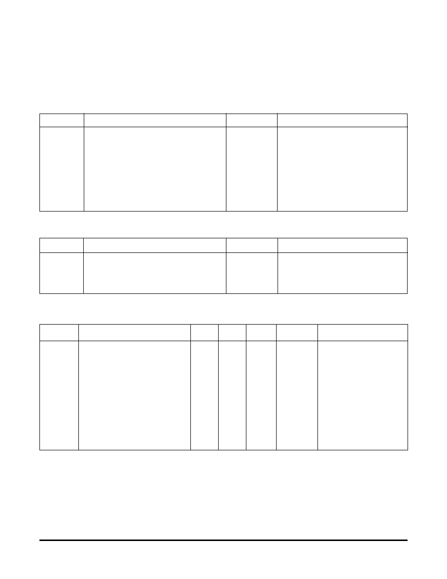
ENCODER TIMING
E C L K O U T
E G 1 , E G 2
E D AT
B I T 1
B I T 2
BIT 3
B IT 4
X
X
X
X
E C L K IN
t
D S
t
D H
t
EC D
t
EC C
9
STEL-2030C
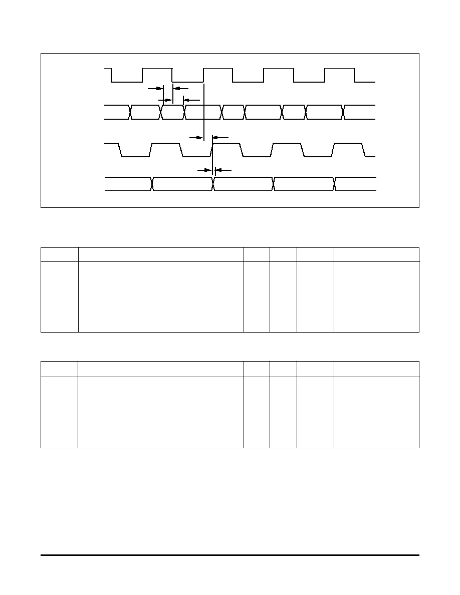
DECODER TIMING (a) PARALLEL INPUT MODE (PARL = 1)
1. CLKSEL = 1
2. CLKSEL = 0
G1/G2
DCLKIN
DATO
BIT 2
BIT 1
PNCG1/G2
SYMB. N
SYMB. N+1
SYMB. N+2
BIT 0
BIT 2
BIT 3
BIT 4
SYMB. N+3
SYMB. N+4
SYMB. N+5
ODCLK
SYMB. N-1
t
SU
t
HD
t
OD
t
CD
DATO
BIT 2
BIT 1
SYMB. N-1
SYMB. N
SYMB. N+1
SYMB. N+2
BIT 0
BIT 2
BIT 3
BIT 4
SYMB. N+3
SYMB. N+4
SYMB. N+5
DCLKIN
G1/G2
PNCG1/G2
ODCLK
t
SU
t
HD
t
OD
t
CD
Notes: 1. N = 163 when TBD = 1, N = 291 when TBD = 0
2. When CLKSEL = 1 an internal double speed clock is generated whose
rising edges are generated on the edges of DCLKIN.

STEL-2030C
10
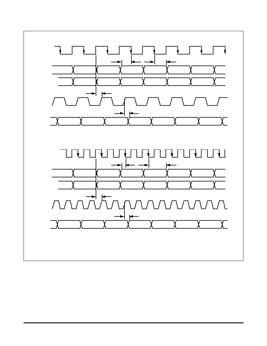
DECODER TIMING (b) SEQUENTIAL INPUT MODE (PARL = 0)
1. CLKSEL = 1
2. CLKSEL = 0
Note: When CLKSEL = 1 an internal double speed clock is generated whose
rising edges are generated on the edges of DCLKIN.
G1/2
G1
G2
G2
DATO
LDG2
DCLKIN
PNCG1/G2
G1
G2
G1
G2
G1
ODCLK
t
SU
t
HD
t
OD
t
CD
t
SU
t
HD
G1/2
G1
G2
G2
DATO
LDG2
DCLKIN
PNCG1/G2
G1
G2
G1
G2
G1
ODCLK
t
SU
t
HD
t
OD
t
CD
t
SU
t
HD

11
STEL-2030C
DECODER A.C. CHARACTERISTICS
(Operating Conditions: V
DD
= 5.0 ±5% volts, T
a
= 0∞ to 70∞ C)
Symbol
Parameter
Min.
Max.
Units
Conditions
f
DAT
Data speed
17
Mbps
t
SU
G1
, G2, PNCG1 or PCNG2 to DCLKIN Setup
10
nsecs.
t
HD
G1
, G2, PNCG1 or PCNG2 to DCLKIN Hold
5
nsecs.
t
CD
DCLKIN
to ODCLK stable delay
20
nsecs.
t
OD
ODCLK
to any other output stable delay
12
nsecs.
NODE SYNCHRONIZATION
In a communication system using Viterbi decoding the
decoder will only operate correctly when the symbols G1
and G2 are loaded into the decoder in the correct order.
Identifying which symbol is which is referred to as node
synchronization. The STEL-2030C contains a circuit
designed to carry out the node synchronization function
automatically. It uses the internally generated metrics of the
received sequence to do this. These parameters are constantly
changing and are periodically renormalized to keep them
within bounds. If renormalization is required too frequently
it is a good indication that the system is not converging, and
the most likely reason is lack of node synchronization. The
renormalization rate at which the system will decide to
change the node sync is determined by the threshold
parameter. This is an 8-bit number which is set by the
THR
7-0
inputs. When the renormalization count exceeds
this value, the OOS output will go high and the AUTO
output will pulse high for one clock cycle. The counter is
reset after a number of bits determined by the number set by
the COUNT
7-0
inputs, so that the threshold must be exceeded
somewhere in that period for resynchronization to take
place. To use the internal node sync the AUTO output must
be connected to the SYNC input. The synchronization
sequence depends on the setting of the PARL input. When
PARL is set low it is assumed that the data was modulated
using BPSK, and when it is set high it is assumed that the
data was modulated using QPSK, the appropriate
synchronization sequences will be invoked, as shown in the
table:
Symbol entered into
decoder during
symbol period N
PARL Sync State
G1
2-0
G2
2-0
0
0
G1
N
G2
N
0
1
G2
N1
G1
N
1
0
G1
N
G2
N
1
1
G2
N
G1
N
Sync state 0 is the state into which the device will be set after
a reset sequence. Note that whenever the sync state is
changed there will be a delay of 163 or 291 bit periods
before valid data starts appearing at DOUT, according to
the state of the TBD input.
The most suitable threshold setting will depend on both the
value of E
b
/N
0
and the signal level at the G1 and G2 inputs.
For full scale inputs, i.e., the peak signal values almost
saturate the digital inputs, a suitable starting value for the
threshold will be 10%. e.g. if the number of bits over which
the measure is made is set to 256 (COUNT
7-0
= 0) the
threshold should be set to 26 (THR
7-0
= 3). More reliable
results will be obtained by counting over a longer period to
improve the averaging process, but this increases the time
taken to make a decision and hence to acquire node sync.
Thus starting with a low count period and then increasing it (and
adjusting the threshold accordingly to maintain a value of 10%)
will result in a faster acquisition of correct node sync followed
by a better chance of recorrecting if an error was made.
STEL-2030C
12
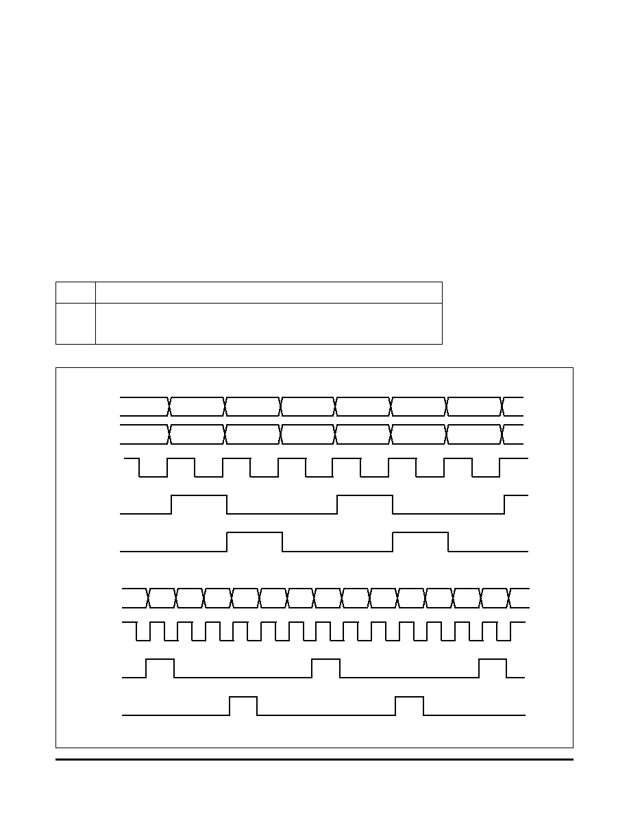
G1/2
DCLKIN
G2
G1
G2
G1
G2
G1
G2
G1
G2
G1
G2
G1
G2
G1
G2
PNCG1
PNCG2
*
*
*
*
*
G1
DCLKIN
G2
PNCG1
PNCG2
*
*
*
*
*
(a) PARALLEL INPUT MODE (PARL = 1)
(b) SEQUENTIAL INPUT MODE (PARL = 0)
Rate
Symbol sequence
2
/
3
G1 G2 G1 P
G1 G2 G1 P G1 G2 G1 P G1 G2 G1 P G1 G2
3
/
4
G1 G2 P G2 G1 P
G1 G2 P G2 G1 P G1 G2 P G2 G1 G2
zero metric values. Zero weight is given to these values in
the computations relative to the other symbols. The coding
gain is significantly less than that for unpunctured operation,
as shown in the BER plot, but this is the trade-off for the
reduced bandwidth required to transmit the symbols. The
puncturing sequences for the various
(N-1)
/
N
rates of punctured
operation are shown in the table. The sequence shown in
boldface is the basic sequence, which is then repeated. The
use of the PNCG1 and PNCG2 signals is shown below for
Rate
3
/
4
. The sequence is G1 G2 P G2 G1 P. The punctured
symbols are marked with asterisks. Rates higher than
3
/
4
are
not recommended with the STEL-2030C.
In punctured codes some of the symbols generated by the
convolutional encoder are deleted, or punctured, from the
transmitted sequence. For example, in an unpunctured Rate
1
/
2
sequence, four bits would be transmitted for every two
data bits. I f every fourth bit was punctured from the
sequence then only three bits would be transmitted for every
two data bits. This would result in a Rate
2
/
3
code. The
STEL-2030C decoder is designed to operate in punctured
mode as well as normal, Rate
1
/
2
, mode. This is easily
accomplished by means of the PNCG1 and PNCG2 signals,
which delete the symbol which would normally have been
loaded into the device at the time when either of these
signals is set high. The punctured symbols are replaced by
PUNCTURED CODE OPERATION
Note: Timing shown for case where CLKSEL = 1. DCLKIN runs at double the speed when CLKSEL = 0.

13
STEL-2030C
BER PERFORMANCE WITH RATE
1
/
2
AND PUNCTURED CODES
BER
E
b
/N
0
(dB)
1
2
3
4
5
6
10
-7
10
-6
10
-5
10
-4
10
-3
10
-2
10
-1
rate=1/2theory
rate=1/2
rate=2/3
rate=3/4
APPLICATIONS INFORMATION
BPSK OPERATION OF ENCODER
The STEL-2030C encoder generates output symbols as
parallel pairs, suitable for QPSK modulation. For BPSK
modulation it is normally necessary to serialize the symbol
pairs using a clock at twice the data rate. A suitable
circuit is shown below in which the input clock is divided
by two to produce the data clock itself. The encoder
produces parallel symbol pairs and the multiplexer
serializes them for BPSK modulation.
D Q
Q
ECLKIN
EDAT
EG1
A2
QA
STEL-2030C
BPSK Out
Data
Clock
2X Data
Clock
Data In
74AC74 (
1
/
2
)
EG2
WS
A1
74AC298 (
1
/
4
)

STEL-2030C
14
QPSK Communication System Using Convolutional
Encoding and Viterbi Decoding. Rate =
1
/
2
2
3
4
5
6
7
8
9
10
10
≠2
10
≠3
10
≠4
10
≠5
10
≠6
10
≠7
12
3
2
6
3
2
6
3
2
6
3
2
6
3
2
6
3
2
6
10
≠1
11
E
b
/N
0
dB
BER
Uncoded
Coding Gain
Coded
APPLICATION INFORMATION
The STEL-2030C can be used in a variety of different
environments. One example of a system using the
convolutional coder and Viterbi decoder is illustrated here.
It cannot be used as a common encoder or decoder in multi-
channel applications because of the memory incorporated
on the chip which is dedicated to a single channel.
The system modulates a data stream of rate 17 Mbps using
binary PSK (BPSK) or quaternary PSK (QPSK). To be able
to use convolutional coding/decoding, the system must have
available the additional bandwidth needed to transmit
symbols at twice the data rate (for rate
1
/
2
encoding) or make
use of two parallel channels (QPSK) to transmit two streams
of symbols at the data rate. The performance improvement
that can be expected is shown in the graph below.
The convolutional encoder is functionally independent from
the decoder. A single data bit is clocked into the 7 bit shift
register on the rising edge of ECLKIN. The decoder
portion of the STEL-2030C is designed to accept symbols
synchronously. DCLKIN is supplied by the user to clock in
the symbols. The maximum data rate is 17 Mbps, using a
clock frequency of 34 MHz. This corresponds to 34
MSymbols per sec at Rate
1
/
2
.
RA TE
1
/
2
CONV .
ENCODER
QPSK
DEMODULA TOR
RA TE
1
/
2
V ITERBI
DECODER
QPSK
MODULA TOR
CHA NNEL
BW=
CODED DA TA @ 2 x
Tx DA TA
Rx DA TA
I
Q
I
Q
CODED DA TA @ 2 x
17 Mbps
17 Mbps
17 Mbps
17 Mbps
34 MHz

15
STEL-2030C
Copyright © Intel Corporation, January 7, 2000.
All rights reserved
For Further Information Call or Write
INTEL CORPORATION
Cable Network Operation
350 E. Plumeria Drive, San Jose, CA 95134
Customer Service Telephone: (408) 545-9700
Technical Support Telephone: (408) 545-9799
FAX: (408) 545-9888
Information in this document is provided in connection with IntelÆ products.
No license, express or implied, by estoppel or otherwise, to any intellectual
property rights is granted by this document. Except as provided in Intels
Terms and Conditions of Sale for such products, Intel assumes no liability
whatsoever, and Intel disclaims any express or implied warranty, relating to
sale and/or use of IntelÆ products including liability or warranties relating to
fitness for a particular purpose, merchantability, or infringement of any
patent, copyright or other intellectual property right. Intel products are not
intended for use in medical, life saving, or life sustaining applications.
Intel may make changes to specifications and product descriptions at any
time, without notice.