
COB901
Advanced Ground Fault Interrupter
August. 2003(Rev2.)
- 1 -
www.interpionsemi.com
The COB901 is a semiconductor integrated circuit
with amplifier for a high-speed earth leakage circuit
breaker. The COB901,an advanced ground fault in-
terrupter consists of differential amplifier, internal time
delay,latch circuit and precision voltage reference.
It is connected to the secondary side of the zero
current transformer(ZCT) which detects leakage
current in the both inputs of the differential amplifier. It
drives a thyristor connected to the output terminal of
latch circuit. The internally integrated high frequency
noise filter can eliminate the abnormal input noises.
The operational amplifier
'
s output noise rejection and
adequate time delay acquirements that are specified
in KSC4613 can be achieved by internal blanking
circuit.
-Low Power Consumption (Pd =5mW, 110V/220V)
-Input High Frequency Noise Filter
-Internal Blanking Circuit
-Internal Noise Removal Block
-High Gain Differential Amplifier
-Minimum 100uA Output Current to Trigger SCR
-Extremely Minimized External Part Counts
-High noise immunity, large surge margin
-PELLET,8DIP, 8SOP package
Device
Package
Operating Temp
COB901P
PELLET
C901
8SOP
-30
O
C ~ +80
O
C
COB901
8DIP
DESCRIPTIONS
BLOCK DIAGRAM
ORDER INFORMATION
FEATURES
8SOP
8DIP

COB901
Advanced Ground Fault Interrupter
August. 2003(Rev2.)
- 2 -
www.interpionsemi.com
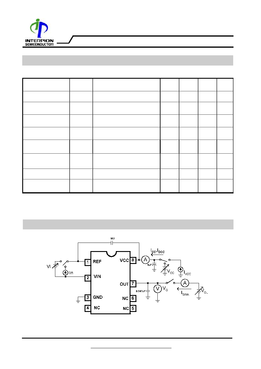
PIN DESCRIPTIONS
PIN CONNECTIONS(PKG)
CHARACTERISTICS
SYMBOL
VALUE
UNIT
Maximum Supply Current
ICCmax
10
mA
Operating Maximum Supply Voltage
VCCmax
20
V
Power Dissipation(8DIP/8SOP)
Pd
800 / 500
mW
REF Pin Current(Note 1)
VIN Pin Bias
100
mA
GND Pin Bias
20
mA
REF Pin Bias
100
mA
GND Pin Bias
20
mA
Operating Junction Temperature
Tj
-30 ~ +80
O
C
Storage Temperature
Tstg
-55 ~ 125
O
C
VIN Pin Current(Note 1)
ABSOLUTE MAXIMUM RATINGS (Ta=25
O
C)
NO
SYMBOL
I/O
DESCRIPTION
1
REF
I
REFERENCE INPUT
2
VIN
I
NEGATIVE INPUT
3
GND
-
GROUND
4
NC
-
NO CONNECTION
5
NC
-
NO CONNECTION
6
NC
-
NO CONNECTION
7
OUT
O
SIGNAL OUTPUT
8
VCC
I
SUPPLY VOLTAGE
Note 1 ; Input Current must be less than 1ms of the pulse width and its duty must be less than 10%.
COB901
Advanced Ground Fault Interrupter
August. 2003(Rev2.)
- 3 -
www.interpionsemi.com
ELECTRICAL CHARACTERISTICS
(Ta = 25
O
C, unless otherwise specified.)
CHARACTERISTICS
SYMBOL
CONDITIONS
MIN
TYP
MAX
UNIT
Supply Current
I
CC
V
CC
=16V,VI=0V
-
350
550
uA
Drive Supply Current
I
DCC
V
CC
=16V,VI=30mV,
Vo=0.7V
-
0.7
1.2
mA
Output
Saturation
Voltage
Vsat
Iv
CC
=2mA,VI=0V
-
-
300
mV
Output Sinking Capa-
bility
Isink
Iv
CC
=2mA,VI=0V, VOL=5V
1.5
3.0
4.5
mA
Trip Voltage(Note 2)
Vtrip
Iv
CC
=2mA,VI=Variable
10
13.5
17
mV
Trip Time
Ttrip
Iv
CC
=2mA,VI=30mV
2
4
6
ms
Output current
Io
Iv
CC
=2mA,VI=30mV
100
250
500
uA
Differential Input
Clamp Voltage
V
DCC
Iin =+/-100mA
0.4
1.1
2.5
V
Note 2 ; Input Voltage Signal(REF,VIN) should be continued more than 6ms.
TEST CIRCUIT

COB901
Advanced Ground Fault Interrupter
August. 2003(Rev2.)
- 4 -
www.interpionsemi.com
TYPICAL APPLICATION
R
s
C
s

COB901
Advanced Ground Fault Interrupter
August. 2003(Rev2.)
- 5 -
www.interpionsemi.com
ELECTRICAL DIAGRAMS
Fig.1 : Supply Current .vs. Temperature
Fig.2 : IDCC vs. Temperature
-40
-20
0
20
40
60
80
100
0
50
100
150
200
250
300
350
400
450
500
Temperature (
o
C)
Test Condition
Vcc=16V,VI=0mV
ICC vs. TEMP
I
C
C
(
u
A
)
-40
-20
0
20
40
60
80
100
400
450
500
550
600
650
700
750
800
850
900
950
1000
Temperature (
o
C)
Test Condition
Vcc=16V,VI=0mV
IDCC vs. TEMP
I
D
C
C
(
u
A
)