- 1 -
Jan. 2005
(Rev.5)
www.interpionsemi.com
IP1117/IP1117-18/IP1117-25/IP1117-33/IP1117-50
LDO Regulator with Adjustable and Fixed 1.8V, 2.5V,3.3V,5.0V
The IP1117 is a series of low dropout voltage regula-
tors which can provide up to 1.0A of output current.
The IP1117 is available in four fixed voltages,
1.8V,2.5V,3.3V and 5.0V. In addition, it is also avail-
able in adjustable version. On chip precision trimming
adjusts the reference/output voltage to within ±2%.
Current limit is also trimmed to ensure specified out-
put current and controlled short-circuit current
The IP1117 series is available in SOT-223 power
packages.
- Adjustable and Fixed of 1.8V, 2.5V, 3.3V,5.0V
- Space saving SMD types of SOT-223
- 1.0A Output Current capability
- 1.1V drop-out voltage
- Foldback current limiting
- Thermal protection
- Over current protection
DESCRIPTION
FEATURES
Device
Package
Operating Temp
IP1117/
IP1117L
SOT-223
IP1117-18/
IP1117L-18
SOT-223
IP1117-25/
IP1117L-25
SOT-223
IP1117-33/
IP1117L-33
SOT-223
IP1117-50/
IP1117L-50
SOT-223
-35
O
C ~ +125
O
C
ORDERING INFORMATION
SOT-223
- Post Regulator for Switching DC/DC Converter
- CD Media
- Battery Charger
- Battery Powered Equipments
APPLICATIONS
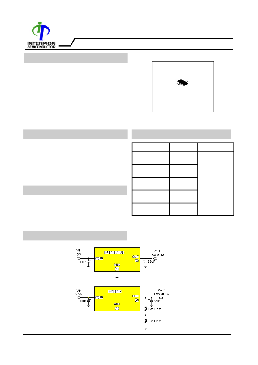
TYPICAL APPLICATION CIRCUITS
L means Lead-free

- 2 -
Jan. 2005
(Rev.5)
www.interpionsemi.com
IP1117/IP1117-18/IP1117-25/IP1117-33/IP1117-50
LDO Regulator with Adjustable and Fixed 1.8V, 2.5V,3.3V,5.0V
PIN DESCRIPTIONS
NO
SYMBOL
I/O
DESCRIPTION
1
ADJ/GND
-
Adjustable or Power Ground
2
OUT
O
Output
3
IN
I
Input
PIN CONNECTIONS
ABSOLUTE MAXIMUM RATINGS
Parameter
Symbol
Value
Units
Input Voltage
Vinmax
18
V
Junction Temperature
Tj
-35 ~ +125
O
C
Storage Temperature
Tstg
-55 ~ +150
O
C
Absolute Maximum Safe Operating Area
Output Current(A)
Vin - Vout (V)
2 4 6 8 10 12 14 16 18 20
0
SOA
0.2
0.4
0.6
0.8
1.0
1.2

- 3 -
Jan. 2005
(Rev.5)
www.interpionsemi.com
IP1117/IP1117-18/IP1117-25/IP1117-33/IP1117-50
LDO Regulator with Adjustable and Fixed 1.8V, 2.5V,3.3V,5.0V
Electrical Characteristics
Parameter
Symbol
Test Conditions
Min.
Typ.
Max.
Units
Reference Voltage
Vref
IP1117 Only
1.5V < (Vin -
Vout) < 7V, Io=10mA
1.225
1.250
1.275
V
Output Voltage
IP1117-18
10mA <
Iout < 1A,
3.3V <
Vin <
10V
1.764
1.800
1.836
V
IP1117-25
10mA < Iout <
1A,
4.0V < Vin <
10V
2.45
2.50
2.55
V
IP1117-33
10mA < Iout <
1A,
4.75V < Vin <
10V
3.234
3.300
3.366
V
IP1117-50
10mA < Iout <
1A,
6.5V < Vin <
12V
4.9
5.0
5.1
V
Line Regulation
dVout1
IP1117
Iout = 10mA,
1.5V <
Vin - Vout <
12V
-
0.035
0.2
%
IP1117-18
Iout = 10mA,
3.3V <
Vin <
15V
-
1
4
mV
IP1117-25
Iout = 10mA,
4.0V <
Vin <
15V
-
1
5
mV
IP1117-33
Iout = 10mA,
4.75V <
Vin <
15V
-
1
7
mV
IP1117-50
Iout = 10mA,
6.5V <
Vin <
15V
-
1
10
mV
Vout
( Vin= 5V, Co=10uF, Ta = 25
O
C, unless otherwise specified.)

- 4 -
Jan. 2005
(Rev.5)
www.interpionsemi.com
IP1117/IP1117-18/IP1117-25/IP1117-33/IP1117-50
LDO Regulator with Adjustable and Fixed 1.8V, 2.5V,3.3V,5.0V
ELECTRICAL CHARACTERISTICS
Parameter
Symbol
Test Conditions
Min.
Typ.
Max.
Units
Load Regulation
IP1117
Vin - Vout =
2.0V,
10mA <
Iout < 1A
-
0.05
0.5
%
IP1117-18
Vin =
3.8V,
10mA <
Iout < 1A
-
1
9
mV
IP1117-25
Vin =
4.5V,
10mA <
Iout < 1A
-
1
12
mV
IP1117-33
Vin =
5.3V,
10mA <
Iout < 1A
-
1
16
mV
IP1117-50
Vin =
7.0V,
10mA <
Iout < 1A
-
1
25
mV
Dropout voltage
Vdrop
Iout = 100mA
-
1.0
1.15
V
Iout = 1A
-
1.1
1.25
V
Quiescent current
Iq
Vin < 12V
-
5
10
mA
Ripple Rejection
RR
f = 120Hz, Cout = 22uF Tantalum,
(Vin-Vout) = 3V, Vripple=1.0Vpp
60
72
-
dB
Current Limit
Ilimit
Vin - Vout =
2V
1
1.5
-
A
Adjust Pin Current
Iadj
-35
-100
uA
Adjust Pin Current
Change
Ichg
10mA <
Iout < 1A
1.5V <
Vin - Vout <
12V
0.2
5
uA
Minimum Load Cur-
rent
Imin
Only IP1117
10
-
-
mA
Long Term Stability
Stable
Ta=125
O
C, 1000hrs
0.03
1.0
%
dVout2
( Vin= 5V, Co=10uF, Ta = 25
O
C, unless otherwise specified.)
- 5 -
Jan. 2005
(Rev.5)
www.interpionsemi.com
IP1117/IP1117-18/IP1117-25/IP1117-33/IP1117-50
LDO Regulator with Adjustable and Fixed 1.8V, 2.5V,3.3V,5.0V
ELECTRICAL CHARACTERISTICS
Parameter
Symbol
Test Conditions
Min.
Typ.
Max.
Units
RMS Output Noise
Vn
10Hz < f < 10kHz
-
0.003
-
%
Thermal Shutdown
Tsd
Junction Temperature
-
150
-
O
C
Thermal Shutdown
Hysteresis
Thys
-
10
-
O
C
( Vin= 5V, Co=10uF, Ta = 25
O
C, unless otherwise specified.)