
August. 2002
(Rev.0)
- 1 -
IP1520
DUAL OUTPUT VOLTAGE SERIES REGULATOR
WWW.INTERPIONSEMI.COM
The IP1520 is a dual output voltage series regulator
which can provide up to 600mA of output current.
The IP1520 consists of 1-fixed 3.3V and 1-fixed 2.55V
regulators.
- 1-Fixed 3.3V Regulator with Internal NPN TR.
- 1-Fixed 2.55V Regulator with Internal NPN TR.
- Built-in TSD circuit.
- Built-in Current Limit Circuit.
- Built-in ON/OFF Control Circuit.
- Built-in Over Voltage Protection Circuit.
- Output Trimmed to +/-3% Tolerance
DESCRIPTION
FEATURES
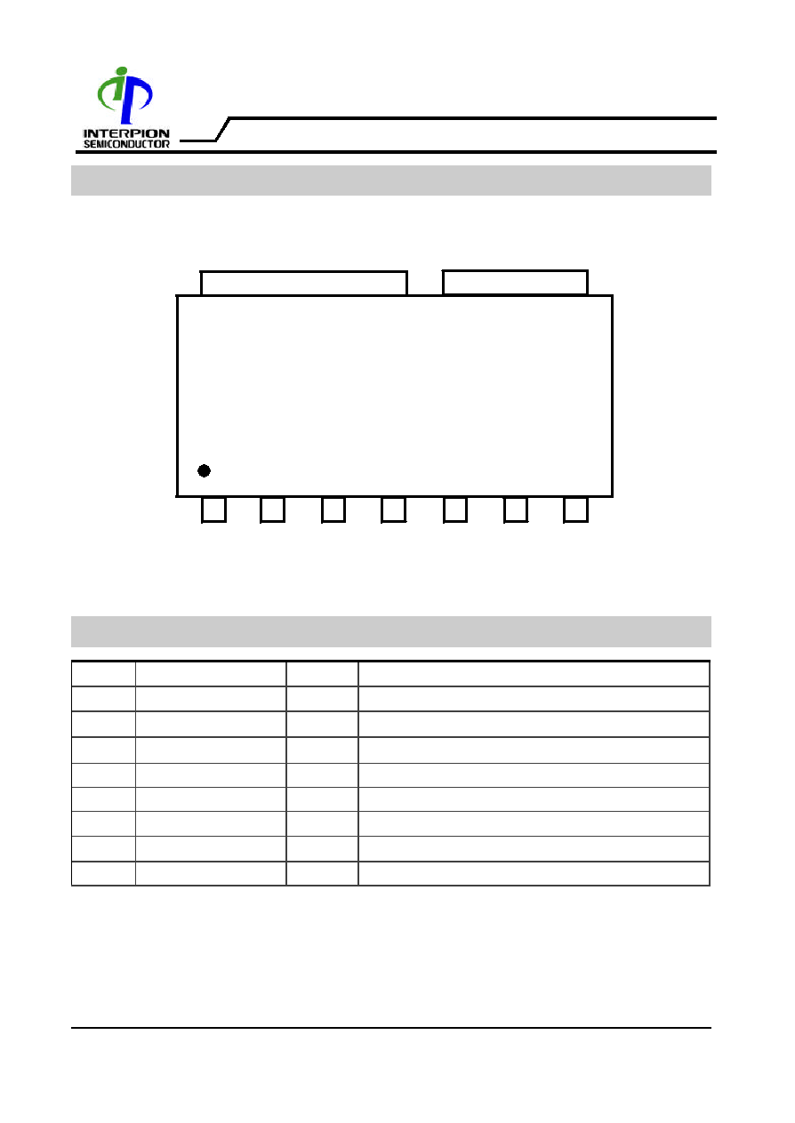
Device
Package
Operating Temp
IP1520
14SOPH-8L
-35
O
C ~ +85
O
C
ORDERING INFORMATION
14SOPH-8L
BLOCK DIAGRAM
N/C
VIN
VOUT1
ON/OFF
PGND
VOUT2
1
2
6
4
5
3
N/C
7
PGND
Vref
ON/OFF
Control SW
TSD
OVP
OCL
N/C
SHUT
DOWN
August. 2002
(Rev.0)
- 2 -
IP1520
DUAL OUTPUT VOLTAGE SERIES REGULATOR
WWW.INTERPIONSEMI.COM
PIN DESCRIPTIONS
NO
SYMBOL
I/O
DESCRIPTION
1
VIN
I
Input Supply Voltage
2
VOUT1
O
Reg +3.3V Output
3
N/C
-
No Connection
4
ON/OFF
I
ON/OFF Control
5
VOUT2
O
Reg +2.55V Output
6
N/C
-
No Connection
7
N/C
-
No Connection
8
PGND
-
Power Ground
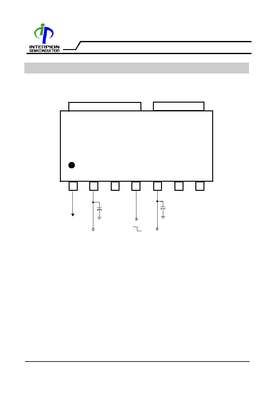
PIN CONNECTIONS
N/C
VIN
VOUT1
ON/OFF
PGND
VOUT2
N/C
PGND
N/C
1
2
6
4
5
3
7
IP1520

August. 2002
(Rev.0)
- 3 -
IP1520
DUAL OUTPUT VOLTAGE SERIES REGULATOR
WWW.INTERPIONSEMI.COM
CHARACTERISTICS
SYMBOL
VALUE
UNIT
Maximum supply voltage
Vinmax
10
V
ON/OFF voltage
Vonoff
10
V
Power dissipation
Pd
3.5*
W
Operating temperature
Topr
-35 ~ +85
O
C
Storage temperature
Tstr
-55 ~ +150
O
C
Maximum output current
Iomax
700
mA
Note>
1. When mounted on 100mm X 100mm X 1mm PCB (Phenolic resin material).
2. Power dissipation reduces 28mW/
O
C for using above Ta=25
O
C
3. Do not exceed Pd and SOA.
POWER DISSIPATION CURVE
Power Dissipation (W)
Ambient Temperature (�C)
25 50 75 100 125 150 175
0
1
2
3
RECOMMENDED OPERATING CONDITIONS
CHARACTERISTICS
SYMBOL
VALUE
UNIT
Supply voltage
Vcc
4.5 ~ 6.0
V
Input voltage
Vin
4.5 ~ 6.0
V
SOA
ABSOLUTE MAXIMUM RATINGS(TA=25
O
C)
4
August. 2002
(Rev.0)
- 4 -
IP1520
DUAL OUTPUT VOLTAGE SERIES REGULATOR
WWW.INTERPIONSEMI.COM
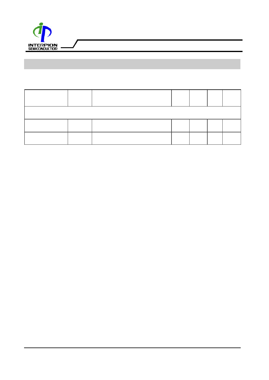
ELECTRICAL CHARACTERISTICS
Characteristics
Symbol
Condition
Min.
Typ.
Max.
Units
Quiescent current
Icc
Vcc=5.25V, No-Load
-
9
14
mA
OVP Detecting
Voltage
Vovp
Vcc=Variable
6.5
-
-
V
3.3V REGULATOR PART
Output Voltage
Vout1
Io=10mA
3.2
3.3
3.4
V
Line Regulation
dVline1 Vin=4.5~6V, Io=10mA
-
0.035
0.2
%
Load Regulation
dVload 1 Vin=5.25V, 10mA < Io < 500mA
-
0.4
0.8
%
Dropout voltage
Vdrop1
Io=500mA
-
1.1
1.3
V
Ripple rejection
RR1
F=120Hz, Co=10uF Tantalum
(Vin-Vout)=3V, Io=200mA
60
70
-
dB
Current limit
*Note
Ilimit1
Vin-Vout=2.5V
550
-
-
mA
Temperature
stability
Temp1
-
-
0.5
-
%
2.55V REGULATOR PART
Output Voltage
Vout2
Io=10mA
2.473
2.55
2.626
V
Line Regulation
dVline2 Vin=4.5~6V, Io=10mA
-
0.035
0.2
%
Load Regulation
dVload2
Vin=5.25V, 10mA < Io < 300mA
-
0.4
0.8
%
Dropout voltage
Vdrop2
Io=300mA
1.7
2.1
V
Ripple rejection
RR2
F=120Hz, Co=10uF Tantalum
(Vin-Vout)=3V, Io=100mA
60
70
dB
Current limit
*Note
Ilimit2
Vin-Vout=3.0V
500
-
-
mA
Temperature
stability
Temp2
-
-
0.5
-
%
Output noise
voltage 1
Vn1
Io=300mA
-
100
-
uV
Output noise
voltage 2
Vn2
Io=150mA
-
100
-
uV
( Vin= 5.25V, Co=10uF, Ta = 25
O
C, unless otherwise specified.)
August. 2002
(Rev.0)
- 5 -
IP1520
DUAL OUTPUT VOLTAGE SERIES REGULATOR
WWW.INTERPIONSEMI.COM
ELECTRICAL CHARACTERISTICS (Continued)
( Vin= 5.25V, Co=10uF, Ta = 25
O
C, unless otherwise specified.)
Parameter
Symbol
Condition
Min.
Typ.
Max.
Units
ON/OFF CONTROL PART
On voltage
Von
Vout=Enabled
-
-
0.8
V
Off voltage
Voff
Vout=Disabled
2.0
-
-
V
* Note
Don't exceed following current limit.
( Iout1 : 550 mA, Iout2 : 500 mA )
August. 2002
(Rev.0)
- 6 -
IP1520
DUAL OUTPUT VOLTAGE SERIES REGULATOR
WWW.INTERPIONSEMI.COM
APPLICATION SUMMARY
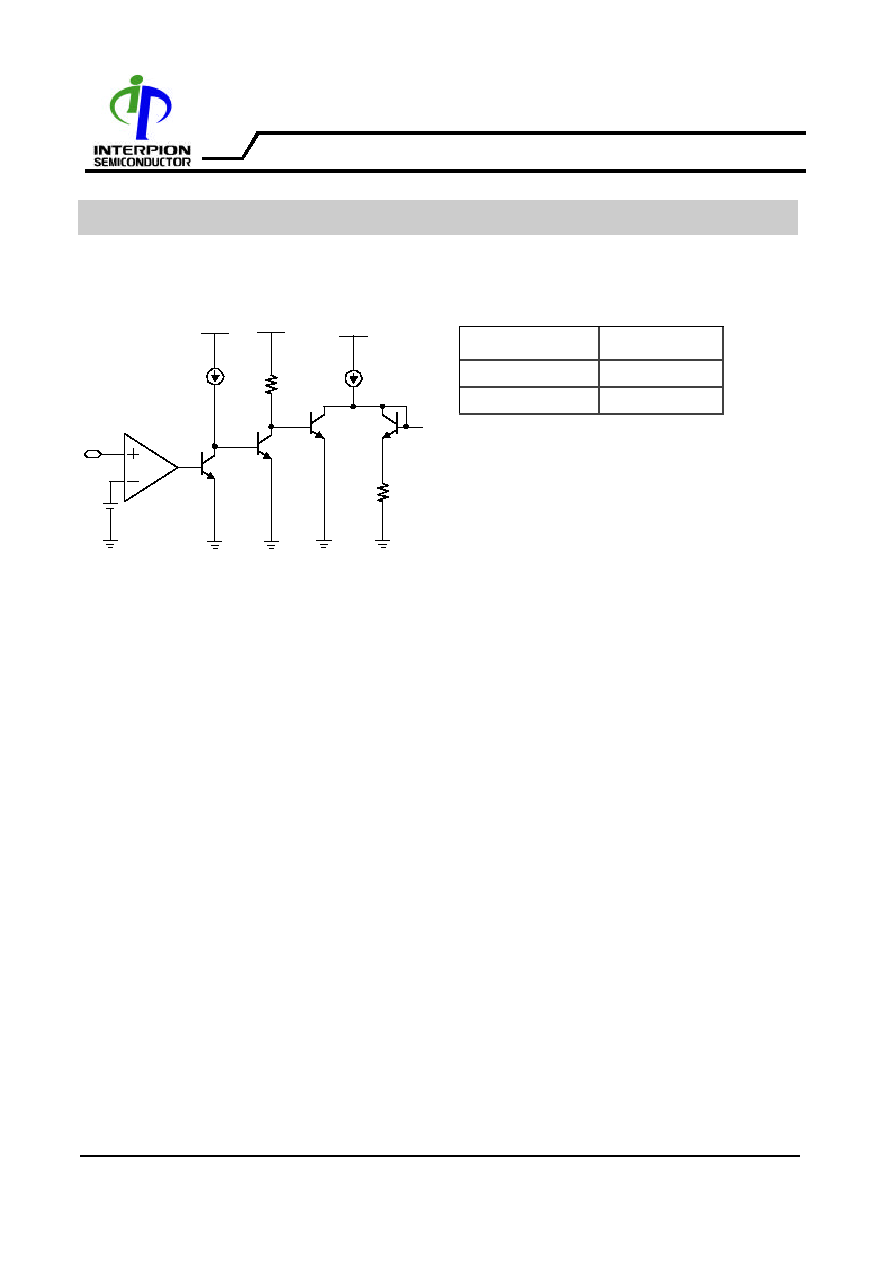
- ON / OFF
When you want to control output of the IP1520, use pin #4 as follows
Pin#4
IP1520
HIGH
off
LOW
on
on/off function
As shown in figure
Pin#4 is positive input of the comparator,
and the other Input is threshold voltage.
If the voltage of the pin#4 rises above threshold voltage,
then TR Q1 will be saturated and the main bias current
will be shut down.
Pin#4
Vth
Main
bias
Q1
August. 2002
(Rev.0)
- 7 -
IP1520
DUAL OUTPUT VOLTAGE SERIES REGULATOR
WWW.INTERPIONSEMI.COM
TYPICAL APPLICATION CIRCUIT
Vinput
2.55V
10uF
10uF
3.3V
N/C
VIN
VOUT1
ON/OFF
PGND
VOUT2
N/C
PGND
N/C
1
2
6
4
5
3
7
IP1520
Von/off
H
L

August. 2002
(Rev.0)
- 8 -
IP1520
DUAL OUTPUT VOLTAGE SERIES REGULATOR
WWW.INTERPIONSEMI.COM
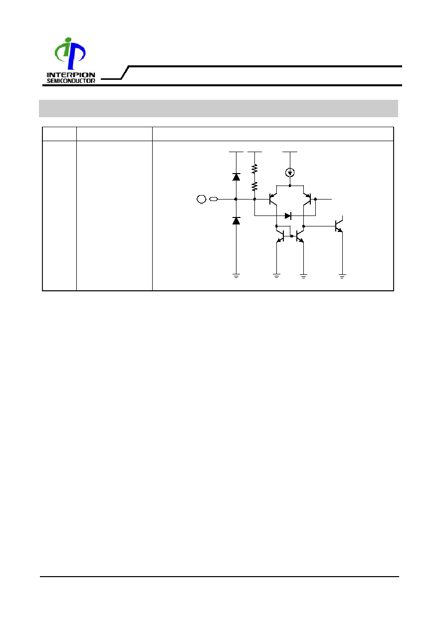
INTERNAL CIRCUIT
Pin no
Pin name
Internal circuit
2
Regulator
output1
5
Regulator
Output2
5
2
August. 2002
(Rev.0)
- 9 -
IP1520
DUAL OUTPUT VOLTAGE SERIES REGULATOR
WWW.INTERPIONSEMI.COM
Pin no
Pin name
Internal circuit
4
ON / OFF
4
INTERNAL CIRCUIT (Continued)
August. 2002
(Rev.0)
- 10 -
IP1520
DUAL OUTPUT VOLTAGE SERIES REGULATOR
WWW.INTERPIONSEMI.COM
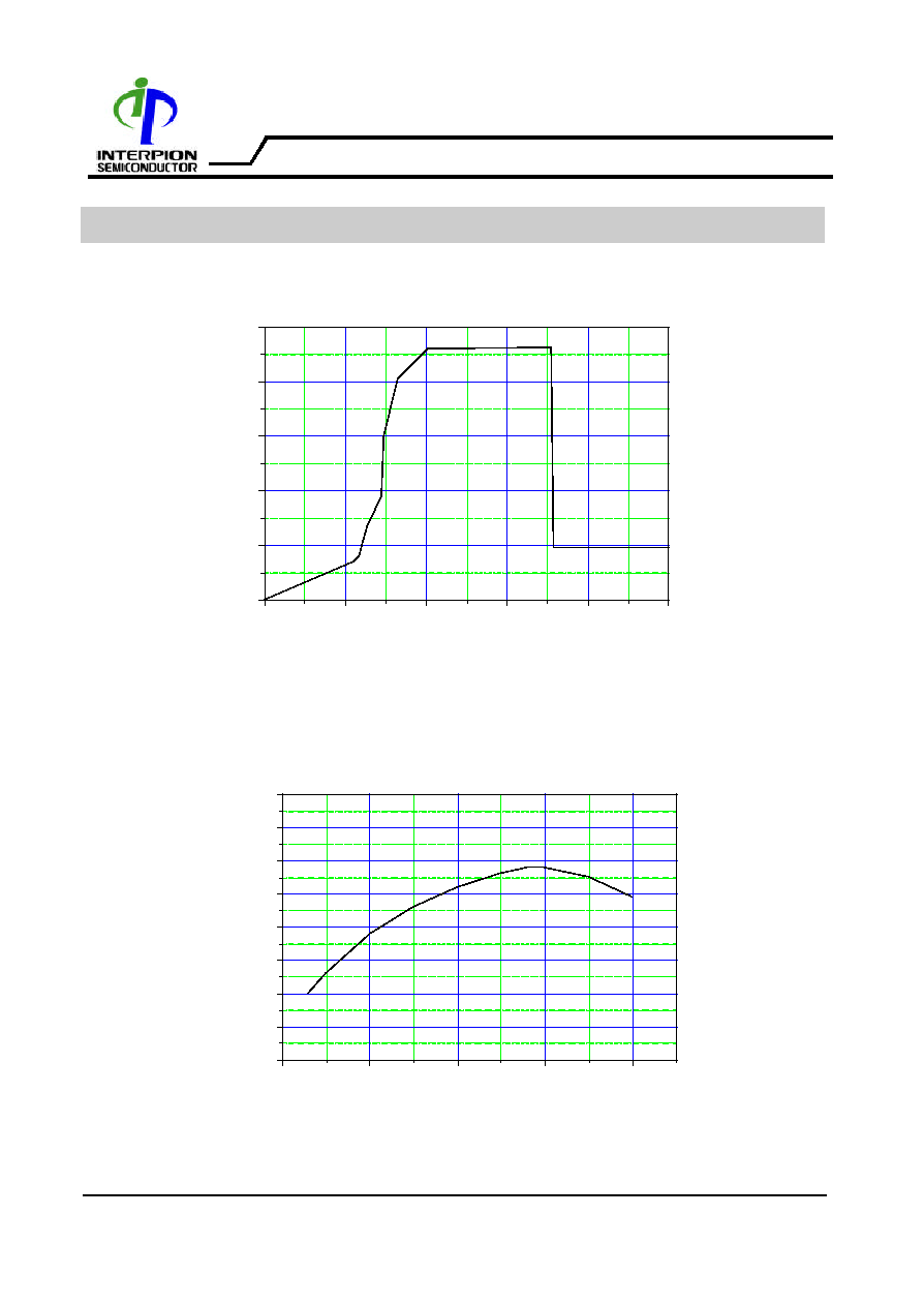
ELECTRICAL CHARACTERISTICS CURVES
0
2
4
6
8
10
0
2
4
6
8
10
VCC vs ICC
Icc (mA)
Vcc (V)
-50
0
50
100
150
1.630
1.635
1.640
1.645
1.650
1.655
1.660
1.665
1.670
VREF TEMPERTURE STABILITY
VREF (V)
TEMP (
O
C)

August. 2002
(Rev.0)
- 11 -
IP1520
DUAL OUTPUT VOLTAGE SERIES REGULATOR
WWW.INTERPIONSEMI.COM
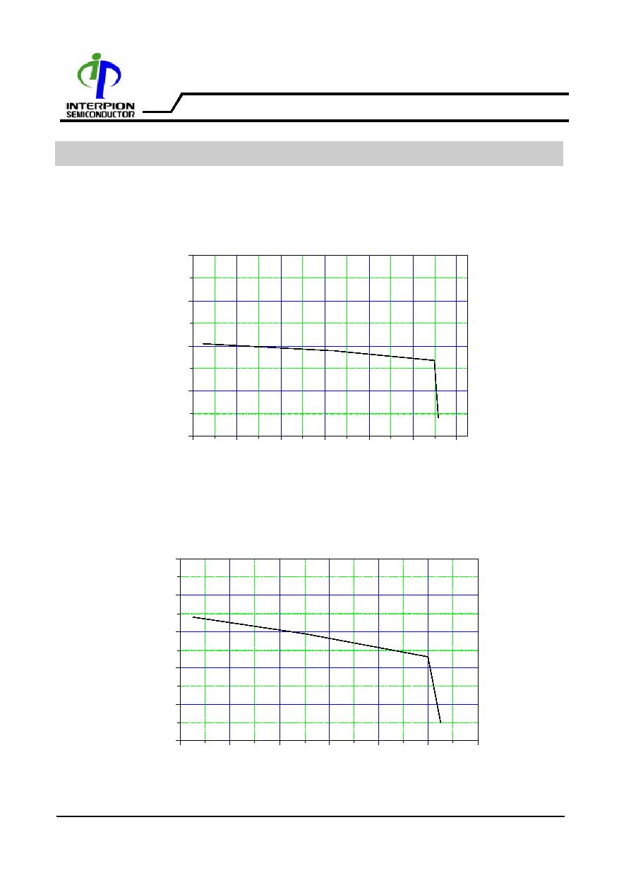
ELECTRICAL CHARACTERISTICS CURVES (Continued)
0
100
200
300
400
500
600
700
800
0.6
0.8
1.0
1.2
1.4
ILoad1 vs Vdrop1
Dropout Voltage1 (V)
Output Current1 (mA)
0
200
400
600
800
1.2
1.4
1.6
1.8
2.0
ILoad2 vs Vdrop2
Dropout Voltage2 (V)
Output Current2 (mA)
August. 2002
(Rev.0)
- 12 -
IP1520
DUAL OUTPUT VOLTAGE SERIES REGULATOR
WWW.INTERPIONSEMI.COM
ELECTRICAL CHARACTERISTICS CURVES (Continued)
0
200
400
600
800
1000
1200
3.20
3.25
3.30
3.35
3.40
VOUT1 Load Regulation (Tj=25
o
C)
Output Voltage1 (V)
Output Current1 (mA)
0
200
400
600
800
1000
1200
2.48
2.50
2.52
2.54
2.56
2.58
VOUT2 Load Regulation (Tj=25
o
C)
Output Voltage (V)
Output Current (mA)

August. 2002
(Rev.0)
- 13 -
IP1520
DUAL OUTPUT VOLTAGE SERIES REGULATOR
WWW.INTERPIONSEMI.COM
ELECTRICAL CHARACTERISTICS CURVES (Continued)
0
20
40
60
80
100
-300
-200
-100
0
100
200
Io=50mA
Io=50mA
Io=450mA
VOUT1 Load Transient Response
Output Voltage Deviation (mV)
Time (usec)
0
20
40
60
80
100
-300
-200
-100
0
100
200
Io=50mA
Io=50mA
Io=350mA
VOUT2 Load Transient Response
Output Voltage Deviation (mV)
Time (usec)

August. 2002
(Rev.0)
- 14 -
IP1520
DUAL OUTPUT VOLTAGE SERIES REGULATOR
WWW.INTERPIONSEMI.COM
PACKAGE DIMENSION
14SOPH-8L
#1
6.00
0.30
(0.236
0.012)
3.95
0.2
(0.156
0.008)
5.72
(0.225)
0.60
0.20
(0.024
0.008)
0.20
+0.10
-0.05
(0.008,+0.004,-0.002)
0~8
0.47
(0.019)
0.406
+0.10
-0.05
(0.008,+0.004,-0.002)
1.27TYP
(0.050TYP)
1.80MAX
(0.071MAX)
MIN0.05
(MIN0.002)
1.55
0.10
(0.061
0.004)
2.946
4.216
8.56
0.20
(
0.347
0.008
)
8.70MAX
(0.343MAX)