
April.2003
(Rev.1)
- 1 -
IP1622
DUAL OUTPUT VOLTAGE LDO REGULATOR + RESET IC
www.interpionsemi.com
- 1-Fixed 3.4V LDO regulator with internal NPN TR.
- 1-Fixed 1.65V LDO regulator with internal NPN TR.
- Typical reset detection voltage of 4.2V.
- Built-in TSD circuit.
- Built-in current limit circuit.
- Built-in over voltage protection circuit.
- Output trimmed to +/-3% tolerance.
DESCRIPTION
FEATURES
Device
Package
Operating Temp
IP1622
14SOPH-8L
-35
O
C ~ +85
O
C
ORDERING INFORMATION
14SOPH-8L
BLOCK DIAGRAM
The IP1620 is an integrated circuit that has triple LDO
regulators and one reset circuit. All the LDO regulators
have their own internal npn power transistors and their
nominal output voltages are 1.65V and 3.4V, respectively.
The reset circuit monitors the status of the regulator input
voltage and outputs the RESET signal. RESET becomes
high after the delay time that is determined by the exter-
nal capacitor at Td pin. The delay time begins to start
after the input voltage reaches above 4.2V.

April.2003
(Rev.1)
- 2 -
IP1622
DUAL OUTPUT VOLTAGE LDO REGULATOR + RESET IC
www.interpionsemi.com
PIN DESCRIPTIONS
NO
SYMBOL
I/O
DESCRIPTION
1
Vin
I
Input Supply Voltage
2
Vdet
I
Detection voltage input
3
Vout1
O
Regulator1 1.65V Output
4
RESET
O
RESET output pin
5
Vout2
O
Regulator2 3.4V Output
6
N/C
-
NO CONNECTION
7
Cd
O
Delay time capacitor pin
8
PGND
-
Power Ground
PIN CONNECTIONS

April.2003
(Rev.1)
- 3 -
IP1622
DUAL OUTPUT VOLTAGE LDO REGULATOR + RESET IC
www.interpionsemi.com
CHARACTERISTICS
SYMBOL
VALUE
UNIT
Maximum supply voltage
Vccmax
10
V
Input voltage
Vinmax
10
V
Power dissipation
Pd
3.0*
W
Operating temperature
Topr
-35 ~ +85
O
C
Maximum output limit current
Io_limit
900
mA
Storage temperature
Tstr
-55 ~ +150
O
C
Note>
1. When mounted on 100mm X 100mm X 1mm PCB (Phenolic resin material).
2. Power dissipation reduces 24mW/
O
C for using above Ta=25
O
C
3. Do not exceed Pd and SOA.
POWER DISSIPATION CURVE
P
o
w
e
r
D
i
s
s
i
p
a
t
i
o
n
(
W
)
Ambient Temperature (
�
C)
25 50 75 100 125 150 175
0
1
2
3
RECOMMENDED OPERATING CONDITIONS
CHARACTERISTICS
SYMBOL
VALUE
UNIT
Supply voltage
VIN
4.5 ~ 6.0
V
SOA
ABSOLUTE MAXIMUM RATINGS(TA=25
O
C)
4
April.2003
(Rev.1)
- 4 -
IP1622
DUAL OUTPUT VOLTAGE LDO REGULATOR + RESET IC
www.interpionsemi.com
ELECTRICAL CHARACTERISTICS
Characteristics
Symbol
Condition
Min.
Typ.
Max.
Units
Quiescent current
Icc
Vcc=5V, No-Load
-
9
15
mA
OVP Dectecting Voltage
Vovp
Vcc=Variable
6.5
7.5
-
V
LDO REGULATOR 1 (1.65V FIXED TYPE)
Output Voltage
Vout1
Io=10mA
1.6
1.65
1.7
V
Line Regulation
dVline1
Vin=4.5~6V, Io=10mA
-
0.035
0.2
%
Load Regulation
dVload 1
Ta=25
O
C
Vin=5V, 10mA < Io < 500mA
-
0.4
1
%
Dropout voltage
Vdrop1
Io=500mA
-
2.5
2.8
V
Ripple rejection
*Note1
RR1
F=120Hz, Co=10uF Tantalum
Vin-Vout=3V, Io=250mA
60
70
-
dB
Current limit
*Note2
Ilimit1
Vin=5V
500
-
-
mA
Temperature
stability
*Note1
Temp1
-
-
0.5
-
%
LDO REGULATOR 2 (3.4V FIXED TYPE)
Output Voltage
Vout2
Io=10mA
3.3
3.4
3.5
V
Line Regulation
dVline2
Vin=4.5~6V, Io=10mA
-
0.035
0.2
%
Load Regulation
dVload 2
Ta=25
O
C
Vin=5V, 10mA < Io < 300mA
-
0.4
1
%
Dropout voltage
Vdrop2
Io=300mA
-
0.9
1.2
V
Ripple rejection
*Note1
RR2
F=120Hz, Co=10uF Tantalum
Vin-Vout=2V, Io=150mA
60
70
-
dB
Current limit
*Note2
Ilimit2
Vin=5V
300
-
-
mA
Temperature
stability
*Note1
Temp2
-
-
0.5
-
%
Noise Voltage
Vn1
f=10Hz~10kHz Io=250mA
-
100
-
uVrms
Noise Voltage
Vn2
f=10Hz~10kHz Io=120mA
-
100
-
uVrms
( Vin= 5V, Co=10uF, Ta = 25
O
C, unless otherwise specified.)

April.2003
(Rev.1)
- 5 -
IP1622
DUAL OUTPUT VOLTAGE LDO REGULATOR + RESET IC
www.interpionsemi.com
ELECTRICAL CHARACTERISTICS
( Vin= 5V, Co=10uF, Ta = 25
O
C, unless otherwise specified.)
Parameter
Symbol
Condition
Min.
Typ.
Max.
Units
RESET PART
Detection voltage
Vd
Vin=L/H/L
4.0
4.2
4.4
V
Td threshold voltage
Vtd
RL=4.7K, Vtd=variable
1.5
1.65
1.8
V
Hysteresis voltage
Vhys
RL=4.7K, Vin=L/H/L
0.2
0.6
0.9
V
Detection reference volt-
age temperature coeff-
cient
*Note1
TCVd
Ta= -20
O
C ~ +85
O
C
-
�
0.01
-
%/
O
C
Reset output current
I
RESET
Vd=0V, V
RESET=
0.4V
3
-
-
mA
High level output voltage
Voh
RL=4.7K
3.8
4.5
4.8
V
Low level output voltage
Vol
RL=4.7K
-
0.1
0.4
V
"
H
"
transport
delay time
tdLH
RL=4.7K, Cd=0.22uF
-
40
-
ms
"
L
"
transport delay time
tdHL
RL=4.7K, Cd=0.22uF
-
50
-
us
* Note1
These parameters are guaranteed, but not 100% tested in mass production.
* Note2
Don
'
t exceed the specified current limit in each output voltage.

April.2003
(Rev.1)
- 6 -
IP1622
DUAL OUTPUT VOLTAGE LDO REGULATOR + RESET IC
www.interpionsemi.com
TYPICAL APPLICATION CIRCUIT

April.2003
(Rev.1)
- 7 -
IP1622
DUAL OUTPUT VOLTAGE LDO REGULATOR + RESET IC
www.interpionsemi.com
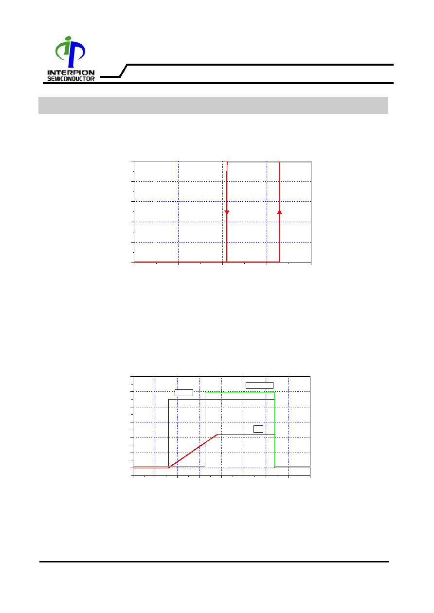
TIMING CHART FOR RESET CIRCUIT

April.2003
(Rev.1)
- 8 -
IP1622
DUAL OUTPUT VOLTAGE LDO REGULATOR + RESET IC
www.interpionsemi.com
Pin no
Pin name
Internal circuit
4
RESET
3,5
Regulator
Output1,2
INTERNAL CIRCUIT

April.2003
(Rev.1)
- 9 -
IP1622
DUAL OUTPUT VOLTAGE LDO REGULATOR + RESET IC
www.interpionsemi.com
ELECTRICAL CHARACTERISTICS CURVES
0
2
4
6
8
10
0
2
4
6
8
10
QUIESCENT CURRENT
I
c
c
(
m
A
)
Vcc (V)
-50
0
50
100
150
1.62
1.63
1.64
1.65
1.66
1.67
VREF TEMPERTURE STABILITY
V
R
E
F
(
V
)
Temp (
o
C)

April.2003
(Rev.1)
- 10 -
IP1622
DUAL OUTPUT VOLTAGE LDO REGULATOR + RESET IC
www.interpionsemi.com
ELECTRICAL CHARACTERISTICS CURVES (Continued)
0
200
400
600
800
1000
1.50
1.55
1.60
1.65
1.70
VOUT1 Load Regulation (Tj=25
o
C)
O
u
t
p
u
t
V
o
l
t
a
g
e
(
V
)
Output Current (mA)
0
200
400
600
3.25
3.30
3.35
3.40
3.45
VOUT2 Load Regulation (Tj=25
o
C)
O
u
t
p
u
t
V
o
l
t
a
g
e
(
V
)
Output Current (m A)

April.2003
(Rev.1)
- 11 -
IP1622
DUAL OUTPUT VOLTAGE LDO REGULATOR + RESET IC
www.interpionsemi.com
ELECTRICAL CHARACTERISTICS CURVES (Continued)
0
20
40
60
80
-200
-100
0
100
200
Io=50mA
Io=500mA
VOUT1 Load Transient Response
O
u
t
p
u
t
V
o
l
t
a
g
e
D
e
v
i
a
t
i
o
n
(
m
V
)
Time (usec)
0
20
40
60
80
-300
-200
-100
0
100
200
Io=50mA
Io=300mA
VOUT2 Load Transient Response
O
u
t
p
u
t
V
o
l
t
a
g
e
D
e
v
i
a
t
i
o
n
(
m
V
)
Time (usec)

April.2003
(Rev.1)
- 12 -
IP1622
DUAL OUTPUT VOLTAGE LDO REGULATOR + RESET IC
www.interpionsemi.com
ELECTRICAL CHARACTERISTICS CURVES (Continued)
0
1
2
3
4
5
0
1
2
3
4
5
Detection Voltage vs. RESETB Voltage
V
R
E
S
E
T
B
(
V
)
Detection Voltage (V)
0
100
200
300
400
500
0.6
0.7
0.8
0.9
1.0
1.1
Dropout Voltage (Vout2=3.4V)
D
r
o
p
o
u
t
V
o
l
t
a
g
e
(
V
)
Output Current (mA)

April.2003
(Rev.1)
- 13 -
IP1622
DUAL OUTPUT VOLTAGE LDO REGULATOR + RESET IC
www.interpionsemi.com
ELECTRICAL CHARACTERISTICS CURVES (Continued)
0
10
20
30
40
3.0
3.5
4.0
4.5
5.0
RESETB High Level Output Voltage
V
R
E
S
E
T
B
(
V
)
Isource (uA)
0
2
4
6
8
10
0.0
0.1
0.2
0.3
0.4
RESETB Low Level Output Voltage
V
R
E
S
E
T
B
(
V
)
Isink (mA)
April.2003
(Rev.1)
- 14 -
IP1622
DUAL OUTPUT VOLTAGE LDO REGULATOR + RESET IC
www.interpionsemi.com
ELECTRICAL CHARACTERISTICS CURVES (Continued)
0.0
0.5
1.0
1.5
2.0
0
1
2
3
4
5
TD Voltage vs. RESETB Voltage
V
R
E
S
E
T
B
(
V
)
TD Voltage (V)
0
25
50
75
100
125
150
175
200
0
1
2
3
4
5
6
RESETB
TD
VDET
RESET IC Tim ing Chart
V
o
l
t
a
g
e
(
V
)
Tim e (m sec)

April.2003
(Rev.1)
- 15 -
IP1622
DUAL OUTPUT VOLTAGE LDO REGULATOR + RESET IC
www.interpionsemi.com
PACKAGE DIMENSION
14SOPH-8L
#1
6.00
0.30
(0.236
0.012)
3.95
0.2
(0.156
0.008)
5.72
(0.225)
0.60
0.20
(0.024
0.008)
0~8
1.80MAX
(0.071MAX)
MIN0.05
(MIN0.002)
1.55
0.10
(0.061
0.004)