June. 2005
(Rev. 3)
- 1 -
IP9009
5-CH Motor Drive IC with Regulator and Reset controllers
www.interpionsemi.com
IP9009 is a 5-CH motor driver with LDO regulator and
reset controller. It is suitable for CD-P/VCD-P/DVD-P
systems. The motor driver part is composed of four BTL
drivers and one forward/reverse controlled DC motor
driver.
- 4-CH BTL driver.
- 1-CH forward/reverse controlled DC motor driver.
- Built-in adjustable LDO regulator controller.
- Built-in reset controller.
- Built-in TSD (thermal shut down) circuit.
- Built-in mute circuit.
- Built-in power save circuit.
DESCRIPTIONS
ORDER INFORMATION
FEATURES
28SSOPH-375B
Device
Package
Operating
Temp
IP9009
28SSOPH-375A
-35
O
C ~ +85
O
C
IP9009-TF
28SSOPH-375A
-35
O
C ~ +85
O
C
IP9009L
28SSOPH-375A
-35
O
C ~ +85
O
C
IP9009L-TF
28SSOPH-375A
-35
O
C ~ +85
O
C
IP9009
28SSOPH-375B
-35
O
C ~ +85
O
C
IP9009-TF
28SSOPH-375B
-35
O
C ~ +85
O
C
IP9009L
28SSOPH-375B
-35
O
C ~ +85
O
C
IP9009L-TF
28SSOPH-375B
-35
O
C ~ +85
O
C
* L : Lead Free
* TF : Tape & Reel packing
* L-TF : Lead Free and Tape & Reel packing
June. 2005
(Rev. 3)
- 2 -
IP9009
5-CH Motor Drive IC with Regulator and Reset controllers
www.interpionsemi.com
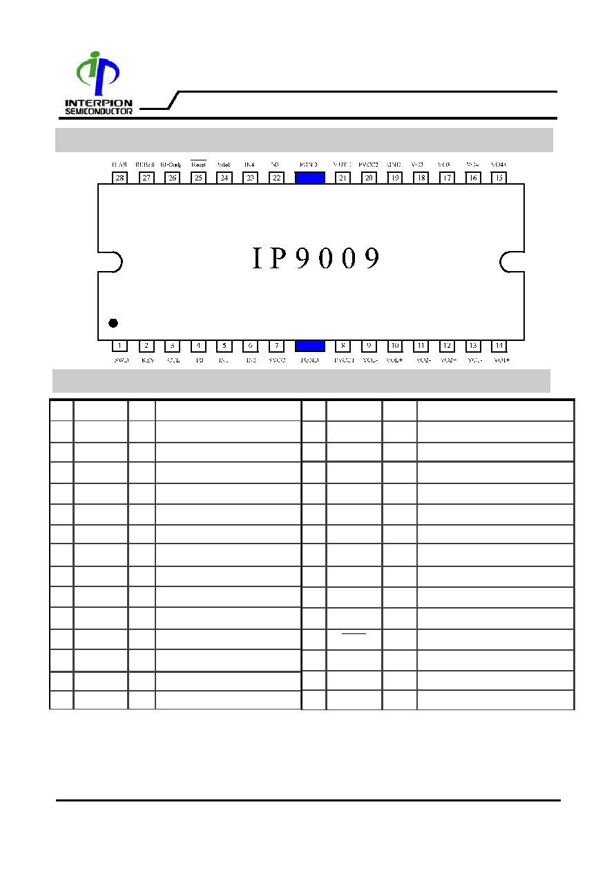
PIN DESCRIPTIONS
PIN CONNECTIONS
NO SYMBOL I/O DESCRIPTION
1
FWD
I
Loading motor forward input
2
REV
I
Loading motor reverse input
3
CTL
I
Loading motor speed control
4
PS
I
Power save
5
IN1
I
CH1 input
6
IN2
I
CH2 input
7
SVCC
-
Signal power supply
8
PVCC1
-
Power supply 1
9
VOL-
O Loading driver output(-)
10
VOL+
O Loading driver output(+)
11
VO2-
O CH2 driver output(-)
12
VO2+
O CH2 driver output(+)
13
VO1-
O CH1 driver output(-)
14
VO1+
O CH1 driver output(+)
NO SYMBOL
I/O DESCRIPTION
15
VO4+
O
CH4 driver output(+)
16
VO4-
O
CH4 driver output(-)
17
VO3+
O
CH3 driver output(+)
18
VO3-
O
CH3 driver output(-)
19
GND
-
Ground
20
PVCC2
-
Power supply 2
21
MUTE
I
Mute
22
IN3
I
CH3 input
23
IN4
I
CH4 input
24
Vdet
I
Reset controller input
25
Reset
O
Reset controller output
26
REOadj
O
Adjustable regulator feedback
27
REBadj
O
Adjustable regulator control
28
BIAS
I
Bias
June. 2005
(Rev. 3)
- 3 -
IP9009
5-CH Motor Drive IC with Regulator and Reset controllers
www.interpionsemi.com
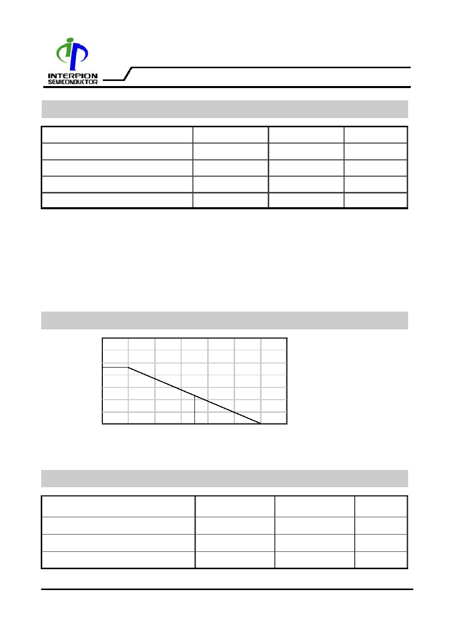
CHARACTERISTICS
SYMBOL
VALUE
UNIT
Maximum supply voltage
VCCmax
V
Power dissipation
Pd
2.3 *
W
Operating temperature
Topr
-35 ~ +85
O
C
Storage temperature
Tstg
-55 ~ 150
O
C
15
Note>
1. When mounted on 50mm X 50mm X 1mm PCB (Phenolic resin material).
2. Power dissipation reduces 18.4 mW/
O
C for using above Ta=25
O
C
3. Do not exceed Pd and SOA.
POWER DISSIPATION CURVE
RECOMMENDED OPERATING CONDITIONS
CHARACTERISTICS
SYMBOL
VALUE
UNIT
Signal supply Voltage
SVCC
4.3 ~ 13.2
V
Power supply Voltage 2
PVCC2
4.3 ~ SVCC
V
Power supply Voltage 1
PVCC1
4.3 ~ SVCC
V
ABSOLUTE MAXIMUM RATINGS
P
o
w
e
r
D
i
s
s
i
p
a
t
i
o
n
(
m
W
)
Ambient Temperature (�C)
25 50 75 100 125 150 175
0
1
2
3

June. 2005
(Rev. 3)
- 4 -
IP9009
5-CH Motor Drive IC with Regulator and Reset controllers
www.interpionsemi.com
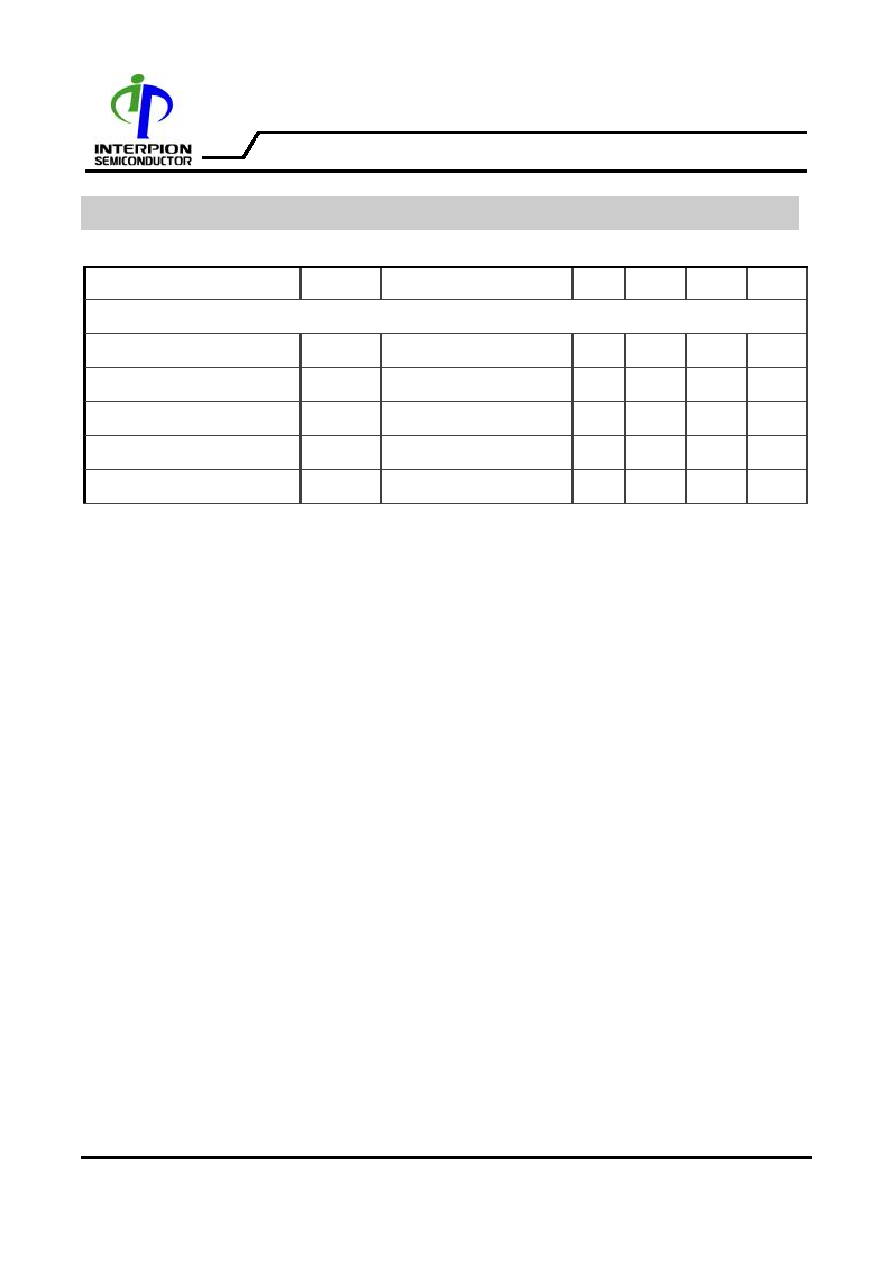
ELECTRICAL CHARACTERISTICS
CHARACTERISTICS
SYMBOL CONDITIONS
MIN
TYP
MAX
UNIT
Quiescent circuit current
Icc
No Load
-
20
30
mA
Power save on current
Ips
Pin5=GND
-
0.5
2.0
mA
Power save on voltage
Vpson
Pin5=sweep
-
-
0.5
V
Power save off voltage
Vpsoff
Pin5=sweep
2.0
-
-
V
[ ADJUSTABLE REGULATOR PART ]
Output voltage
V
REG
IL=100mA
Vout*
0.95
Vout
Vout*
1.05
V
Load Regulation
Vom
IL=0->200mA
-50
0
50
mV
Line Regulation
Vcc
Vcc=6->10V,IL=100mA
-50
0
50
mV
[ RESET CONTROLLER PART ]
Detecting voltage
Vdet
Pin24=sweep (low->high)
2.6
2.9
3.2
V
Hysteresis voltage
Vdet
-
50
-
mV
Maximum output sink current
Isink
3
6
-
mA
Output saturation voltage
Vsat
RL=1k ohm
-
-
0.4
V
Output offset voltage
Voos
Vin=Vref
-100
-
+100
mV
Maximum output voltage
Voms
3.6
4.0
-
V
Closed-loop voltage gain
Avfs
Vin=0.1Vrms, f=1kHz
17
19
21
dB
Mute on voltage
Vmon
Pin21=sweep
-
-
0.5
V
Mute off voltage
Vmoff
Pin21=sweep
1.5
-
-
V
Mute pin current
Imp
Pin21=5.0V
200
300
uA
Bias pin current
Ibias
Pin28=2.5V
80
120
uA
[ BTL DRIVE PART ]
(SVCC=12.0V,PVCC1=PVCC2=5V, RL=12ohm, Bias=1.65V, Ta = 25
O
C unless otherwise specified.)
June. 2005
(Rev. 3)
- 5 -
IP9009
5-CH Motor Drive IC with Regulator and Reset controllers
www.interpionsemi.com
ELECTRICAL CHARACTERISTICS
CHARACTERISTICS
SYMBOL CONDITIONS
MIN
TYP
MAX
UNIT
[ LOADING DRIVER PART ]
Input high level voltage
Vih
1.5
-
-
V
Input low level voltage
Vil
-
-
0.5
V
FWD/REV pin current
Iin
Pin1=Pin2=5.0V
-
200
300
uA
Maximum output voltage
Vo
RL=25 ohm
9.0
10
-
V
Voltage gain
Gvf
Pin3=sweep
7
9
11
dB
(SVCC=12.0V,PVCC1=PVCC2=5V, RL=12ohm, Bias=1.65V, Ta = 25
O
C unless otherwise specified.)