 | –≠–ª–µ–∫—Ç—Ä–æ–Ω–Ω—ã–π –∫–æ–º–ø–æ–Ω–µ–Ω—Ç: G913A | –°–∫–∞—á–∞—Ç—å:  PDF PDF  ZIP ZIP |

Ver 0.9 Preliminary
Jan 25, 2002
TEL: 886-3-5788833
http://www.gmt.com.tw
1
G913
Global Mixed-mode Technology Inc.
150mA Low-Dropout Linear Regulators
Features
Low, 55µA No-Load Supply Current
Guaranteed 150mA Output Current
Dropout Voltage is 70mV @ 50mA Load
Over-Temperature Protection and Short-Circuit
Protection
Two Modes of Operation ----
Fixed Mode: 2.84V (G913A), 3.15V (G913B),
3.30V (G913C), 3.00V (G913D)
Adjustable Mode: from 1.25V to 5.5V
Max. Supply Current in Shutdown Mode < 1µA
Low Output Noise at 220µV
RMS
Stability with lost cost ceramic capacitors
Applications
Notebook Computers
Cellular Phones
PDAs
Digital still Camera and Video Recorders
Hand-Held Devices
Bar Code Scanners
General
Description
The G913 is a low supply current, low dropout linear
regulator that comes in a space saving SOT23-5 pack-
age. The supply current at no-load is 55µA. In the
shutdown mode, the maximum supply current is less
than 1µA. Operating voltage range of the G913 is from
2.5V to 5.5V. The over-current protection limit is set at
250mA typical and 150mA minimum. An overtem-
perature protection circuit is built-in in the G913 to
prevent thermal overload. These power saving fea-
tures make the G913 ideal for use in the bat-
tery-powered applications such as notebook com-
puters, cellular phones, and PDA's.
The G913 has two modes of operation. When the SET
pin is connected to ground, its output is a pre-set
value: 2.84V for G913A, 3.15V for G913B, and 3.30V
for G913C, and 3.00V for G913D. There is no external
components needed to decide the output voltage.
When an output other than the preset value is needed,
two external resistors should be used as a voltage
divider. The output voltage is then decided by the re-
sistor ratio. The G913 comes in a space saving
SOT23-5 package.
Ordering Information
PART MARKING VOLTAGE
TEMP.
RANGE
PIN-
PACKAGE
G913A
3A
2.84
-40∞C~ +85∞C
SOT 23-5
G913B
3B
3.15
-40∞C~ +85∞C
SOT 23-5
G913C
3C
3.30
-40∞C~ +85∞C
SOT 23-5
G913D
3D
3.00
-40∞C~ +85∞C
SOT 23-5
Pin Configuration
G963
SET
OUT
SOT23-5
G913
5
4
1
SHDN
2
3
GND
IN
IN
OUT
SHDN
SET
GND
G913
BATTERY C
IN
1µF
R1
R2
C
OUT
1µF
OUTPUT
VOLTAGE
Adjustable mode
IN
OUT
GND
SET
SHDN
G913
C
IN
1µF
_
BATTERY
OUTPUT
VOLTAGE
C
OUT
1
µ
F
Fixed mode
G963
SET
OUT
SOT23-5
G913
5
4
1
SHDN
2
3
GND
IN
G963
SET
OUT
SOT23-5
G913
5
4
1
SHDN
2
3
GND
IN
IN
OUT
SHDN
SET
GND
G913
BATTERY C
IN
1µF
R1
R2
C
OUT
1µF
OUTPUT
VOLTAGE
Adjustable mode
IN
OUT
GND
SET
SHDN
G913
C
IN
1µF
_
BATTERY
OUTPUT
VOLTAGE
C
OUT
1
µ
F
Fixed mode
IN
OUT
SHDN
SET
GND
G913
BATTERY C
IN
1µF
R1
R2
C
OUT
1µF
OUTPUT
VOLTAGE
Adjustable mode
IN
OUT
GND
SET
SHDN
G913
C
IN
1µF
_
BATTERY
OUTPUT
VOLTAGE
C
OUT
1
µ
F
Fixed mode

Ver 0.9 Preliminary
Jan 25, 2002
TEL: 886-3-5788833
http://www.gmt.com.tw
2
G913
Global Mixed-mode Technology Inc.
Absolute Maximum Ratings
V
IN
to GND..........................................-0.3V to +7V
Output Short-Circuit Duration..........................Infinite
SET to GND.........................................-0.3V to +7V
SHDN to GND....................................-0.3V to +7V
SHDN to IN.........................................-7V to +0.3V
OUT to GND..............................-0.3V to (V
IN
+ 0.3V)
Continuous Power Dissipation (T
A
= +25∞C)
SOT23-5..................................................520 mW
Operating Temperature Range............-40∞C to +85∞C
Junction Temperature..................................+150∞C
JA
(1)
...................................................240∞C/Watt
Storage Temperature Range.............-65∞C to +160∞C
Lead Temperature (soldering, 10sec)..............+300∞C
Note (1): See Recommended Minimum Footprint (Figure 3)
Stresses beyond those listed under "Absolute Maximum Ratings" may cause permanent damage to the device. These are stress rat-
ings only, and functional operation of the device at these or any other conditions beyond those indicated in the operational sections of
the specifications is not implied. Exposure to absolute maximum rating conditions for extended periods may affect device reliability.
Electrical Characteristics
(V
IN
=+3.6V, V
SHDN
=V
IN
, T
A
=T
J
=+25∞C, unless otherwise noted.) (Note 1)
PARAMETER SYMBOL CONDITIONS MIN
TYP
MAX
UNITS
Input Voltage (Note 2)
V
IN
2.5
5.5
V
Output Voltage Accuracy
V
OUT
Variation from specified V
OUT
, I
OUT
=1mA -2
2
%
Adjustable Output Voltage Range (Note 3)
V
OUT
V
SET
5.5 V
Maximum Output Current
150
mA
Current Limit (Note 4)
I
LIM
250
mA
I
LOAD
= 0mA
55
120
Ground Pin Current
I
Q
SET = GND
I
LOAD
= 50mA
145
µA
I
OUT
= 1mA
2
I
OUT
= 50mA
70
Dropout Voltage (Note 5)
V
DROP
I
OUT
=150mA
230 300
mV
SET=GND, V
IN
=V
(STD)
+0.1V,to 5.5V I
OUT
= 1mA
0.1 0.28
Line Regulation
V
LNR
SET tied to OUT, V
IN
=2.5V to 5.5V, I
OUT
= 1mA
0.08 0.4
%/V
SET tied to OUT
0.02 0.8
Load Regulation
V
LDR
I
OUT
= 0mA to 150mA
SET = GND
1.0
%
Output Voltage Noise (10Hz to 100kHz)
e
n
V
IN
=4.2V,
I
OUT
=150mA
C
OUT
= 1µF
220
µV
RMS
SHUTDOWN
V
IH
Regulator
enabled
V
IN
-0.7
SHDN
Input Threshold
V
IL
Regulator
shutdown
0.4
V
SHDN
Input Bias Current
I
SHDN
V
SHDN
= V
IN
T
A
= +25∞C
0.003
0.1 µA
Shutdown Supply Current
I
QSHDN
V
OUT
= 0V
T
A
= +25∞C
0.2
1
µA
SET INPUT
T
A
= +25∞C
1.225 1.25 1.275
SET Reference Voltage (Note 3)
V
SET
V
IN
= 2.5V to 5.5V,
I
OUT
= 1mA
T
A
= T
MIN
to T
MAX
1.25
V
SET Input Leakage Current (Note 3)
I
SET
V
SET
= 1.3V
T
A
= +25∞C
5
30
nA
THERMAL PROTECTION
Thermal Shutdown Temperature
T
SHDN
150
∞C
Thermal Shutdown Hysteresis
T
SHDN
15
∞C
Note 1: Limits is 100% production tested at T
A
= +25∞C. Low duty pulse techniques are used during test to
maintain junction temperature as close to ambient as possible.
Note 2: Guaranteed by line regulation test.
Note 3: Adjustable mode only.
Note 4: Not tested. For design purposes, the current limit should be considered 150mA minimum to 420mA maximum.
Note 5: The dropout voltage is defined as (V
IN
-V
OUT
) when V
OUT
is 100mV below the value of V
OUT
for V
IN
= V
OUT
+2V,
The performance of every G913 part, see "Typical Performance Characteristics".
Ver 0.9 Preliminary
Jan 25, 2002
TEL: 886-3-5788833
http://www.gmt.com.tw
3
G913
Global Mixed-mode Technology Inc.
Typical Performance Characteristics
(V
IN
= +3.6V, C
IN
=1µF, C
OUT
=1µF, G913B, T
A
=25 ∞C, unless otherwise noted.)
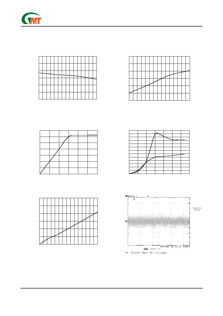
Output Voltage vs. Load Current
Ground Current vs. Load Current
Output Voltage vs. Load Current
Supply Current vs. Input Voltage
Dropout Voltage vs. Load Current
Output Noise 10HZ to 100KHZ
0
10
20
30
40
50
60
70
80
90
100
110
120
130
0
1
2
3
4
5
6
7
Input Voltage (V)
Supply Current (
A)
I
LOAD
= 0A
I
LOAD
= 50mA
0.00
0.50
1.00
1.50
2.00
2.50
3.00
3.50
0
1
2
3
4
5
6
Input Voltage (V)
Output Voltage (V)
No Load
0
50
100
150
200
250
300
0
10 20 30 40 50 60 70 80 90 100 110 120 130 140 150
Load Current (mA)
Ground Current (
A)
3.100
3.110
3.120
3.130
3.140
3.150
3.160
0
10 20 30 40 50 60 70 80 90 100 110 120 130 140 150
Load Current (mA)
Output Voltage (V)
0
50
100
150
200
250
300
0
10 20 30 40 50 60 70 80 90 100 110 120 130 140 150
Load Current (mA)
Dropout Voltage (mV)
Ver 0.9 Preliminary
Jan 25, 2002
TEL: 886-3-5788833
http://www.gmt.com.tw
4
G913
Global Mixed-mode Technology Inc.
Typical Performance Characteristics
(V
IN
= +3.6V, C
IN
=1µF, C
OUT
=1µF, G913B, T
A
=25 ∞C, unless otherwise noted.)
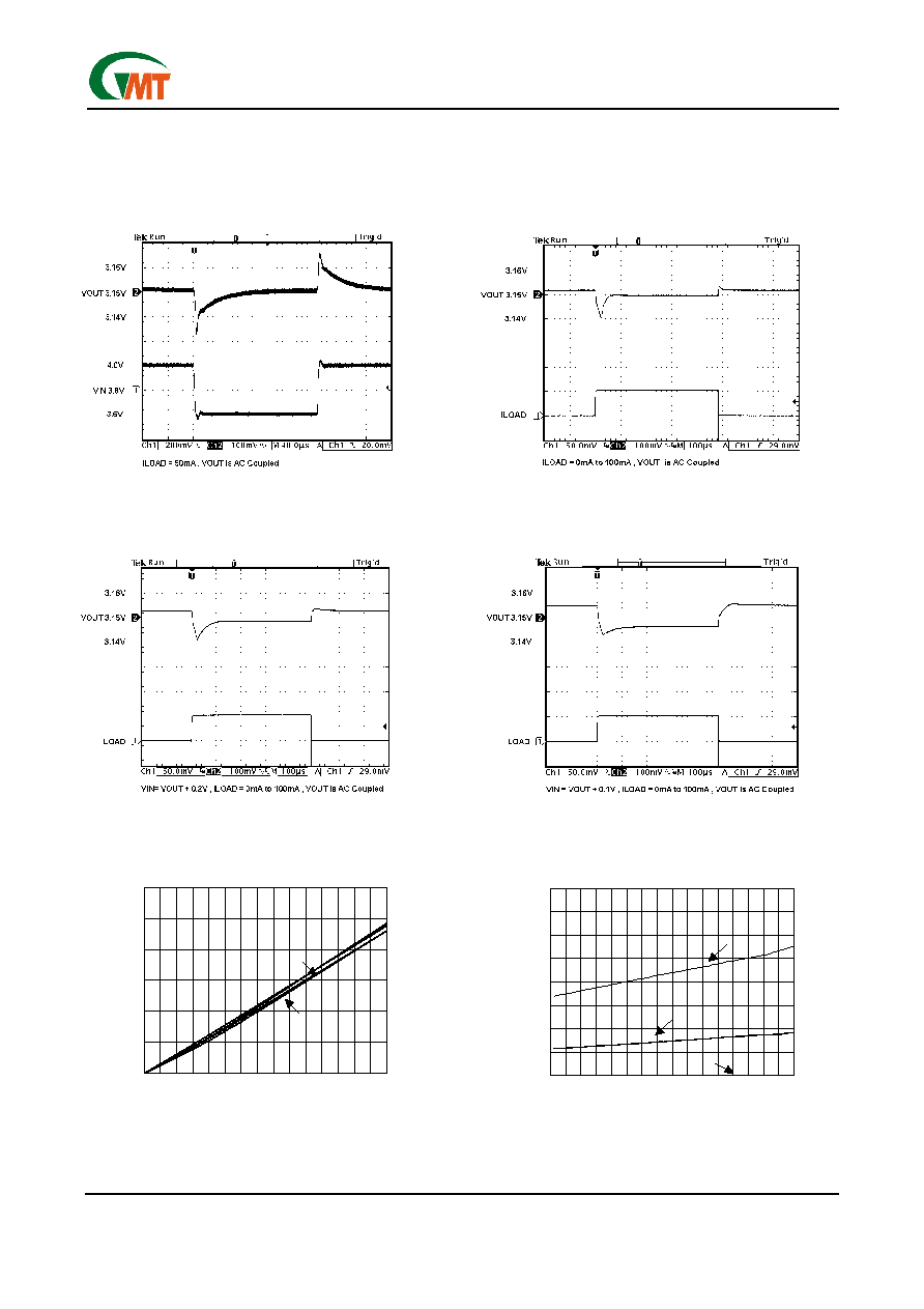
Dropout Voltage vs. Load Current by G913
Load Transient
Dropout Voltage vs. Temperature
Line Transient
Load Transient
Load Transient
0
50
100
150
200
250
300
0
10 20 30 40 50 60 70 80 90 100 110 120 130 140 150
Load Current (mA)
Dropout Voltage (mV)
T
A
=25∞C
Top to Bottom
G913C
G913B
G913D
G913A
0
50
100
150
200
250
300
350
400
-40 -30 -20 -10
0
10
20
30
40
50
60
70
80
90 100 110 120
Junction Temperature T
J
(
)
Dropout Voltage (mV)
G913C
I
LOAD
=150mA
I
LOAD
=50mA
I
LOAD
=0mA

Ver 0.9 Preliminary
Jan 25, 2002
TEL: 886-3-5788833
http://www.gmt.com.tw
5
G913
Global Mixed-mode Technology Inc.
Typical Performance Characteristics
(V
IN
= +3.6V, C
IN
=1µF, C
OUT
=1µF, G913B, T
A
=25 ∞C, unless otherwise noted.)
Shutdown Pin Delay
Shutdown Response Time
Shutdown Pin Delay
Turn on Response Time
Turn off Response Time
Shutdown Response Time

Ver 0.9 Preliminary
Jan 25, 2002
TEL: 886-3-5788833
http://www.gmt.com.tw
6
G913
Global Mixed-mode Technology Inc.
Typical Performance Characteristics
(V
IN
= +3.6V, C
IN
=1µF, C
OUT
=1µF, G913B, T
A
=25 ∞C, unless otherwise noted.)
Output Voltage vs. Temperature
Ground Current vs. Temperature
Shutdown Supply Current
SHDN Input Bias Current vs. Temperature
SET Input Leakage Current vs. Temperature
SET Reference Voltage vs. Temperature
-0.20
-0.10
0.00
0.10
0.20
-40
-30
-20
-10
0
10
20
30
40
50
60
70
80
90
100 110 120
Junction Temperature T
J
(
)
SHDN Input Bias Current (
A)
-1.00
-0.80
-0.60
-0.40
-0.20
0.00
0.20
0.40
0.60
0.80
1.00
-40 -30 -20
-10
0
10
20
30
40
50
60
70
80
90
100 110 120
Junction Temperature T
J
(
)
Shutdown Supply Current (
A)
-10
-5
0
5
10
15
20
25
30
35
40
45
50
55
60
-40
-30 -20 -10
0
10
20
30
40
50
60
70
80
90
100 110 120
Junction Temperature T
J
(
)
SET Input Leakage Current (nA)
3.280
3.290
3.300
3.310
3.320
3.330
3.340
-40 -30 -20 -10
0
10
20
30
40
50
60
70
80
90
100 110 120
Junction Temperature T
J
(
)
Output Voltage (V)
G913C
G913C
G913C
V
IN
=3.6V
G913C
I
LOAD
=1mA
V
IN
=5.5V
V
IN
=3.4V
0
20
40
60
80
100
-40
-30
-20
-10
0
10
20
30
40
50
60
70
80
90
100 110 120
Junction Temperature T
J
(
)
Ground Current (
A)
G913C
I
LOAD
=0A
1.230
1.235
1.240
1.245
1.250
1.255
1.260
-40
-30
-20
-10
0
10
20
30
40
50
60
70
80
90
100 110 120
Junction Temperature T
J
(
)
SET Reference Voltage (V)
G913C
I
LOAD
=1mA
V
IN
=5.5V
V
IN
=2.5V
V
IN
=3.6V
Ver 0.9 Preliminary
Jan 25, 2002
TEL: 886-3-5788833
http://www.gmt.com.tw
7
G913
Global Mixed-mode Technology Inc.
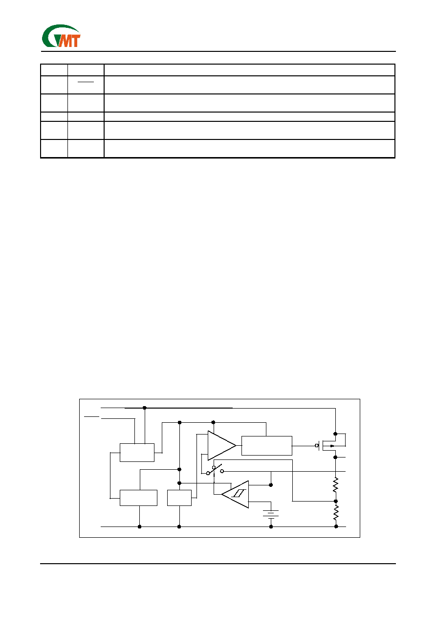
Pin Description
PIN
NAME
FUNCTION
1
SHDN
Active-Low Shutdown Input. A logic low reduces the supply current to less than 1
µ
A. Connect to IN for normal
operation.
2 GND
Ground. This pin also functions as a heatsink. Solder to large pads or the circuit board ground plane to
maximize thermal dissipation.
3
IN
Regulator Input. Supply voltage can range from +2.5V to +5.5V. Bypass with 1µF to GND
4 OUT
Regulator Output. Fixed or adjustable from 1.25V to +5.5V. Sources up to 150mA. Bypass with a 1µF,
0.2
typical ESR capacitor to GND.
5 SET
Feedback Input for Setting the Output Voltage. Connect to GND to set the output voltage to the preset
2.84V or 3.15V or 3.30V or 3.00V. Connect to an external resistor divider for adjustable-output operation.
Detailed Description
The block diagram of the G913 is shown in Figure 1. It
consists of an error amplifier, 1.25V bandgap refer-
ence, PMOS output transistor, internal feedback volt-
age divider, mode comparator, shutdown logic, over
current protection circuit, and over temperature protec-
tion circuit.
The mode comparator compares the SET pin voltage
with an internal 120mV reference. If the SET pin volt-
age is less than 120mV, the internal feedback voltage
divider's central tap is connected to the non-inverting
input of the error amplifier. The error amplifier com-
pares non-inverting input with the 1.25V bandgap ref-
erence. If the feedback voltage is higher than 1.25V,
the error amplifier's output becomes higher so that the
PMOS output transistor has a smaller gate-to-source
voltage (V
GS
). This reduces the current carrying capa-
bility of the PMOS output transistor, as a result the
output voltage decreases until the feedback voltage is
equal to 1.25V. Similarly, when the feedback voltage
is less than 1.25V, the error amplifier causes the out-
put PMOS to conductor more current to pull the feed-
back voltage up to 1.25V. Thus, through this feedback
action, the error amplifier, output PMOS, and the volt-
age divider effectively form a unity-gain amplifier with
the feedback voltage force to be the same as the
1.25V bandgap reference. The output voltage, V
OUT
, is
then given by the following equation:
V
OUT
= 1.25 (1 + R1/R2).
(1)
Alternatively, the relationship between R1 and R2 is
given by:
R1 = R2 (V
OUT
/1.25 + 1).
(2)
For the reasons of reducing power dissipation and
loop stability, R2 is chosen to be 100K
. For G913A,
R1 is 128K
, and the pre-set V
OUT
is 2.84V. For
G913B, R1 is 152K
, and the pre-set V
OUT
is 3.15V.
For G913C, R1 is 164K
, and the pre-set V
OUT
is
3.30V. For G913D, R1 is 140K
, and the pre-set V
OUT
is 3.00V.
When external voltage divider is used, as shown in
Figure 2, the SET pin voltage will be larger than
600mV. The non-inverting input of the amplifier will be
connected to the external voltage divider. However,
the operation of the feedback loop is the same, so that
the conditions of Equations 1 and 2 are still true. The
output voltage is still given by Equation 1.
Figure 1. Functional Diagram
SHDN
IN
OUT
SHUTDOWN
LOGIC
1.25V
Vref
ERROR
AMP
OVER CURRENT
PROTECT & DYNAMIC
FEEDBACK
GND
MODE COMPARATOR
120mV
SET
R1
R2
OVER TEMP.
PROTECT
P
SHDN
IN
OUT
SHUTDOWN
LOGIC
1.25V
Vref
ERROR
AMP
OVER CURRENT
PROTECT & DYNAMIC
FEEDBACK
GND
MODE COMPARATOR
120mV
SET
R1
R2
OVER TEMP.
PROTECT
P
Ver 0.9 Preliminary
Jan 25, 2002
TEL: 886-3-5788833
http://www.gmt.com.tw
8
G913
Global Mixed-mode Technology Inc.
Figure 2. Adjustable Output Using External
Feedback Resistors
Over Current Protection
The G913 use a current mirror to monitor the output cur-
rent. A small portion of the PMOS output transistor's cur-
rent is mirrored onto a resistor such that the voltage
across this resistor is proportional to the output current.
This voltage is compared against the 1.25V reference.
Once the output current exceeds the limit, the PMOS
output transistor is turned off. Once the output transistor is
turned off, the current monitoring voltage decreases to
zero, and the output PMOS is turned on again. If the over
current condition persist, the over current protection circuit
will be triggered again. Thus, when the output is shorted
to ground, the output current will be alternating between 0
and the over current limit. The typical over current limit of
the G913 is set to 250mA. Note that the input bypass
capacitor of 1µF must be used in this case to filter out the
input voltage spike caused by the surge current due to the
inductive effect of the package pin and the printed circuit
board's routing wire. Otherwise, the actual voltage at the
IN pin may exceed the absolute maximum rating.
Over Temperature Protection
To prevent abnormal temperature from occurring, the
G913 has a built-in temperature monitoring circuit. When
it detects the temperature is above 150
o
C, the output
transistor is turned off. When the IC is cooled down to
below 135
o
C, the output is turned on again. In this way,
the G913 will be protected against abnormal junction
temperature during operation.
Shutdown Mode
When the
SHDN
pin is connected a logic low voltage,
the G913 enters shutdown mode. All the analog circuits
are turned off completely, which reduces the current
consumption to only the leakage current. The output is
disconnected from the input. When the output has no
load at all, the output voltage will be discharged to ground
through the internal resistor voltage divider.
Operating Region and Power Dissipation
Since the G913 is a linear regulator, its power dissipation
is always given by P = I
OUT
(V
IN
≠ V
OUT
). The maximum
power dissipation is given by:
P
D(MAX)
= (T
J
≠T
A
)/
JA
,=150
o
C-25
o
C/240
o
C/W= 520mW
Where (T
J
≠T
A
) is the temperature difference the G913 die
and the ambient air,
JA
, is the thermal resistance of the
chosen package to the ambient air. For surface mount
device, heat sinking is accomplished by using the heat
spreading capabilities of the PC board and its copper
traces. In the case of a SOT23-5 package, the thermal
resistance is typically 240
o
C/Watt. (See Recommended
Minimum Footprint) [Figure 3] Refer to Figure 4 is the
G913 valid operating region (Safe Operating Area) & refer
to Figure 5 is maximum power dissipation of SOT 23-5.
The die attachment area of the G913's lead frame is
connected to pin 2, which is the GND pin. Therefore, the
GND pin of G913 can carry away the heat of the G913
die very effectively. To improve the power dissipation,
connect the GND pin to ground using a large ground
plane near the GND pin.
Applications Information
Capacitor Selection and Regulator Stability
Normally, use a 1µF capacitor on the input and a 1µF
capacitor on the output of the G913. Larger input capaci-
tor values and lower ESR provide better supply-noise
rejection and transient response. A higher- value input
capacitor (10µF) may be necessary if large, fast tran-
sients are anticipated and the device is located several
inches from the power source.
Power-Supply Rejection and Operation from Sources
Other than Batteries
The G913 is designed to deliver low dropout voltages and
low quiescent currents in battery powered systems.
Power-supply rejection is 42dB at low frequencies. As the
frequency increases above 20kHz, the output capacitor is
the major contributor to the rejection of power-supply
noise.
When operating from sources other than batteries, im-
prove supply-noise rejection and transient response by
increasing the values of the input and output capacitors,
and using passive filtering techniques.
Load Transient Considerations
The G913 load-transient response graphs show two
components of the output response: a DC shift of the
output voltage due to the different load currents, and the
transient response. Typical overshoot for step changes in
the load current from 0mA to 100mA is 12mV. Increasing
the output capacitor's value and decreasing its ESR at-
tenuates transient spikes.
Input-Output (Dropout) Voltage
A regulator's minimum input-output voltage differential (or
dropout voltage) determines the lowest usable supply
voltage. In battery-powered systems, this will determine
the useful end-of-life battery voltage. Because the G913
use a P-channel MOSFET pass transistor, their dropout
voltage is a function of R
DS(ON)
multiplied by the load cur-
rent.
IN
OUT
SHDN
SET
GND
G913
BATTERY C
IN
1µF
R1
R2
C
OUT
1µF
R
L
OUTPUT
VOLTAGE
IN
OUT
SHDN
SET
GND
G913
BATTERY C
IN
1µF
R1
R2
C
OUT
1µF
R
L
OUTPUT
VOLTAGE
Ver 0.9 Preliminary
Jan 25, 2002
TEL: 886-3-5788833
http://www.gmt.com.tw
9
G913
Global Mixed-mode Technology Inc.
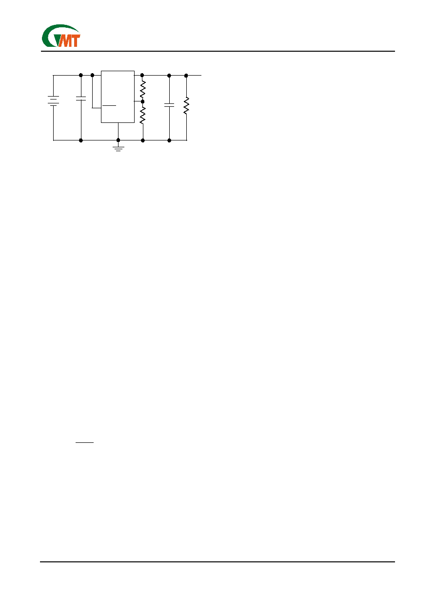
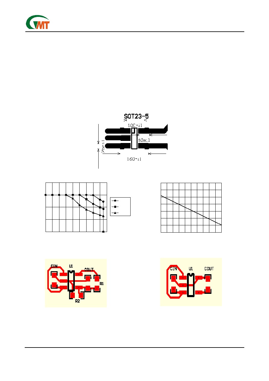
Layout Guide
An input capacitance of
1µF is required between the
G913 input pin and ground (the amount of the capaci-
tance may be increased without limit), This capacitor
must be located a distance of not more than 1cm from
the input and return to a clean analog ground.
Input capacitor can filter out the input voltage spike
caused by the surge current due to the inductive effect
of the package pin and the printed circuit board's
routing wire. Otherwise, the actual voltage at the IN
pin may exceed the absolute maximum rating.
The output capacitor also must be located a distance
of not more than 1cm from output to a clean analog
ground. Because it can filter out the output spike
caused by the surge current due to the inductive effect
of the package pin and the printed circuit board's
routing wire. Figure 6 is adjustable mode of G913 PCB
layout. Figure 7 is a PCB layout of G913 fixed mode.
Figure 4 Safe Operating Area
Safe Operating Area of G913 [Power Dissipation Limit]
0
50
100
150
200
0.0
0.5
1.0
1.5
2.0
2.5
3.0
3.5
4.0
4.5
Input-Output Voltage Differential V
IN
-V
OUT
(V)
Output Current (mA)
TA=25
TA=55
TA=85
Maximum Recommended Output Current
T
A
=25∞C,Still Air
1oz Copper on SOT-23-5 Package
Mounted on recommended mimimum footprint (R
JA=240
∞
C/W)
Maximum Power Dissipation of SOT-23-5
0
0.1
0.2
0.3
0.4
0.5
0.6
0.7
25
35
45
55
65
75
85
95
105
115
125
Amibent Temperature T
A
(∞C)
Power Dissipation (W)
Still Air
1oz Copper on SOT-23-5 Package
Mounted on recommend mimimum footprint (R
JA=240∞C/W
)
Note : V
IN(max)
<=5.5V
Figure 5 Power Dissipation vs. Temperature
Figure 4 Safe Operating Area
Figure 6. Adjustable Mode
Figure 7. Fixed Mode
*Distance between pin & capacitor must no more than 1cm
*Distance between pin & capacitor must no more than 1cm
Figure 3. Recommended Minimum Footprint

Ver 0.9 Preliminary
Jan 25, 2002
TEL: 886-3-5788833
http://www.gmt.com.tw
10
G913
Global Mixed-mode Technology Inc.
Package Information
Note:
1. Package body sizes exclude mold flash protrusions or gate burrs
2. Tolerance ±0.1000 mm (4mil) unless otherwise specified
3. Coplanarity: 0.1000mm
4.
Dimension L is measured in gage plane
DIMENSIONS IN MILLIMETERS
SYMBOLS
MIN
NOM MAX
A 1.00 1.10 1.30
A1 0.00 ----- 0.10
A2 0.70 0.80 0.90
b 0.35 0.40
0.50
C 0.10 0.15 0.25
D 2.70 2.90 3.10
E 1.40 1.60 1.80
e -----
1.90(TYP)
-----
e1 ----- 0.95 -----
H 2.60 2.80 3.00
L 0.37 ------ -----
1
1∫ 5∫ 9∫
Taping Specification
E
e
D
H
1
L
C
b
A2
A1
A
e1
E
e
D
H
1
L
C
b
A2
A1
A
e1
Feed Direction
SOT23-5 Package Orientation
Feed Direction
SOT23-5 Package Orientation