 | –≠–ª–µ–∫—Ç—Ä–æ–Ω–Ω—ã–π –∫–æ–º–ø–æ–Ω–µ–Ω—Ç: MFL2812S | –°–∫–∞—á–∞—Ç—å:  PDF PDF  ZIP ZIP |
MODELS
VDC O
UTPUT
1
Æ
Size (max): 3.005 x 1.505 x 0.400 inches (76.33 x 38.23 x 10.16 mm)
Case U
Weight:
100 grams maximum
Screening: Standard, ES, or 883 (Class H).
SINGLE
5
12
15
28
DUAL
±5
±12
±15
DESCRIPTION
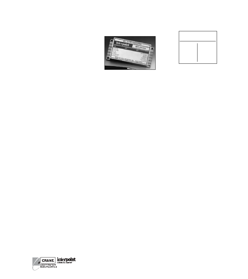
The MFL SeriesTM 28-volt DC/DC converters are rated up to 65
watts of output power over a ≠55∞C to +125∞C temperature range
with a 28 Vdc nominal input. On dual output models up to 70% of
the rated output power can be drawn from either the positive or
negative output. Current sharing allows the units to be paralleled for
total power of up to 148watts. The welded, hermetically sealed
package is only 3.005 x 1.505 x 0.400 inches, giving the series an
overall power density of up to 43 watts per cubic inch.
D
ESIGN
F
EATURES
The MFL Series converters are switching regulators that use a
quasi-square wave, single ended forward converter design with a
constant switching frequency of 600 kHz.
Isolation between input and output circuits is provided with a trans-
former in the forward path and a wide bandwidth magnetic coupling
in the feedback control loop. The MFL uses a unique dual loop feed-
back technique that controls output current with an inner feedback
loop and an output voltage with a cascaded voltage mode feedback
loop.
The additional secondary current mode feedback loop improves
transient response in a manner similar to primary current mode
control and allows for ease of paralleling, but without the cost and
complexity.
The cascaded constant frequency, pulse-width modulated
converters use a quasi-square wave single-ended forward design.
Tight load regulation is achieved through a wide-bandwidth
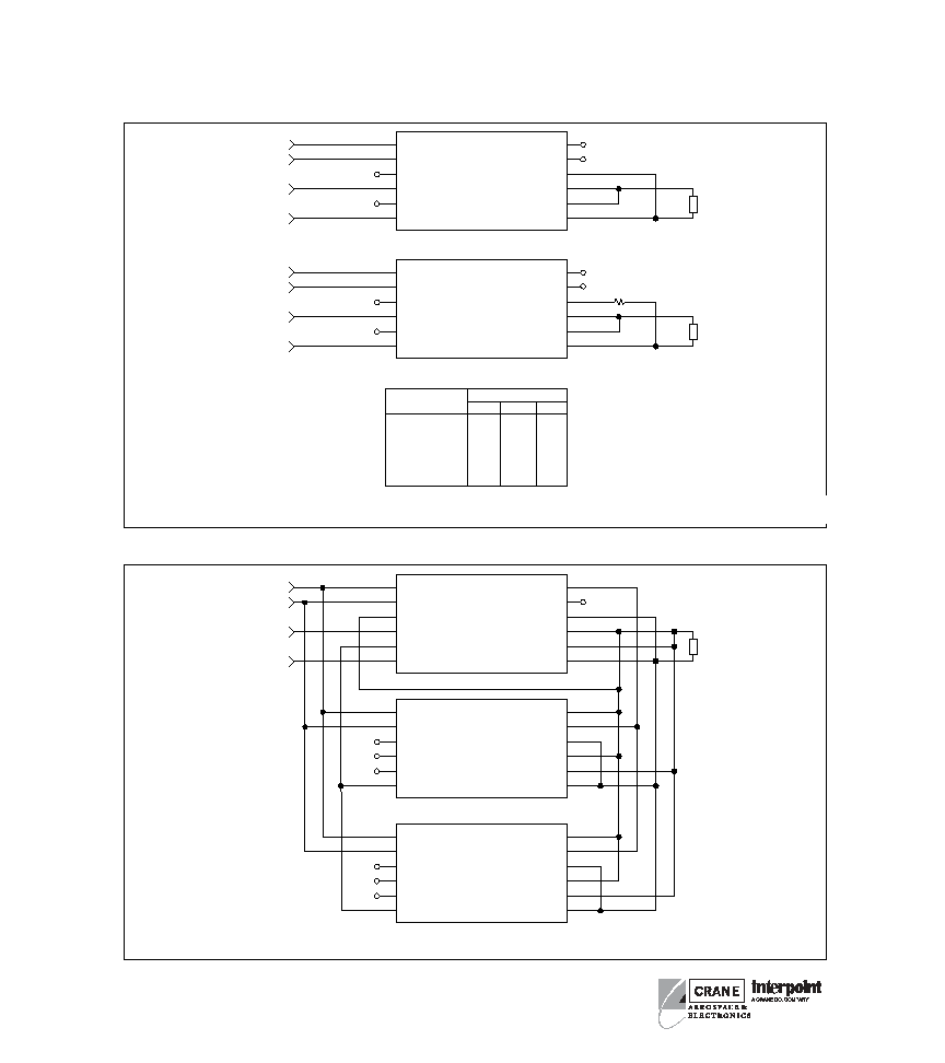
magnetic feedback circuit. The output on single MFL models can be
trimmed (see Figure 1 for voltage changes with different resistor
values).
I
NHIBIT
The MFL Series converters have two TTL compatible inhibit termi-
nals (INH1 and INH2) that can be used to disable power conversion,
resulting in a very low quiescent input current and no generation of
switching noise. An open collector TTL compatible low (<0.8 volts)
is required to inhibit the converter between INH1 (pin 4) and Input
Common (pin 2). An open collector TTL compatible low (<0.5 volts)
is required to inhibit the converter between INH2 (pin 12) and Output
Common (pin 8). The application of intermediate voltages to these
pins (1.5 to 10.5 volts) should be avoided.
C
URRENT AND
P
ARALLEL
O
PERATION
Multiple MFL converters may be used in parallel to drive a common
load (see Figure 2). In this mode of operation the load current is
shared by two or three MFL converters. In current sharing mode,
one MFL converter is designated as a master. The SLAVE pin (pin
11) of the master is left unconnected and the MSTR/INH2 pin (pin
12) of the master is connected to the SLAVE pin (pin 11) of the slave
units. The units designated as slaves have the MSTR/INH2 pin (pin
12) connected to the SNS RTN pin (pin 9). Figure 2 shows the
typical setup for two or three units in parallel. Note that synchro-
nizing the units together (though shown in the figure) is not required
for current sharing operation. A second slave unit may be placed in
parallel with a master and slave; this requires the TRI pin (pin 3) of
the master unit to be connected to the SNS RTN pin (pin 9).
When paralleled, 76% of the total combined power ratings of the
MFL converters are available at the load. Overload and short circuit
performance are not adversely affected during parallel operation.
DC/DC C
ONVERTERS
28 V
OLT
I
NPUT
MFL SERIES
65 WATT
F
EATURES
∑ ≠55∞ to +125∞C operation
∑ 16 to 40 VDC input
∑ Fully Isolated
∑ Magnetic feedback
∑ Fixed frequency, 600 kHz typical
∑ Topology ≠ Single Ended Forward
∑ 50 V for up to 50 ms transient protection
∑ Inhibit (input & output side)
∑ Sync function (in and out)
∑ Output trim on single output models
∑ Indefinite short circuit protection
∑ Remote sense on single output models
∑ Up to 87% efficiency / 43 W/in
3
∑ Parallelable up to 148 watts

TYPICAL CHARACTERISTICS
SYNC AND INHIBIT (INH1, INH2)
RECOMMENDED OPERATING CONDITIONS
ABSOLUTE MAXIMUM RATINGS
Input Voltage
∑ 16 to 40 VDC
Power Dissipation (Pd)
∑ 14 watts (16 watts MFL2805S, MFL2805D)
Output Power
∑ 50 to 65 watts depending on model
Lead Soldering Temperature (10 sec per lead)
∑ 300∞C
Storage Temperature Range (Case)
∑ ≠65∞C to +150∞C
2
MFL SERIES
65 WATT
DC/DC C
ONVERTERS
Æ
Output Voltage Temperature Coefficient
∑ 100 ppm/∞C typical
Input to Output Capacitance
∑ 150 pF, typical
Isolation
∑ 100 megohm minimum at 500 V
Audio Rejection
∑ 50 dB typical
Conversion Frequency
∑ Free run mode 600 kHz typical
550 kHz. min, 650 kHz max
∑ External sync range 525 to 675 kHz
Inhibit Pin Voltage (unit enabled)
∑ INH1 = 9 to12 V, INH2 = 6 to 9 V
Input Voltage Range
∑ 16 to 40 VDC continuous
∑ 50 V for 120 msec transient
Case Operating Temperature (Tc)
∑ ≠55∞C to +125∞C full power
∑ ≠55∞C to +135∞C absolute
Derate Output Power/Current
∑ Linearly from 100% at 125∞C to 0% at 135∞C
Electrical Characteristics: ≠55∞C to +125∞ C
1
Tc, 28 VDC Vin, 100% load, free run, unless otherwise specified.
Sync In (525 to 675 kHz)
∑ Duty cycle 40% min, 60% max
∑ Logic low 0.8 V max
∑ Logic high 4.5 V min, 9 V max
∑ Referenced to input common
∑ If not used, connect to input common
Sync Out
∑ Referenced to input common
Inhibit (INH1, INH2) TTL Open Collector
∑ Logic low (output disabled)
INH1 referenced to input common
Logic low 0.8 V max
Inhibit pin current 10 mA max
INH2 referenced to output common
Logic low 0.5 V max
Inhibit pin current 5 mA max
∑ Logic high (output enabled)
Open collector
Notes
1. MFL2828S specifiications are at 25∞Tc, contact your Interpoint repre-
sentative for more information.
2. Unit will shut down above approximately 45V but will be undamaged and
will restart when voltage drops into normal range.
3. Indefinite short circuit protection not guaranteed above 125∞C case.
4. Recovery time is measured from application of the transient to point at
which Vout is within 1% of final value.
5. Transition time
10 µs.
SINGLE OUTPUT MODELS
MFL2805S
MFL2812S
MFL2815S
MFL2828S
1
PARAMETER
CONDITION
MIN TYP MAX
MIN
TYP MAX
MIN
TYP MAX
MIN
TYP MAX
1
UNITS
OUTPUT VOLTAGE
Tc = 25∞C
4.95
5.00
5.05
11.88 12.00 12.12
14.85 15.00 15.15
27.72 28.00 28.28
VDC
OUTPUT CURRENT
V
IN
= 16 TO 40 VDC
0
--
10
0
--
5
0
--
4.33
0
--
2.32
A
OUTPUT POWER
V
IN
= 16 TO 40 VDC
0
--
50
0
--
60
0
--
65
0
--
65
W
OUTPUT RIPPLE
Tc = 25∞C
--
15
35
--
30
75
--
30
85
--
100
200
VOLTAGE 10 k - 2 MHz
Tc = ≠55∞C to +125∞C
--
30
50
--
45
100
--
45
110
--
--
--
mV p-p
LINE REGULATION
V
IN
= 16 to 40 VDC
--
0
20
--
0
20
--
0
20
--
20
60
mV
LOAD REGULATION
NO LOAD TO FULL
--
0
20
--
0
20
--
0
20
--
20
75
mV
INPUT VOLTAGE
CONTINUOUS
16
28
40
16
28
40
16
28
40
16
28
40
VDC
NO LOAD TO FULL
TRANSIENT
2
50 ms
--
--
50
--
--
50
--
--
50
--
--
50
V
INPUT CURRENT
NO LOAD
--
70
120
--
50
80
--
50
80
--
60
100
mA
FULL LOAD
--
--
2.5
--
--
2.8
--
--
3.0
--
--
2.8
A
INHIBITED - INH1
--
9
14
--
9
14
--
9
14
--
9
14
mA
INHIBITED - INH2
--
35
70
--
35
70
--
35
70
--
35
70
INPUT RIPPLE
CURRENT
10 kHz - 10 MHz
--
15
50
--
15
50
--
15
50
--
20
50
mA pp
EFFICIENCY
Tc = 25∞C
77
80
--
83
86
--
84
87
--
83
86
--
%
LOAD FAULT
3
POWER DISSIPATION
SHORT CIRCUIT
Tc = 25∞C
--
12.5
16
--
10
14
--
10
14
--
7
14
A
RECOVERY
--
1.5
4
--
1.5
4
--
1.5
4
--
1.0
4
ms
STEP LOAD RESP.
50% ≠ 100% ≠ 50%
TRANSIENT
--
250
350
--
450
600
--
500
600
--
800
1400
mV pk
RECOVERY
4
--
1.5
3.0
--
1.5
3.0
--
1.5
3.0
--
1.5
3.0
ms
STEP LINE RESP.
16 ≠ 40 ≠ 16 VDC
TRANSIENT
5
--
250
300
--
250
400
--
250
400
--
250
800
mV pk
RECOVERY
4
--
200
300
--
200
300
--
200
300
--
200
400
µs
START-UP
DELAY
--
3.5
6
--
3.5
6
--
3.5
6
--
3.5
6
ms
OVERSHOOT
--
0
25
--
0
50
--
0
50
--
0
100
mV pk
PINS NOT USED
TR1, Master, and Slave
If not used, leave unconnected

3
MFL SERIES
65 WATT
DC/DC C
ONVERTERS
Æ
Electrical Characteristics: ≠55∞C to +125∞C Tc, 28 VDC Vin, 100% load, free run, unless otherwise specified.
DUAL OUTPUT MODELS
MFL2805D
MFL2812D
MFL2815D
PARAMETER
CONDITIONS
MIN TYP
MAX
MIN
TYP
MAX
MIN
TYP
MAX
UNITS
OUTPUT VOLTAGE
Tc = 25∞C
+V
OUT
4.95
5.00
5.05
11.88 12.00
12.12 14.85 15.00
15.15
VDC
≠V
OUT
4.92
5.00
5.08
11.82 12.00
12.18
14.77 15.00
15.23
OUTPUT CURRENT
1
EACH OUTPUT
0
--
7
0
--
3.5
0
--
3.03
A
V
IN
= 16 TO 40 VDC
TOTAL OUTPUT
0
--
10
0
--
5
0
--
4.34
OUTPUT POWER
V
IN
= 16 TO 40 VDC
0
--
50
0
--
60
0
--
65
W
OUTPUT RIPPLE
VOLTAGE +/≠ V
OUT
10 kHz - 2 MHz
--
50
100
--
50
120
--
50
150
mV p-p
LINE REGULATION
+V
OUT
--
0
50
--
0
50
--
0
50
mV
V
IN
= 16 TO 40 VDC
≠V
OUT
--
25
100
--
25
100
--
25
100
LOAD REGULATION
+V
OUT
--
0
50
--
10
100
--
10
100
mV
NO LOAD TO FULL
≠V
OUT
--
25
100
--
50
120
--
50
150
CROSS REGULATION
SEE NOTE 2
--
5
8
--
2
4
--
2
4
%
Tc = 25∞C
SEE NOTE 3
--
3
6
--
2
4
--
2
4
INPUT VOLTAGE
CONTINUOUS
16
28
40
16
28
40
16
28
40
VDC
NO LOAD TO FULL
TRANSIENT
4
50 ms.
0
--
50
0
--
50
0
--
50
V
INPUT CURRENT
NO LOAD
--
50
120
--
50
100
--
50
100
mA
Tc = 25∞C
FULL LOAD
--
--
--
--
2.80
--
--
3.00
A
INHIBITED - INH1
--
9
14
--
9
14
--
9
14
mA
INHIBITED - INH2
--
35
70
--
35
70
--
35
70
INPUT RIPPLE
CURRENT
10 kHz - 10 MHz
--
15
50
--
15
50
--
15
50
mA p-p
EFFICIENCY 25∞C Tc
BALANCED LOAD
77
80
--
83
86
--
84
87
--
%
LOAD FAULT
5
POWER DISSIPATION
Tc = 25∞C
SHORT CIRCUIT
--
12.5
16
--
10
14
--
10
14
W
RECOVERY
--
1.5
4.0
--
1.5
4.0
--
1.5
4.0
ms
STEP LOAD
50 %≠100%≠ 50% LOAD
RESPONSE ± V
OUT
TRANSIENT
--
250
350
--
450
600
--
500
600
mV pk
RECOVERY
6
--
1.5
3.0
--
1.5
3.0
--
1.5
3.0
ms
STEP LINE
16 ≠ 40 ≠ 16 V
IN
RESPONSE ± V
OUT
TRANSIENT
7
--
250
300
--
250
400
--
250
400
mV pk
RECOVERY
6
--
200
300
--
200
300
--
200
300
µs
START≠UP
DELAY
--
3.5
6
--
3.5
6
--
3.5
6
ms
OVERSHOOT
--
0
25
--
0
50
--
0
50
mV p
Notes
1. Up to 70% of the total output power is available from either output providing
the opposite output is simultaneously carrying 30% of the total power.
2. Effect on the negative output under the following conditions:
+P
out
30% to 70%; ≠P
out
70% to 30%
3. Effect on the negative output under the following conditions:
+P
out
50%; ≠P
out
10% to 50%
4. Unit will shut down above approximately 45V but will be undamaged and will
restart when voltage drops into normal range.
5. Indefinite short circuit protection not guaranteed above 125∞C case.
6. Recovery time is measured from application of the transient to point at which
Vout is within 1% of final value.
7. Transition time
10 µs.
4
MFL SERIES
65 WATT
DC/DC C
ONVERTERS
Æ
SINGLE OUTPUT MODELS CONNECTION DIAGRAMS - SENSE AND PARALLEL
RL
1
2
3
4
5
6
REMOTE SENSE CONNECTION
12
11
10
9
8
7
≠
+
28V
≠
+
Inhibit
Sync In
RL
1
2
3
4
5
6
OUTPUT VOLTAGE ADJUST CONNECTION
12
11
10
9
8
7
≠
+
28V
≠
+
Inhibit
Sync In
0.1
0.2
0.3
0.4
0.5
70
140
210
280
350
25
50
75
100
125
20
40
60
80
100
RA (OHMS)
5≠V
12≠V
15≠V
VOUT INCREASE
(VOLT)
RA
Positive Input
Input Common
TR1
INH1
Sync Out
Sync In
MSTR/INH2
Slave
Pos. Sense
Sense Return
Output Common
Positive Output
Positive Input
Input Common
TR1
INH1
Sync Out
Sync In
MSTR/INH2
Slave
Pos. Sense
Sense Return
Output Common
Positive Output
RL
1
Positive Input
Input Common
TR1
INH1
Sync Out
Sync In
2
3
4
5
6
1
2
3
4
5
6
1
2
3
4
5
6
CONNECT ONLY WHEN 2 SLAVES ARE USED
12
11
10
9
8
7
12
11
10
9
8
7
12
11
10
9
8
7
≠
+
MSTR/INH2
Slave
Pos. Sense
Sense Return
Output Common
Positive Output
MASTER
SLAVE 1
SLAVE 2
28V
≠
+
Inhibit
Sync In
Positive Input
Input Common
TR1
INH1
Sync Out
Sync In
MSTR/INH2
Slave
Pos. Sense
Sense Return
Output Common
Positive Output
Positive Input
Input Common
TR1
INH1
Sync Out
Sync In
MSTR/INH2
Slave
Pos. Sense
Sense Return
Output Common
Positive Output
F
IGURE
1: S
ENSE
C
ONNECTIONS AND
T
RIM
T
ABLE
F
IGURE
2: P
ARALLEL
C
ONNECTIONS
PIN OUT
SMD NUMBERS
MFL 28 05 S / ES
Base Model
Input Voltage
Output Voltage
Screening
Number of Outputs
(S = single, D = dual)
(Standard screening has no designator
in this position.)
Angled corner indicates pin one.
1
2
3
4
5
6
12
11
10
9
8
7
TOP VIEW
MFL
(Pin side, marked side)
5
MFL SERIES
65 WATT
DC/DC C
ONVERTERS
Æ
MODEL NUMBERING KEY
Pin
Single Output
MFL2828S
Dual Output
1
Positive Input
Positive Input
Positive Input
2
Input Common
Input Common
Input Common
3
Triple (TRI)
Triple (TRI)
Triple (TRI)
4
Inhibit 1 (INH1)
Inhibit 1 (INH1)
Inhibit 1 (INH1)
5
Sync Out
Sync Out
Sync Out
6
Sync In
Sync In
Sync In
7
Positive Output
Positive Output
Positive Output
8
Output Common
No connection
Output Common
9
Sense Return
Output Common
Negative Output
10
Positive Sense
No connection
No connection
11
Slave
Slave
Slave
12
Master/ Inhibit 2
Master/ Inhibit 2
Master / Inhibit 2
Pin 6 should be connected to input common if
external sync (Sync In) is not used.
Sense pins must be connected to their respective
outputs if not used.
S
TANDARD
M
ICROCIRCUIT
D
RAWING
(SMD)
5962-9316301HXC
5962-9316201HXC
5962-9316101HXC
IN PROCESS
5962-9319101HXC
5962-9319201HXC
5962-9319301HXC
MFL S
ERIES
S
IMILAR
P
ART
MFL2805S/883
MFL2812S/883
MFL2815S/883
MFL2828S/883
MFL2805D/883
MFL2812D/883
MFL2815D/883
For exact specifications for an SMD product, refer to the
SMD drawing. See Section A3, SMDs, for more information.
Typical Performance Curves: 25∞C Tc , 28 VDC Vin, 100% load, free run, unless otherwise specified.
Output (Watts)
MFL2805S & MFL2805D Efficiency
Efficiency (%)
60
90
85
80
75
70
10
20
30
40
50
28V
40V
65
16V
F
IGURE
4
Output Power (Watts)
MFL2812S & MFL2812D Efficiency
Efficiency (%)
60
90
85
80
75
70
10
20
30
40
50
60
40V
16V
28V
65
F
IGURE
5
F
IGURE
6
60
90
85
80
75
70
10
20
30
40
50
65
60
65
16V
Output Power (Watts)
MFL2815S & MFL2815D Efficiency
Efficiency (%)
40V
28V
See Section B8, case U1, for dimensions.
F
IGURE
3: P
IN
O
UT