 | –≠–ª–µ–∫—Ç—Ä–æ–Ω–Ω—ã–π –∫–æ–º–ø–æ–Ω–µ–Ω—Ç: MFW | –°–∫–∞—á–∞—Ç—å:  PDF PDF  ZIP ZIP |

B4-3
MFW SERIES
70 WATTS
MODELS
VDC O
UTPUT
SINGLE
5
12
15
DUAL
±12
±15
TRIPLE
+5 & ±12
+5 & ±15
DC/DC C
ONVERTERS
28 V
OLT
I
NPUT
Size (max.): 3.20 x 2.46 x 0.595 inches (81.3 x 62.5 x 15.11 mm)
See Section B8, case L, for dimensions.
Weight:
140 grams typical
Screening: Standard or ES.See Section C2 for screening
options, see Section A5 for ordering information.
DESCRIPTION
The MFW SeriesTM of DC/DC converters offers up to 70 watts of
power from single, dual, or triple outputs in one package. Using
hybrid thick film technology a power density of over 20 watts per
cubic inch is achieved. These devices are packaged in hermetically
sealed cold rolled steel enclosures with a tin plate finish making
them ideal for use in military, aerospace, or other high reliability
applications. Unscreened models are guaranteed to pass a gross
leak test (maximum leak rate of 0.001 atm-cc/sec). Environmentally
screened units (designated by the /ES suffix) are hermetically solder
sealed. See Section C2 for screening specifications.
D
ESIGN
M
ETHODOLOGY
The MFW Series converters utilize a quasi-square wave forward
converter design with a nominal switching frequency of 245 kHz.
Isolation between input and output is provided with a transformer in
the forward power loop and a wideband, temperature insensitive
optical link in the feedback control loop. Output regulation is accom-
plished with constant frequency pulse width modulation. In addition,
the load regulation of the single output models is further enhanced
through the use of remote output voltage sense pins to overcome
the adverse effects of line resistance voltage drops. Short circuit
protection is provided by detecting peak primary switching current
on a cycle by cycle basis and limiting it to approximately 130% of the
full load input current. This method results in quick and positive
current limiting under short circuit conditions.
L
OW
N
OISE
The MFW Series converters offer low noise on both the input and
output lines. A two section, four pole LC input filter is included to
provide very low reflected line ripple current. Adherence to MIL-
STD-461C (CE03) is possible with the addition of the FMB-461 filter.
Output ripple is maintained at less than 50 mV p-p for single and
dual output models and 85 mV for triple output models.
W
IDE
V
OLTAGE
R
ANGE
All models of the MFW Series are designed to provide full power
operation over an input voltage range of 19 to 40 VDC. Operation
below an input of 19 volts, including operation in MIL-STD-704E
emergency power conditions, is possible with derated output power.
Please refer to the derating information and the low voltage drop-out
graphs (Figures 10 and 11) on the following pages.
W
IDE
T
EMPERATURE
R
ANGE
Full load operation of any of the MFW Series converters is available
at case temperatures of ≠55∞C to + 85∞C. Operation up to +125∞C
is possible with derated output power. The MFW Series converters
are provided in a flange mount case designed to facilitate the
removal of internally generated heat. Because of this, heat sinking
requirements are minimal. Sustained full power operation does
however require that an efficient heat sink be attached to the base-
plate. Please refer to the heat sink requirements section for more
information.
I
NHIBIT
/S
YNC
F
EATURE
Standard on all models of the MFW Series is a dual mode
inhibit/sync pin. This pin serves as both an output inhibit and as a
synchronization input. In the inhibit mode an open collector TTL
compatible low (<0.8 V) will disable internal switching thereby
inhibiting the unit's output. Inhibiting in this manner results in an
extremely low quiescent current. Since a pull-up resistor is included
internally, this pin may be left open should the inhibit function not be
desired.
In a digital system it is often desirable to synchronize the input or
output ripple with the system clock. For this reason each model of
the MFW Series was designed to synchronize with a system clock
applied to the inhibit/sync pin. Please refer to the technical data
section for timing details for the external sync feature.
F
EATURES
∑ ≠55∞C to + 85∞C operation
∑ 19 to 40 VDC input
∑ Fully Isolated
∑ Optocoupler feedback
∑ Fixed frequency, 245 kHz typical
∑ Topology ≠ Push-Pull Forward
∑ 50 V for up to 50 ms transient protection
∑ Inhibit/sync function
∑ Indefinite short circuit protection
∑ Remote sense on single models
∑ Up to 84% efficiency

RECOMMENDED OPERATING CONDITIONS
ABSOLUTE MAXIMUM RATINGS
TYPICAL CHARACTERISTICS
B4-4
MFW SERIES
70 WATT
DC/DC C
ONVERTERS
SINGLE OUTPUTS
MFW2805S
MFW2812S
MFW2815S
PARAMETER
CONDITION
MIN
TYP
MAX
MIN
TYP MAX
MIN.
TYP
MAX
UNITS
OUTPUT
FULL LOAD
4.95
5.00
5.05
11.88 12.00 12.12
14.85 15.00 15.15
VDC
VOLTAGE
OUTPUT
V
IN
= 19 TO 40
--
--
12.00
--
--
5.83
--
--
4.67
A
CURRENT
OUTPUT
Tc = ≠55∞C TO +85∞C
--
--
60
--
--
70
--
--
70
W
POWER
OUTPUT
FULL LOAD BW
2 MHz
--
30
50
--
30
50
--
30
50
mV p-p
RIPPLE
LINE
V
IN
= 19 TO 40
--
10
20
--
10
20
--
10
20
mV
REGULATION
LOAD
NO LOAD TO FULL
--
10
20
--
10
25
--
10
25
mV
REGULATION
INPUT
VOLTAGE
19
28
40
19
28
40
19
28
40
VDC
INPUT
NO LOAD
--
75
90
--
70
90
--
70
90
mA
CURRENT
INHIBITED
--
30
35
--
30
35
--
30
35
INPUT REFL.
FULL LOAD
--
10
25
--
10
25
--
10
25
mA p-p
RIPPLE
BW
10 MHz
EFFICIENCY
78
80
--
81
83
--
81
83
--
%
STARTUP
WITH LOW
--
5
10
--
8
10
--
8
10
ms
DELAY
IMPEDANCE SOURCE
Output Power
∑ 60 to 70 watts depending on model
Lead Soldering Temperature (10 sec per lead)
∑ 300∞C
Storage Temperature Range (Case)
∑ ≠55∞C to +125∞C
Output Voltage Temperature Coefficient
∑ 150 ppm/∞C, typical
Input to Output Capacitance
∑ 160 pF, typical
Isolation
∑ 100 megohm minimum at 500 V
Conversion Frequency
∑ Free run mode 245 kHz, typical
Inhibit Pin Voltage (unit enabled)
∑ 4.5 to 5.5 V
Electrical Characteristics: 25∞C Tc, 28 VDC Vin, 100% load, free run, unless otherwise specified.
Input Voltage Range
∑ 19 to 40 VDC continuous (see Derating)
Case Operating Temperature (Tc)
∑ ≠55∞C to +85∞C full power
SYNC AND INHIBIT
DERATING OUTPUT POWER/CURRENT AND INPUT VOLTAGE
Sync In (245 to 370 kHz.)
∑ Duty cycle 70% min, 98% max
∑ Logic low 0.8 V max
∑ Logic high 4.5 V min
∑ Referenced to input common
∑ If sync is not used, leave unconnected
Inhibit TTL Open Collector
∑ Logic low (output disabled)
Inhibit pin current 1 mA max
∑ Referenced to input common
∑ Logic high (output enabled)
V =
4.5 V
Temperatures are referenced to the temperature at the converter's baseplate
∑ Linearly derate output power/current from 100% at 85∞C to 0% at 125∞C.
∑ Above 105∞C linearly derate steady state input voltage to 33 volts at 125∞C.
∑ Indefinite short circuit protection is not guaranteed above 85∞C case.
∑ Operation below an input voltage of 19 volts, including operation in MIL-
STD-704E emergency power conditions, is possible with derated output
power. See Figures 10 and 11.

B4-5
MFW SERIES
70 WATT
DC/DC C
ONVERTERS
DUAL AND TRIPLE OUTPUTS
MFW2812D
MFW2815D
MFW28512T
MFW28515T
PARAMETER
CONDITION
MIN
TYP
MAX
MIN
TYP
MAX
MIN
TYP
MAX
MIN
TYP
MAX
UNITS
OUTPUT
FULL
MAIN
--
--
--
--
--
--
4.95
5.05
5.10
4.90
4.95
5.05
VOLTAGE
LOAD
DUAL
±11.88 ±12.00 ±12.12
±14.85 ±15.00 ±15.15 ±11.65
±11.80 ±12.05 ±15.05 ±15.30 ±15.55
VDC
OUTPUT
V
IN
=
MAIN
--
--
--
--
--
--
--
4.0
10.0
--
4.0
10.0
A
CURRENT
1, 2
19 TO 40
DUAL
--
2.92
5.5
--
2.33
4.4
--
1.67
4.2
--
1.33
3.33
OUTPUT
MAIN
--
--
--
--
--
--
--
20
50
--
20
50
POWER
1, 2
±DUAL
--
35
66.5
--
35
66.5
--
20
50
--
20
50
W
TOTAL
--
--
70
--
--
70
--
--
60
--
--
60
OUTPUT
FULL LOAD
MAIN
--
--
--
--
--
--
--
50
85
--
50
85
mV p-p
RIPPLE
BW
2 MHz
DUAL
--
30
50
--
30
50
--
50
85
--
50
85
LINE
V
IN
=
MAIN
--
--
--
--
--
--
--
2
20
--
2
20
mV
REGULATION 19 TO 40
DUAL
--
10
25
--
10
25
--
100
200
--
100
200
LOAD
3
NO LOAD
MAIN
--
--
--
--
--
--
--
5
20
--
5
20
mV
REGULATION TO FULL
DUAL
--
25
50
--
25
50
--
480
600
--
300
450
CROSS
4
DUAL
REGULATION +PO = 3 W TO 35 W
≠PO = 35 W
--
1.5
3.0
--
1.5
3.0
--
--
--
--
--
--
+PO = 20 W TO 50 W
%
≠PO = 50 W TO 20 W
--
2.0
4.0
--
2.0
3.5
--
--
--
--
--
--
CROSS
5
MAIN +PO = 33 W
REGULATION DUAL
+PO = 3 W TO 27 W
--
--
--
--
--
--
--
2.3
6.0
--
2.3
5.0
≠PO = 27 W TO 3 W
MAIN
%
+PO = 3 W TO 30 W
DUAL ±PO = 15 W
--
--
--
--
--
--
--
5.4
9.0
--
5.0
7.0
INPUT
VOLTAGE
19
28
40
19
28
40
19
28
40
19
28
40
VDC
INPUT
NO LOAD
--
75
90
--
75
90
--
60
110
--
60
110
mA
CURRENT
INHIBITED
--
30
35
--
30
35
--
30
35
--
30
35
INPUT REFL.
FULL LOAD
--
15
40
--
15
40
--
15
40
--
15
40
mA p-p
RIPPLE
BW
10 MHz
EFFICIENCY
80
83
--
80
83
--
80
84
--
80
84
--
%
STARTUP
--
15
25
--
15
25
--
6
10
--
6
10
ms
DELAY
Electrical Characteristics: 25∞C Tc, 28 VDC Vin, 100% load, free run, unless otherwise specified.
Notes
1. On dual output models the maximum combined output power is 70 watts.
A maximum of 95% (66.5 W) is available from any single output.
2. On triple output models the maximum combined output power is 60 watts.
A maximum of 50 watts is available from a single output.
3. Balanced loads.
4. Regulation effect on the negative dual output during the defined conditions.
5. Regulation effect on both dual outputs during the defined conditions.

B4-6
MFW SERIES
70 WATT
DC/DC C
ONVERTERS
C
ALCULATING
M
AXIMUM
A
MBIENT
T
EMPERATURE
The MFW Series of DC/DC converters has an upper operating
temperature of + 85∞C at the baseplate of the case. The degree of
heat sinking required to remain within this limit may be determined
from Figure 1 which shows the maximum allowed internal power
dissipation (P
DISS
vs. ambient temperature for various heat sink
thermal resistances. P
DISS
may be calculated as:
P
DISS
= P
OUT
/ efficiency ≠ P
OUT
The efficiency for all combinations of P
OUT
and V
IN
for the various
models may be obtained from the graphs on the preceding pages.
Example:
Converter = MFW2815D, T
AMB
= 70∞C,
V
IN
= 28 VDC, P
OUT
= 45 watts
Efficiency = 85% (From Figure 7)
P
DISS
= (45 / 85) ≠ 45 = 7.95 watts
From Figure 1 we can see that this situation will require thermal
resistance of approximately 4.5∞C / watt.
Conversely we may also find the maximum ambient temperature
which can be tolerated if we know the heat sink thermal resistance.
Example:
Converter = MFW2805S, V
IN
= 28 VDC, P
OUT
= 45 W.
Thermal Resistance = 3∞C / watt.
Efficiency = 83.5% (From Figure 3)
P
DISS
= (45 / 0.835) ≠ 45 = 8.89 watts.
From Figure 1 we can see that the maximum allowed ambient
temperature is approximately 75∞C.
H
EAT
S
INK
R
ECOMMENDATIONS
An MFW Series converter in still air (other than convective currents)
and with no conductive cooling paths other than through electrical
connections at the pins will exhibit a thermal resistance of approxi-
mately 4∞C / watt. In cases where this value proves to be too high it
is recommended that additional heat sinking be supplied. The
simplest method of accomplishing this is to firmly attach the
converter to a PCB thereby providing a conductive thermal path.
Secondly it is recommended that airflow be provided over the
converter. Although each situation requires a thorough thermal
analysis these two measures can reduce the thermal resistance to
as low as 2∞C / watt. If calculations indicate further heat sinking is
required it is recommended that additional thermal mass be
provided either under the base plate or on top of the converter's
mounting flanges or both.
THERMAL MANAGEMENT
Degrees Centigrade
Watts
20
∞
40
∞
60
∞
80
∞
100
∞
120
∞
140
∞
20
15
10
5
U=4
∞
C/W
U=3
∞
C/W
U=2
∞
C/W
U=0
∞
C/W
Internal Power Dissipation (max)
vs. Ambient Temperature
F
IGURE
1
PIN OUT
B4-7
MFW SERIES
70 WATT
DC/DC C
ONVERTERS
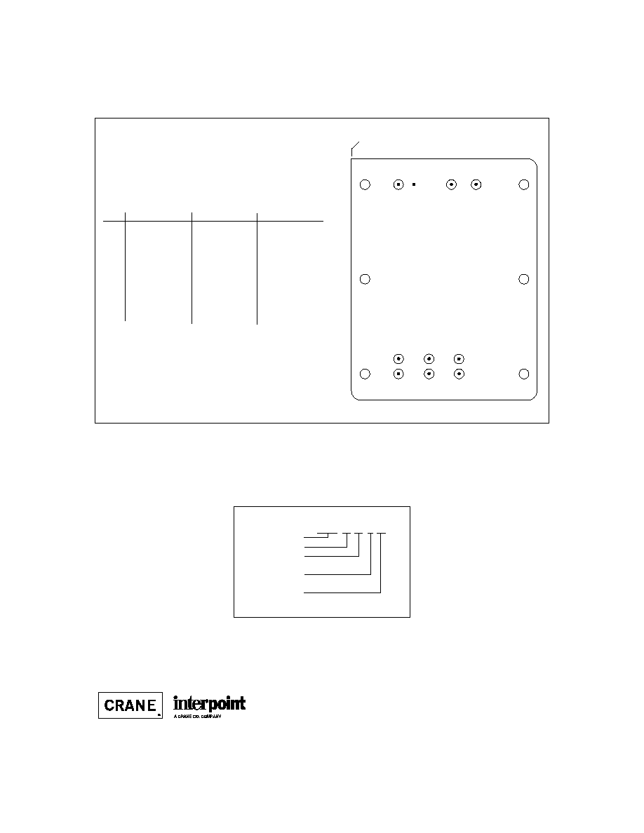
Squared corner indicates pin one.
BOTTOM VIEW
MFW
1
2
3
4
5
6
7
8
9
10
F
IGURE
2: P
IN
O
UT
MODEL NUMBERING KEY
MFW 28 512 T / ES
Base Model
Input Voltage
Output Voltage
Screening
Number of Outputs
(S = single, D = dual, T = triple)
(Main and Aux. Vout for triple models)
(Standard screening has no designator
in this position.)
Pin
Single Output
Dual Output
Triple Output
1
Positive Input
Positive Input
Positive Input
2
Case Ground
Case Ground
Case Ground
3
Input Common
Input Common
Input Common
4
Inhibit/Sync In
Inhibit/Sync In
Inhibit/Sync In
5
Negative Sense
Negative Output
Negative Aux. Output
6
Positive Sense
Positive Output
Positive Aux. Output
7, 8
Output Common
Output Common
Output Common
9, 10
Positive Output
No Connection
Main (+5) Output
See Section B8, case L, for dimensions.

B4-8
MFW SERIES
70 WATT
DC/DC C
ONVERTERS
Typical Performance Curves: 25∞C Tc , 28 VDC Vin, 100% load, free run, unless otherwise specified.
F
IGURE
6
F
IGURE
8
10
20
30
40
50
60
70
87
85
83
81
79
77
75
73
71
40 V
28 V
19 V
Efficiency (%)
Output Power (Watts)
MFW2812D Efficiency vs Line & Load
10
20
30
40
50
60
70
87
85
83
81
79
77
75
73
71
40 V
28 V
19 V
Efficiency (%)
Output Power (Watts)
MFW28512T Efficiency vs Line & Load
Efficiency (%)
10
20
30
40
50
60
70
86
85
84
83
82
81
80
79
78
40 V
28 V
20 V
Output Power (Watts)
MFW2805S Efficiency vs Line & Load
F
IGURE
3
10
20
30
40
50
60
70
89
88
87
86
85
84
83
82
81
40 V
28 V
19 V
Efficiency (%)
Output Power (Watts)
MFW2812S Efficiency vs Line & Load
F
IGURE
4
10
20
30
40
50
60
70
87
85
83
81
79
77
75
73
71
40 V
28 V
19 V
Efficiency (%)
Output Power (Watts)
MFW2815D Efficiency vs Line & Load
F
IGURE
7
F
IGURE
5
10
20
30
40
50
60
70
89
88
87
86
85
84
83
82
81
40 V
28 V
19 V
Efficiency (%)
Output Power (Watts)
MFW2815S Efficiency vs Line & Load
10
20
30
40
50
60
70
87
85
83
81
79
77
75
73
71
40 V
28 V
19 V
Efficiency (%)
Output Power (Watts)
MFW28515T Efficiency vs Line & Load
F
IGURE
9
Input Voltage (Volts)
15
10
20
30
40
50
60
70
16
17
18
283R5S
2815S
2812S
2805S
Output Power (Watts)
Low Line Dropout vs. Load (50 mV drop)
MFW Single Output Models
F
IGURE
10
F
IGURE
11
15
10
20
30
40
50
60
70
16
17
18
19
MFW2815D
MFW2812D
MFW28512T
MFW28515T
Input Voltage (Volts)
Output Power (Watts)
Low Line Dropout vs. Load (50 mV drop)
MFW Dual and Triple Output Models
20621-001-DTS Rev A
DQ# 1016
All technical information is believed to be accurate, but no responsibility is
assumed for errors or omissions. Interpoint reserves the right to make changes in
products or specifications without notice. MFW Series is a trademark of Interpoint.
Copyright © 1991- 1999 Interpoint. All rights reserved.

B8-31
CASE L
C
ASES
0.060 min
(1.52)
0.060 min
(1.52)
0.337 min
(8.56)
0.337 min
(8.56)
3.20 max (81.3)
2.46 max (62.5)
Materials
Header Cold Rolled Steel/Nickel/Tin
Cover
Cold Rolled Steel/Nickel/Tin
Pins
#52 alloy pins 1-4, and 9-10
#52 alloy with copper core pins 5-8
ceramic seal
Case dimensions in inches (mm)
Tolerance
±
0.005 (0.13) for three decimal places
±
0.01 (0.2) for two decimal places
unless otherwise specified
CAUTION
Heat from reflow or wave soldering may damage
the device. Solder pins individually with heat
application not exceeding 300
∞
C for 10 seconds
per pin.
Squared corner indicates pin one
CASE L
TOP VIEW
Cover Placement
and
Min/Max Dimensions
See Figure 50
for pin configuration
F
IGURE
49: C
ASE
L M
AXIMUM
D
IMENSIONS

B8-32
CASE L
C
ASES
Solder Seal
Solder Tip-off
2.850 (72.39)
0.550 (13.97)
1.600 (40.64)
0.350 (8.89)
0.000
0.00
0.000
0.180 (4.57)
0.040 +0.007/-0.000
(1.02 +0.18/-0.00)
0.595 max
(15.11)
0.250 +0.05/-0.00
(6.35 +1.3/-0.0)
0.625 (15.88)
0.825 (20.96)
1.025 (26.04)
1.325 (33.66)
1.425 (36.20)
1.625 (41.28)
2.280 (57.91)
.0.040 +0.005/-0.002
(1.02 +0.13/-0.05)
BOTTOM VIEW
1
2
3
4
5
6
7
8
9
10
Squared corner indicates pin one
MFW Series: Screening ≠ Standard or ES
HR700 Series: no screening options
CASE L
0.141 x 6
(3.58)
F
IGURE
50: C
ASE
L D
IMENSIONS

C2-12
QA SCREENING
85∞C PRODUCTS
TEST (85∞C Products excluding HR products)
STANDARD
/ES
PRE-CAP INSPECTION
Method 2017
yes
yes
TEMPERATURE CYCLE (10 times)
Method 1010, Cond. B, -55∞C to 125∞C
no
yes
CONSTANT ACCELERATION
Method 2001, 500 g
no
yes
BURN-IN
96 hours at 70∞C ambient (typical)
no
yes
FINAL ELECTRICAL TEST MIL-PRF-38534, Group A
Subgroups 1 and 4: +25∞C case
yes
yes
HERMETICITY TESTING
Fine Leak, Method 1014, Cond. A
no
yes
Gross Leak, Method 1014, Cond. C
no
yes
Gross Leak, Dip (1 x 10
-3
)
yes
no
FINAL VISUAL INSPECTION
Method 2009
yes
yes
Test methods are referenced to MIL-STD-883 as determined by MIL-PRF-38534.
MFW Series
MTW Series
MHE/MLP Series
MHL Series
MRH Series
MTO Series
MSR Series
DCH Series
FM/FMA/FMB EMI Filters
MSF EMI Filter
85∞C P
RODUCTS
Applies to the following products: