 | –≠–ª–µ–∫—Ç—Ä–æ–Ω–Ω—ã–π –∫–æ–º–ø–æ–Ω–µ–Ω—Ç: MGA2815D | –°–∫–∞—á–∞—Ç—å:  PDF PDF  ZIP ZIP |

MODELS
VDC O
UTPUT
B2-81
Size (max.): 1.110 x 1.110 x 0.250 inches (28.19 x 28.19 x 6.35 mm)
Shown with "Gull Wing" lead option, also available with straight
leads. See Section B8, case D, for dimensions and options.
Weight:
15 grams maximum.
Screening: Standard, ES, or 883 (Class H). See Section B9 for
screening options, see Section A5 for ordering information.
SINGLE
5
12
15
DUAL
±5
±12
±15
DESCRIPTION
The MGA SeriesTM of DC/DC converters delivers 5 watts of output
power from a wide input voltage range of 16 to 40 VDC with up to
74% efficiency. Output models of 5, 12, 15, ±5, ±12 and ±15 VDC
meet a variety of system needs. All units withstand transients of up
to 50 V for up to 50 milliseconds and operate over the full military
temperature range of -55∞C to +125∞C.
C
ONVERTER
D
ESIGN
The MGA converters incorporate flyback topology with a typical
constant switching frequency of 500 kHz. Isolation between input
and output circuits is provided with a transformer in the forward path
and a temperature compensated optical link in the feedback control
loop. The feed-forward compensation design delivers an audio
rejection of 50 dB, typical, with input ripple as low as 50 mA p-p and
output ripple as low as 100 mV p-p. Output filter examples in Figures
3 and 4 provide suggested solutions for systems where very low
output ripple is required.
Tightly coupled magnetics minimize cross regulation in the MGA
dual output models. Either output can provide up to 80% of the total
available output power, providing the opposite output is carrying at
least 20% of the total output power.
The converter's short circuit current protection restricts the output
current to approximately 115% of the full load output current.
I
NHIBIT
F
UNCTION
The MGA converter's inhibit terminal disables internal switching,
resulting in no output and very low quiescent input current. Applying
a TTL low voltage (0.8 V or less) to the inhibit terminal (pin 1)
disables the output. Leaving the inhibit terminal unconnected or
connecting the inhibit terminal to an open collector gate enables the
output. The inhibit terminal has an open circuit voltage of 9 to 11 V.
In the inhibit mode the inhibit pin will source a maximum of 4 mA.
See "Inhibit Interface," Figure 2.
MIL-STD-461
Use Interpoint's FMGA-461 EMI filter to pass the CE03 require-
ments of MIL-STD-461C.
S
URFACE
M
OUNT
P
ACKAGE
The MGA DC/DC converters can be surface mounted with pick-and-
place equipment or manually. It is recommended that the case be
attached with flexible epoxy adhesive or silicone which is thermally
conductive (>1 watt /meter/∞K).
Internal components are soldered with SN96 (melting temperature
221∞C) to prevent damage during reflow. Maximum reflow tempera-
ture for surface mounting the MGA converter is 220∞C for a
maximum of 30 seconds. SN60, 62, or 63 are the recommended
types of solder. Hand soldering should not exceed 300∞C for 10
seconds per pin.
The hermetically sealed metal cases are available in two different
lead configurations. See Section B8, cases D1 and D2.
DC/DC C
ONVERTERS
28 V
OLT
I
NPUT
MGA SERIES
5 WATT
F
EATURES
∑ ≠55∞ to +125∞C operation
∑ 16 to 40 VDC input
∑ Fully Isolated
∑ Optocoupler feedback
∑ Fixed frequency 550 kHz typical
∑ Topology ≠ Single Ended Flyback
∑ 50 V for up to 50 ms transient protection
∑ Inhibit function
∑ Indefinite short circuit protection
∑ Up to 74% efficiency

ABSOLUTE MAXIMUM RATINGS
TYPICAL CHARACTERISTICS
INHIBIT
RECOMMENDED OPERATING CONDITIONS
B2-82
MGA SERIES
5 WATT
DC/DC C
ONVERTERS
Output Voltage Temperature Coefficient
∑ 100 ppm/∞C typ, 150 ppm/C max
Current Limit
∑ 115% of full load typical
Isolation
∑ Input to output
∑ Any pin to case except case pins
∑ 100 megohm minimum at 500 V
Conversion Frequency
∑ 500 kHz typical
450 kHz. min, 600 kHz max
Inhibit Pin Voltage (unit enabled)
∑ 9 to 11 V
Input Voltage Range
∑ 16 to 40 VDC continuous
∑ 50 V for up to 50 msec transient
Case Operating Temperature (Tc)
∑ ≠55∞C to +125∞C full power
∑ ≠55∞C to +135∞C absolute
Derating Output Power/Current (Tc)
∑ Linearly from 100% at 125∞C to 0% at 135∞C
Electrical Characteristics: 25∞C Tc, 28 VDC Vin, 100% load, unless otherwise specified.
Inhibit: TTL Open Collector
∑ Logic low (output disabled)
Logic low voltage
0.8 V
∑ Referenced to input common
∑ Logic high (output enabled)
Open collector
Input Voltage
∑ 16 to 40 V
Output Power
∑ 5 watts
Lead Soldering Temperature
∑ Reflow 220∞C 30 sec. max
SN60, 62 or 63 recommended solder
∑ Hand solder 300∞C 10 sec. max. per lead
Storage Temperature Range (Case)
∑ ≠65∞C to +150∞C
SINGLE OUTPUT MODELS
MGA2805S
MGA2812S
MGA2815S
PARAMETER
CONDITIONS
MIN
TYP
MAX
MIN
TYP
MAX
MIN
TYP
MAX
UNITS
OUTPUT VOLTAGE
+V
OUT
4.95
5.0
5.05
11.88
12
12.12
14.85
15
15.15
VDC
OUTPUT CURRENT
V
IN
= 16 to 40 VDC
0
--
1000
0
--
417
0
--
333
mA
OUTPUT POWER
V
IN
= 16 to 40 VDC
--
--
5
--
--
5
--
--
5
W
OUTPUT RIPPLE
10 kHz - 2 MHz
--
250
450
--
100
500
--
100
600
mV p-p
LINE REGULATION
V
IN
= 16 to 40 VDC
--
10
50
--
10
50
--
10
50
mV
LOAD REGULATION
NO LOAD TO FULL
--
10
50
--
10
50
--
10
50
mV
INPUT VOLTAGE
CONTINUOUS
16
28
40
16
28
40
16
28
40
VDC
NO LOAD TO FULL
TRANSIENT 50 ms
--
--
50
--
--
50
--
--
50
V
INPUT CURRENT
NO LOAD
--
27
60
--
29
60
--
31
60
FULL LOAD
--
--
279
--
--
263
--
--
259
mA
INHIBITED
--
3
4
--
3
4
--
3
4
INPUT RIPPLE
Tc = 25∞C
--
50
200
--
50
200
--
50
200
mA p-p
10 kHz - 10 MHz
Tc = ≠55∞C to +125∞C
--
75
300
--
75
300
--
75
300
EFFICIENCY
64
69
--
68
74
--
69
74
--
%
LOAD FAULT
1
SHORT CIRCUIT
POWER DISS.
--
1.5
2.0
--
1.2
1.9
--
1.2
1.8
W
RECOVERY
--
10
75
--
10
30
--
10
30
ms
STEP LOAD
50% ≠ 100% ≠ 50% LOAD
RESPONSE
2
TRANSIENT
≠500
200
500
≠750
300
750
≠1000
400
1000
mV pk
RECOVERY
3
--
200
500
--
400
1000
--
400
1000
µs
STEP LINE
16 ≠ 40 ≠ 16 VDC
RESPONSE
4
TRANSIENT
≠500
100
500
≠800
200
800
≠500
100
500
mV pk
RECOVERY
3
--
.4
1.0
--
0.5
1.3
--
0.5
1.3
ms
START-UP
OVERSHOOT
0
0
200
0
0
500
0
0
500
mV pk
DELAY
0
10
75
0
10
30
0
10
30
ms
INHIBIT PIN
CURRENT
INHIBITED
--
2.5
4.0
--
2.5
4.0
--
2.5
4.0
mA
CAPACITANCE
INPUT TO OUTPUT
--
50
--
--
40
--
--
60
--
pF
CAPACITIVE LOAD
--
--
300
--
--
500
--
--
500
µF
Notes
1. Indefinite short circuit protection not guaranteed above 125∞C (case).
2. Load transient transition time is >10 µs.
3. Recovery time is measured from application of the transient to the point at
which Vout is within regulation.
4. Input step transition time is >10µs.

B2-83
MGA SERIES
5 WATT
DC/DC C
ONVERTERS
DUAL OUTPUT MODELS
MGA2805D
MGA2812D
MGA2815D
PARAMETER
CONDITIONS
MIN
TYP MAX
MIN
TYP
MAX
UNITS
OUTPUT VOLTAGE
+V
OUT
11.88
12
12.12
14.85
15
15.15
VDC
≠V
OUT
≠11.76 ≠12 ≠12.24
≠14.70 ≠15 ≠15.30
OUTPUT CURRENT
V
IN
= 16 to 40 VDC
0
±208 333
0
±167
267
mA
OUTPUT POWER
1
V
IN
= 16 to 40 VDC
--
--
5
--
--
5
W
OUTPUT RIPPLE
2
10 kHz - 2 MHz
--
120
300
--
120
300
mV p-p
LINE REGULATION
+V
OUT
--
10
50
--
10
50
mV
V
IN
= 16 to 40 VDC
≠V
OUT
--
40
180
--
40
180
LOAD REGULATION
+V
OUT
(BALANCED)
--
10
50
--
10
50
mV
NO LOAD TO FULL
≠V
OUT
(BALANCED)
--
50
200
--
50
200
CROSS REG.
3
EFFECT ON ≠V
OUT
--
8
15
--
7
15=
%
INPUT VOLTAGE
CONTINUOUS
16
28
40
16
28
40
VDC
NO LOAD TO FULL
TRANSIENT 50 ms
--
--
50
--
--
50
V
INPUT CURRENT
NO LOAD
--
33
63
--
38
63
FULL LOAD
--
--
267
--
--
263
mA
INHIBITED
--
3
4
--
3
4
INPUT RIPPLE
Tc = 25∞C
--
50
200
--
50
200
mA p-p
10 kHz - 10 MHz
Tc = ≠55∞C to +125∞C
--
75
300
--
75
300
EFFICIENCY
67
73
--
68
73
--
%
LOAD FAULT
4
SHORT CIRCUIT
POWER DISS.
--
1.3
1.7
--
1.3
1.6
W
RECOVERY
--
10
30
--
10
30
ms
STEP LOAD TRANSIENT
≠550
180
550
≠600
180
600
mV
pk
RESP O N S E
5, 6
RECOVERY
7
--
200
500
--
200
500
µs
STEP LINE
16 ≠ 40 ≠ 16 VDC
RESP O N S E
8
TRANSIENT
≠500
100
500
≠1500 200
1500
mV pk
RECOVERY
7
--
0.8
2.0
--
1.6
4.0
ms
START-UP
OVERSHOOT
0
200
500
0
200
500
mV pk
DELAY
0
10
30
0
10
30
ms
INHIBIT PIN
CURRENT
UNIT INHIBITED
--
2.5
4.0
--
2.5
4.0
mA
CAPACITANCE
INPUT TO OUTPUT
--
50
--
--
50
--
pF
CAPACITIVE LOAD
--
--
100
--
--
100
µF
Electrical Characteristics: 25∞C Tc, 28 VDC Vin, 100% load, unless otherwise specified.
Notes
1. Up to 4 watts, 80% of the total output power is available from either output
providing the opposite output is simultaneously carrying 20% of the total
output power. Each output must carry a minimum of 20% of the total output
power in order to maintain regulation on the negative output.
2. Applies to both +Vout and ≠Vout
3. Cross regulation is specified for the following percentages of total output
power: +PO = 20% and ≠PO = 80% to +PO =80% and ≠PO = 20%
4. Indefinite short circuit protection not guaranteed above 125∞C (case).
5. Load transient transition time is >10 µs.
6. Response of either output when the load for each output is simultaneously
transitioned from 25% to 50% to 25% of total output power (5 watts).
7. Recovery time is measured from application of the transient to the point at
which Vout is within regulation.
8. Input step transition time is >10µs.
A
VAILABLE
SOON
,
ASK YOUR
I
NTERPOINT REP
FOR INFORMA
-
TION
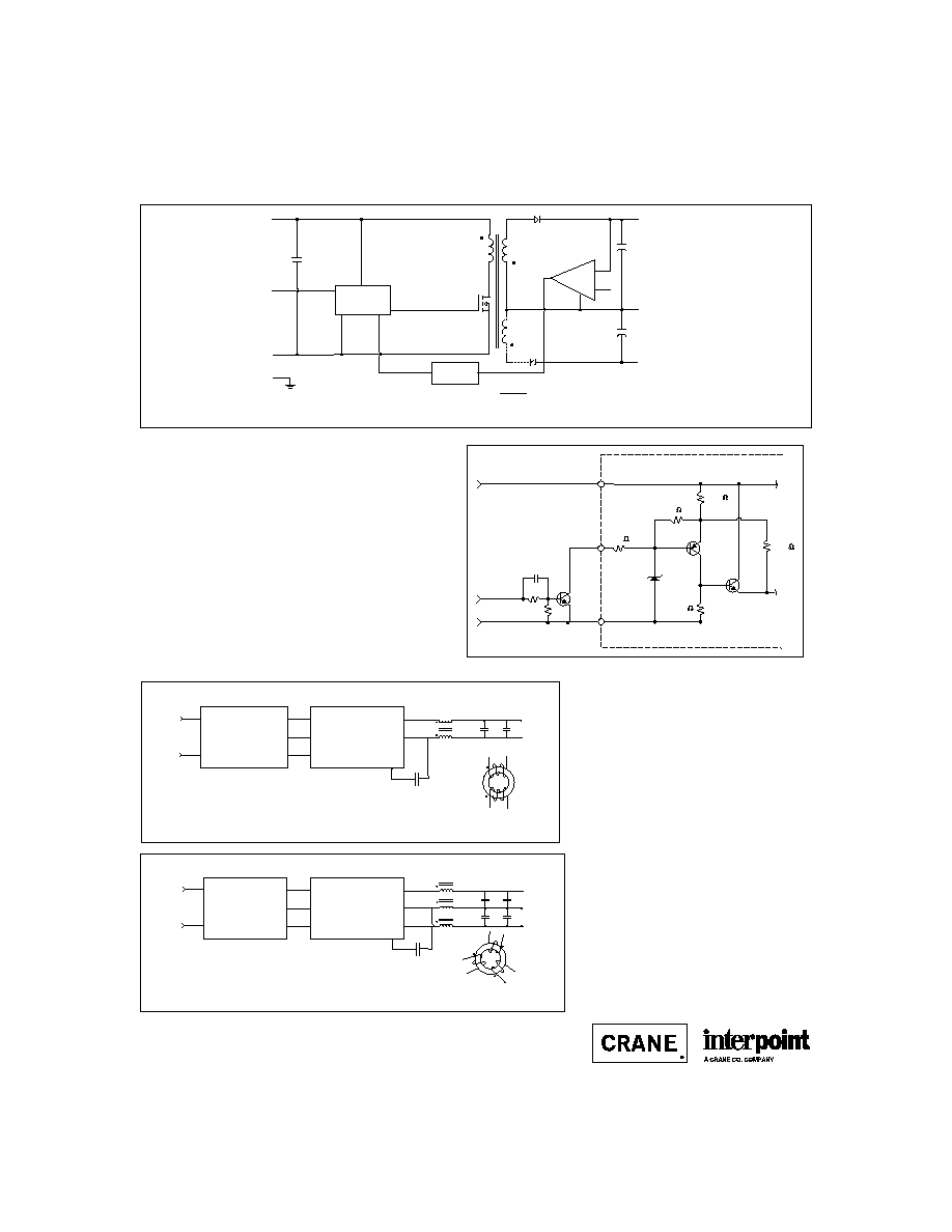
+
C2
T1
C1
Case
C3
MGA2815S
Input
Common
Positive
Input
Positive
Output
Output Common
To Load
Positive
Input
Input
Common
Positive
Output
Output
Common
From input
power source
EMI Filter
Case
T1
Negative
Output
Output
Common
Positive
Output
Input
Common
Case
Ground
Positive
Input
Inhibit
PWM
Control
Error
Amp
Isolated
Feedback
VR
= Dual Output
+
+
MGA SERIES
5 WATT
DC/DC C
ONVERTERS
B2-84
F
IGURE
1: B
LOCK
D
IAGRAM
DIAGRAMS AND CONNECTIONS
F
IGURE
3: L
OW
N
OISE
O
UTPUT
F
ILTER
MGA S
INGLE
O
UTPUT
M
ODEL
F
IGURE
4: L
OW
N
OISE
O
UTPUT
F
ILTER
MGA D
UAL
O
UTPUT
M
ODEL
The filter suggestions in Figures 3 and 4 will further
reduce the output ripple for systems requiring very low
output noise.
C1 = 0.27 µF ceramic capacitor, 500V
C2 = C4 = 6.8 µF tantalum capacitor
C3 = C5 = 0.27 µF ceramic capacitor
Single output: T1 = 15T #28 AWG winding on toroid,
m = 5000
Dual output: T2 = 10T #28 AWG winding on toroid,
m = 5000
F
IGURE
2: I
NHIBIT
I
NTERFACE
200 pF
3.9 K
10 K
Inhibit
Input
Common
10 k
12 k
5 k
400
50 k
2N3904
10V
MGA
Vcc
Positive
Input
+
C2
T1
C1
T2
C4
C3
C5
+
To Loads
Case
MGA2815D
Input
Common
Positive
Input
Positive
Output
Output Common
Positive
Input
Input
Common
Positive
Output
Output
Common
From input
power source
EMI Filter
Case
Negative
Output

SMD NUMBERS
PIN OUT
TOP VIEW
MGA
1
2
3
4
5
6
7
8
9
10
18
17
16
15
14
13
12
11
19
20
Differently colored glass bead around pin one or dimple in
header (bottom of case) indicates pin one.
Cover marking is oriented with pin one at the upper right corner.
B2-85
MGA SERIES
5 WATT
DC/DC C
ONVERTERS
MODEL NUMBERING KEY
MGA 28 12 S Z / ES
Base Model
Input Voltage
Output Voltage
Screening
Number of Outputs
(S = single, D = dual)
Gull Wing Lead Option
(Straight leaded case has no designator
in this position.)
(Standard screening has no designator
in this position.)
Pin
Single Output
Dual Output
1
Inhibit
Inhibit
2, 3
Positive Input
Positive Input
4
No connection
No connection
5, 6
Input Common
Input Common
7, 8
Case Ground
Case Ground
9, 10
No connection
No connection
11, 12 Positive Output
Positive Output
13
Positive Output
Output Common
14
Output Common
Output Common
15, 16 Output Common
Negative Output
17, 18 No connection
No connection
19, 20 Case Ground
Case Ground
Typical Performance Curves: 25∞C Tc , 28 VDC Vin, 100% load, unless otherwise specified.
F
IGURE
9
F
IGURE
11
OUTPUT POWER (Watts)
MGA2815D
EFFICIENCY vs LINE & LOAD
EFFICIENCY (%)
30
80
40V
70
60
50
40
1
2
3
4
5
6
16V
28V
MGA2815D
30
40
50
60
ATTENUATION (dB)
70
1
AUDIO REJECTION
10
0.1
FREQUENCY (kHz)
OUTPUT POWER (Watts)
MGA2805S
EFFICIENCY vs LINE & LOAD
EFFICIENCY (%)
30
80
40V
70
60
50
40
1
2
3
4
5
6
16V
28V
F
IGURE
6
OUTPUT POWER (Watts)
MGA2812S
EFFICIENCY vs LINE & LOAD
EFFICIENCY (%)
30
80
40V
70
60
50
40
1
2
3
4
5
6
16V
28V
F
IGURE
7
30
40
50
60
ATTENUATION (dB)
70
1
AUDIO REJECTION
10
0.1
FREQUENCY (kHz)
MGA2805S
F
IGURE
10
F
IGURE
8
OUTPUT POWER (Watts)
MGA2815S
EFFICIENCY vs LINE & LOAD
EFFICIENCY (%)
30
80
40V
70
60
50
40
1
2
3
4
5
6
16V
28V
F
IGURE
5: P
IN
O
UT
S
TANDARD
M
ICROCIRCUIT
D
RAWING
(SMD)
5962-9309201HXC
5962-9309301HXC
5962-9309401HXC
IN PROCESS
5962-9308901HXC
5962-9309001HXC
MGA S
ERIES
S
IMILAR
P
ART
MGA2805S/883
MGA2812S/883
MGA2815S/883
MGA2805D/883
MGA2812D/883
MGA2815D/883
Replace the "Y" with a "Z" in the SMD number to specify gull-wing leads.
For exact specifications for an SMD product, refer to the SMD drawing.
See Section A3, SMDs, for more information.
To meet specified performance, all pins must be
connected except "No Connection" pins.
See Section B8, case D for dimensions and gull-wing lead option.

B2-86
MGA SERIES
5 WATT
DC/DC C
ONVERTERS
Typical Performance Curves: 25∞C Tc , 28 VDC Vin, 100% load, unless otherwise specified.
F
IGURE
15
F
IGURE
17
1ms/div
TURN-ON INTO NO LOAD, MGA2805S
1V/div.
V
in
20V/div.
V
out
200
µ
s/div
+V
out
LOAD TRANSIENT RESPONSE
(10% 90%), MGA2815D
200mV/div.
10% to 90%
90% to 10%
≠P
out
=0.5W
100
µ
s/div
INPUT LINE TRANSIENT RESPONSE
(16V TO 40V), MGA2805S
20mV/div.
V
in
20V/div.
V
out
F
IGURE
12
100
µ
s/div
LOAD TRANSIENT RESPONSE
(10% 100%), MGA2805S
50mV/div.
10% to 100%
100% to 10%
F
IGURE
13
200
µ
s/div
INPUT LINE TRANSIENT RESPONSE
(16V TO 40V), MGA2815D
100mV/div.
V
in
20V/div.
+V
out
≠V
out
F
IGURE
16
F
IGURE
14
100
µ
s/div
LOAD TRANSIENT RESPONSE
(50% 100%) MGA2805S
50mV/div.
50% to 100%
100% to 50%
F
IGURE
21
OUTPUT LOAD (%)
MGA2815D/MGA2812D
CROSS REGULATION
COND. A: 50% LOAD +V; 10% to 50% ≠V
COND. B: 50% LOAD ≠V; 10% to 50% +V
≠V
out
VOLTAGE CHANGE (%)
≠5
0
5
10
20
30
40
50
≠4
≠3
≠2
≠1
1
2
3
4
2815D
2812D
2812D
COND B
COND A
100
µ
s/div
+V
out
LOAD TRANSIENT RESPONSE
(10% 50%), MGA2815D
100mV/div.
10% to 50%
50% to 10%
≠P
out
=2.5W
F
IGURE
18
500
µ
s/div
TURN-ON INTO NO LOAD, MGA2815D
5V/div.
V
in
20V/div.
+V
out
≠V
out
F
IGURE
19
F
IGURE
20
OUTPUT LOAD (+V
out
%/≠V
out
%)
MGA2815D/MGA2812D
CROSS REGULATION
(90≠10% LOAD on +V, 10-90% LOAD on ≠V)
≠V
out
VOLTAGE CHANGE (%)
≠10
0
10
90/10 70/30 50/50 30/70 10/90
≠8
≠6
≠4
≠2
2
4
6
8
2815D
2812D
22222-001-DTS Rev A
DQ# 1034
All technical information is believed to be accurate, but no responsibility is
assumed for errors or omissions. Interpoint reserves the right to make changes in
products or specifications without notice. MGA Series is a trademark of Interpoint.
Copyright © 1998 - 1999 Interpoint. All rights reserved.

B8-9
CASE D
C
ASES
0.060 (1.52)
0.075 (1.91)
0.030 (0.76)
0.100 (2.54) 4X
0.100 (2.54) 18X
1.000 (25.40)
1.000
(25.40)
CASE D
TOP VIEW
See Figure 13
for pin
configurations.
Materials
Header
Kovar/Nickel/Gold
Cover Kovar/Nickel
Pins Kovar/Nickel/Gold,
matched glass seal
Case dimensions in inches (mm)
Tolerance
±
0.005 (0.13) for three decimal places
±
0.01 (0.3) for two decimal places
unless otherwise specified
1.110 max
(28.19)
1.110 max
(28.19)
CAUTION
Maximum reflow temperature is 220
∞
C for a
maximum of 30 seconds. SN60, SN62, or SN63
are the recommended types of solder. See below
for Solder Mask instructions.
Hand soldering should not exceed 300
∞
C for 10
seconds per pin.
Cover marking is oriented with pin one
at the upper right corner.
Differently colored glass bead around pin one or dimple
in header (bottom or side of case) indicates pin one.
Straight Leads
(This view shows
straight leads.)
MGA Series: Screening ≠ Standard, ES, or 883
0.010
(0.25)
0.135 ref.
(3.43)
Leads are solder dipped and lead
dimensions are prior to solder dip.
0.08
(2.0)
0.010 (0.25)
Bottom of lead to
bottom of case
0.055
(1.40)
0.070
(1.78)
1
1
TOP VIEW CASE D
1.400 ref. (35.56)
0.010
(0.25)
0.08
(2.0)
0.250 max.
(6.35)
0.50
(12.7)
2.115 ref. (53.72)
0.015
(0.38)
Seam seal
0.900 (22.86)
0.800 (20.32)
0.700 (17.78)
0.600 (15.24)
0.500 (12.70)
0.400 (10.16)
0.300 ( 7.62)
0.200 ( 5.08)
0.100 ( 2.54)
1.000 (25.40)
1
2
3
4
5
6
7
8
9
10
18
17
16
15
14
13
12
11
19
20
Gull Wing Leads
Option
Differently colored glass bead around pin one or dimple in
header (bottom or side of case) indicates pin one.
Cover marking is oriented with pin one at the upper right corner.
0.000
0.000
Solder Mask Notes
1. Pad dimensions are for the solder mask opening. Lead common to
each other can be connected underneath as desired.
2. Ground pins should be connected to the center pad for improved
grounding.
3. Center pad should not have a solder mask. Solder, copper, or Au/Ni
plate are preferred over solder for adhesive attach.
4. Solder coat to solder down converter.
5. If less rotation of case is desired, make the pad width 0.020inches
(0.51 mm). Pad length can be extended 0.010 inches (0.25 mm)
towards the case body and as-desired dimension away from the case
body.
6. Do not exceed 220∞C as measured on the body of the converter (top
or bottom).
7. Attach the body of the case to the board with a thermally conductive
adhesive or SN60, 62, or 63 solder. The adhesive can be electrically
conductive as well. It can be applied as an underfill post solder or
dispensed and cured prior or during solder.
Note: Although every effort has been made to render the case drawings at actual size, variations in the printing process may cause some distortion. Please refer
to the numerical dimensions for accuracy.
F
IGURE
13: C
ASE
D
F
IGURE
14: C
ASE
D S
OLDER
M
ASK
F
IGURE
12: C
ASE
D
M
AXIMUM
D
IMENSIONS

C2-10
TEST (125∞C Products)
STANDARD
/ES
/883 (Class H)*
PRE-CAP INSPECTION
Method 2017, 2032
yes
yes
yes
TEMPERATURE CYCLE (10 times)
Method 1010, Cond. C, -65∞C to 150∞C
no
no
yes
Method 1010, Cond. B, -55∞C to 125∞C
no
yes
no
CONSTANT ACCELERATION
Method 2001, 3000 g
no
no
yes
Method 2001, 500 g
no
yes
no
BURN-IN
Method 1015, 160 hours at 125∞C
no
no
yes
96 hours at 125∞C case (typical)
no
yes
no
FINAL ELECTRICAL TEST MIL-PRF-38534, Group A
Subgroups 1 through 6: -55∞C, +25∞C, +125∞C
no
no
yes
Subgroups 1 and 4: +25∞C case
yes
yes
no
HERMETICITY TESTING
Fine Leak, Method 1014, Cond. A
no
yes
yes
Gross Leak, Method 1014, Cond. C
no
yes
yes
Gross Leak, Dip (1 x 10
-3
)
yes
no
no
FINAL VISUAL INSPECTION
Method 2009
yes
yes
yes
Test methods are referenced to MIL-STD-883 as determined by MIL-PRF-38534.
*883 products are built with element evaluated components and are 100% tested and guaranteed over
the full military temperature range of ≠55∞C to +125∞C.
MOR Series
MFLHP Series
MFL Series
MHP Series
MTR Series
MQO Series**
MHD Series
MHV Series
MHF+ Series
MHF Series**
MGA Series
MSA Series
MGH Series
MCH Series
FM-704A EMI Filter
FMD**/FME EMI Filter
FMC EMI Filter
FMH EMI Filter
FMGA EMI Filter
FMSA EMI Filter
HUM Modules**
LCM Modules**
LIM Modules
QA SCREENING
125∞C PRODUCTS
125∞C P
RODUCTS
Applies to the following products
**MFLHP Series, MQO Series, MHF Series, FMD EMI Filters, Hum Modules, and LCM Modules do not offer
`883" screening.