
MODELS
VDC O
UTPUT
B2-93
Size (max.): 1.010 x 0.880 x 0.250 inches (25.65 x 22.35 x 6.35 mm)
Shown with "Gull Wing" lead option, also available with straight
leads. See Section B8, case B, for dimensions and options.
Weight:
12 grams maximum
Screening: Standard, ES, or 883 (Class H). See Section C2 for
screening options, see Section A5 for ordering information.
SINGLE
5
12
15
DUAL
±5
±12
±15
DESCRIPTION
The MGH SeriesTM of DC/DC converters delivers 1.5 watts of output
power in a labor saving surface mount package. The wide input
voltage range of 12 to 50 VDC accepts the varying voltages of mili-
tary, aerospace, or space applications. Single output converters
feature outputs of 5, 12, or 15 volts while dual output models feature
outputs of ±5, ±12, or ±15 volts. Transient protection of 80 volts for
up to 120 milliseconds exceeds the requirements of MIL-STD-704A
for the 5 and 12 volt single and dual models. The 15 volt single and
dual converters will withstand transients of up to 70 volts for up to
120 milliseconds.
C
ONVERTER
D
ESIGN
MGH Series DC/DC converters incorporate a continuous flyback
topology with a constant switching frequency of approximately 370
kHz. Output voltage regulation is accomplished on the primary side
using current-mode pulse width modulation (PWM). Regulation is
affected by the output load; refer to the specifications tables for
more information.
For dual output models, up to 80% of the total load may be on one
output providing the other output carries a minimum of 20% of the
total load. The dual models can be used at double the output voltage
by connecting the load between positive and negative outputs,
leaving the common unconnected. As an example the MGH2805D
(5 volt dual output) can be used as a 10 VDC output.
I
NHIBIT
F
UNCTION
When an open collector TTL logic low is applied to the inhibit
terminal, pin 18, the converter shuts down and lowers the output
voltage to near zero and input current to as low 2.3 mA. Leaving the
terminal open or applying an open collector TTL logic high will
enable the converter.
P
ROTECTION
F
EATURES
Undervoltage lockout prevents the MGH Series converters from
operating below approximately 8 VDC input voltage to keep system
current levels smooth, especially during initialization or re-start oper-
ations. All models include a soft-start function to prevent large
current draw and minimize overshoot. The MGH Series of
converters also provide short circuit protection by limiting the current
to approximately 125% of full load.
MIL-STD-461
Use Interpoint's FMGA-461 EMI filter to pass the CE03 require-
ments of MIL-STD-461C.
S
URFACE
M
OUNT
P
ACKAGE
MGH DC/DC converters can be surface mounted with pick-and-
place equipment or manually. It is recommended that the case be
attached with flexible epoxy adhesive or silicone which is thermally
conductive (>1 watt /meter/∞K).
Internal components are soldered with SN96 (melting temperature
221∞C) to prevent damage during reflow. Maximum reflow tempera-
ture for surface mounting the MGH converter is 220∞C for a
maximum of 30 seconds. SN60, 62, or 63 are the recommended
types of solder. Hand soldering should not exceed 300∞C for 10
seconds per pin.
The hermetically sealed metal cases are available in two different
lead configurations. See Section B8, case B.
DC/DC C
ONVERTERS
28 V
OLT
I
NPUT
MGH SERIES
1.5 WATT
F
EATURES
∑ ≠55∞ to +125∞C operation
∑ 12 to 50 VDC input
∑ Fully Isolated
∑ Magnetic feedback
∑ Fixed frequency 370 kHz typical
∑ Topology ≠ Current Mode Flyback
∑ 80 V for up to 120 ms transient protection
(70 V for 15 V single and dual models)
∑ Inhibit function
∑ Indefinite short circuit protection
∑ Up to 79% efficiency
TYPICAL CHARACTERISTICS
RECOMMENDED OPERATING CONDITIONS
ABSOLUTE MAXIMUM RATINGS
INHIBIT
Input Voltage
∑ 12 to 50 V
Output Power
∑ 1.5 watts
Capacitive Load
∑ 200 µF single output models
∑ 100 µF each output, dual output models
Lead Soldering Temperature
∑ Reflow 220∞C 30 sec. max
SN60, 62 or 63 recommended solder
∑ Hand solder 300∞C 10 sec. max per lead
Storage Temperature Range (Case)
∑ ≠65∞C to +150∞C
B2-94
MGH SERIES
1.5 WATT
DC/DC C
ONVERTERS
Output Voltage Temperature Coefficient
∑ 100 ppm/∞C typical
Input to Output Capacitance
∑ 100 to 170 pF typical
Undervoltage Lockout
∑ 8 V input typical
Current Limit
∑ 125% of full load typical
Isolation
∑ 100 megohm minimum at 500 V
Conversion Frequency (kHz)
∑ 25∞C
300 min, 370 typ, 450 max
∑ ≠55∞C to +125∞C
270 min, 370 typ, 470 max
Inhibit Pin Voltage (unit enabled)
∑ 7 to 12 V
Input Voltage Range
∑ 12 to 50 VDC continuous
∑ 80 V for 120 msec transient
(70 V for 15 V single and dual models)
Case Operating Temperature (Tc)
∑ ≠55∞C to +125∞C full power
∑ ≠55∞C to +135∞C absolute
Derating Output Power/Current
∑ Linearly from 100% at 125C∞ to 0% at 135 C
Electrical Characteristics: 25∞C Tc, 28 VDC Vin, 100% load, unless otherwise specified.
Inhibit: TTL Open Collector
∑ Logic low (output disabled)
Logic low voltage
0.8 V
Inhibit pin current 1 mA max
∑ Referenced to input common
∑ Logic high (output enabled) open collector
SINGLE OUTPUT MODELS
MGH2805S
MGH2812S
MGH2815S
PARAMETER
CONDITIONS
MIN TYP MAX
MIN
TYP
MAX
MIN
TYP
MAX
UNITS
OUTPUT VOLTAGE
1
Tc = 25∞C
4.95
5
5.05
11.88
12
12.12
14.85
15
15.15
VDC
Tc = ≠55∞C TO +125∞C
4.80
5
5.20
11.52
12
12.48
14.40
15
15.60
OUTPUT CURRENT
V
IN
= 12 to 50 VDC
0
--
300
0
--
125
0
--
100
mA
OUTPUT POWER
V
IN
= 12 to 50 VDC
0
--
1.5
0
--
1.5
0
--
1.5
W
OUTPUT RIPPLE
10 kHz - 2 MHz
--
45
150
--
50
200
--
35
150
mV p-p
VOLTAGE
Tc = ≠55∞C TO +125∞C
--
65
300
--
70
300
--
50
250
LINE REGULATION
VIN = 12 to 50 VDC
--
35
100
--
60
200
--
70
300
mV
Tc = ≠55∞C TO +125∞C
--
40
120
--
70
250
--
80
350
LOAD REGULATION
10% TO FULL LOAD
--
350
700
--
600
1300
--
700
1500
Tc = ≠55∞C TO +125∞C
--
380
800
--
640
1400
--
760
1600
50% TO FULL LOAD
--
100
200
--
145
300
--
165
350
mV
Tc = ≠55∞C TO +125∞C
--
115
300
--
160
400
--
185
450
INPUT VOLTAGE
CONTINUOUS
12
28
50
12
28
50
12
28
50
VDC
NO LOAD TO FULL
TRANSIENT 120 ms
0
--
80
0
--
80
0
--
70
V
INPUT CURRENT
NO LOAD
--
5.5
10
--
6.0
10
--
6.0
11
Tc = ≠55∞C TO +125∞C
--
6.0
11
--
6.5
12
--
6.5
12
FULL LOAD
--
70
74
--
68
72
--
68
72
mA
Tc = ≠55∞C TO +125∞C
--
73
78
--
70
74
--
70
74
INHIBITED
--
2.3
3.2
--
2.3
3.2
--
2.3
3.2
Tc = ≠55∞C TO +125∞C
--
2.4
3.5
--
2.4
3.5
--
2.4
3.5
INPUT RIPPLE
10k Hz - 10 MHz
--
100
200
--
100
200
--
100
200
mA p-p
CURRENT
2
Tc = ≠55∞C TO +125∞C
--
130
250
--
150
250
--
150
250
EFFICIENCY
Tc = 25∞C
72
77
--
74
79
--
74
79
--
%
Tc = ≠55∞C TO +125∞C
69
75
--
72
77
--
72
77
--
LOAD FAULT
3, 4
POWER DISSIPATION
--
1.3
2.0
--
2.0
3.2
--
2.3
3.7
W
Tc = ≠55∞C TO +125∞C
--
1.4
2.3
--
2.2
3.5
--
2.5
4.0
RECOVERY
--
3.0
12
--
3.5
15
--
4.0
18
ms
Tc = -≠55∞C TO +125∞C
--
3.5
15
--
3.5
20
--
4.0
20
STEP LOAD
TRANSIENT
≠400
185
400
≠700
350
700
≠700
350
700
mV pk
RESPONSE
5
Tc = ≠55∞C TO +125∞C
≠500
185
500
≠800
380
800
≠800
380
800
50 %≠100%≠ 50%
RECOVERY
--
125
500
--
130
500
--
140
600
µs
Tc = ≠55∞C TO +125∞C
--
125
600
--
130
600
--
180
750
STEP LINE
TRANSIENT
≠400
170
400
≠900
400
900
≠750
400
750
mV pk
RESPONSE
5
Tc = ≠55∞C TO +125∞C
≠500
180
500
≠1000
400
1000
≠850
450
850
12 TO 50 TO 12 V
IN
RECOVERY
--
0.75
3.0
--
0.6
2.5
--
0.47
2.0
ms
Tc = ≠55∞C TO +125∞C
--
0.75
4.0
--
0.6
3.0
--
0.5
2.5
START-UP
DELAY
--
7
20
--
7
20
--
7
20
ms
0 TO 28 VDC
Tc = ≠55∞C TO +125∞C
--
10
40
--
10
40
--
10
40
OVERSHOOT
--
0
100
--
0
250
--
0
300
mV pk
Tc = ≠55∞C TO +1 25∞C
--
0
150
--
0
350
--
0
450
Notes
1. Specified at 50% of full load.
2. Lin = 2 µH
3. Max. duration of short circuit: 25∞C≠ 90 seconds; 125∞C ≠ 30 seconds.
4. Load fault is a short circuit (<50 mohms). Recovery into resistive full load.
5. Input step transition
10 µs.Recovery is time to settle to within 1% of Vout
final value.

B2-95
MGH SERIES
1.5 WATT
DC/DC C
ONVERTERS
DUAL OUTPUT MODELS
MGH2805D
MGH2812D
MGH2815D
PARAMETER
CONDITIONS
MIN TYP MAX
MIN
TYP
MAX
MIN
TYP
MAX
UNITS
OUTPUT VOLTAGE
1
Tc = 25∞C
±4.95
±5
±5.05
±11.88
±12
±12.12
±14.85
±15
±15.15
VDC
Tc = ≠55∞C TO +125∞C
±4.80
±5
±5.20
±11.52
±12
±12.48
±14.40
±15
±15.60
OUTPUT CURRENT
2
V
IN
= 12 to 50 VDC
0
±150
240
0
±62.5
100
0
±50
80
mA
OUTPUT POWER
V
IN
= 12 to 50 VDC
0
--
1.5
0
--
1.5
0
--
1.5
W
OUTPUT RIPPLE
10 kHz - 2 MHz
--
35
150
--
35
150
--
30
150
VOLTAGE +V
OUT
Tc = ≠55∞C TO +125∞C
--
50
250
--
40
250
--
35
250
mV p-p
≠V
OUT
10 kHz - 2 MHz
--
35
150
--
35
150
--
30
150
Tc = ≠55∞C TO +125∞C
--
50
250
--
40
250
--
35
250
LINE REGULATION
3
VIN = 12 to 50 VDC
--
10
50
--
100
300
--
165
500
V
Tc = ≠55∞C TO +125∞C
--
20
100
--
110
400
--
180
650
LOAD
REGULATION
3
, 4
10% TO FULL LOAD
--
300
600
--
550
1100
--
600
1300
≠55∞C TO +125∞C
--
350
700
--
570
1200
--
630
1400
mV
50% TO FULL LOAD
--
80
200
--
115
250
--
125
300
≠55∞C TO +125∞C
--
100
300
--
130
350
--
135
400
CROSS
REGULATION
5
≠V
OUT
--
--
400
--
--
500
--
--
500
mV
INPUT VOLTAGE
CONTINUOUS
12
28
50
12
28
50
12
28
50
VDC
NO LOAD TO FULL
TRANSIENT 120 ms
0
--
80
0
--
80
0
--
70
V
INPUT CURRENT
NO LOAD
--
5.0
10
--
7.5
13
--
7.5
13
Tc = ≠55∞C TO +125∞C
--
6.0
12
--
8.0
14
--
8.0
14
FULL LOAD
--
69
73
--
70
73
--
71
74
mA
Tc = ≠55∞C TO +125∞C
--
72
77
--
71
77
--
72
78
INHIBITED
--
2.3
3.2
--
2.3
3.2
--
2.3
3.2
Tc = ≠55∞C TO +125∞C
--
2.4
3.5
--
2.4
3.5
--
2.4
3.5
INPUT RIPPLE
6
10 kHz - 10 MHz
--
100
200
--
115
200
--
90
200
mA p-p
CURRENT
Tc = ≠55∞C TO +125∞C
--
130
250
--
150
250
--
120
250
EFFICIENCY
Tc = 25∞C
73
77
--
73
77
--
72
76
--
%
Tc = ≠55∞C TO +125∞C
70
75
--
70
75
--
69
74
--
LOAD FAULT
7,8
POWER DISSIPATION
--
1.4
2.2
--
2.5
3.8
--
2.7
4.1
W
Tc = ≠55∞C TO +125∞C
--
1.6
2.5
--
2.7
4.2
--
3.0
4.5
RECOVERY
--
3.7
15
--
3.2
15
--
4.0
15
ms
Tc = ≠55∞C TO +125∞C
--
3.8
20
--
3.2
20
--
4.0
20
STEP LOAD TRANSIENT
≠300
130
300
≠600
250
600
≠600
250
600
mV pk
RESPONSE
9
Tc = ≠55∞C TO +125∞C
≠400
140
400
≠700
260
700
≠700
270
700
± V
out
RECOVERY
--
100
400
--
165
700
--
50
200
µs
50 %≠100%≠ 50%
≠55∞C TO +125∞C
--
100
500
--
165
800
--
50
300
STEP LINE
TRANSIENT
≠250
125
250
≠500
240
500
≠500
220
500
mV pk
RESPONSE
19
Tc = ≠55∞C TO +125∞C
≠300
130
300
≠600
250
600
≠600
230
600
± V
out
RECOVERY
--
0.6
2.5
--
0.9
3.0
--
0.6
3.0
ms
12 TO 50 TO 12 V
IN
Tc = ≠55∞C TO +125∞C
--
0.6
3.0
--
0.9
4.0
--
0.7
4.0
START≠UP
DELAY
--
8
25
--
8
25
--
8
25
ms
0 TO 28 VDC, ± V
out
Tc = ≠55∞C TO +125∞C
--
10
45
--
10
45
--
10
45
OVERSHOOT
--
0
100
--
0
250
--
0
750
mV pk
Tc = ≠55∞C TO +125∞C
--
0
150
--
0
350
--
0
900
Electrical Characteristics: 25∞C Tc, 28 VDC Vin, 100% load, unless otherwise specified.
Notes:
1. Specified at 50% load.
2. Max. spec indicates 80% of the converter's total available power. This 80%
is available from either output.
3. Specification applies to both + and ≠Vout.
4. Although no minimum load is required, at no load the output voltage may
increase up to 15%.
5. Cross regulation is specified as the effect on ≠Vout for the following percent-
ages of total output power: +Po = 20% and
≠Po = 80% to +Po=80% and ≠Po=20%
6. Lin = 2 µH.
7. Max. duration of short circuit: 25∞C ≠ 90 seconds; 125∞C ≠ 30 seconds.
8. Load fault is a short circuit (<50 mohms). Recovery into resistive full load.
9. Input step transition
10 µs.Recovery is time to settle to within 1% of Vout
final value.

SMD NUMBERS
PIN OUT
Dual models only
Negative
Output
Output
Common
Positive
Output
+
Positive
Input
Inhibit
FB
Shutdown
PWM
Controller
Input
Common
+Vin
+Vout
+
+
Case
Ground
MGH 28 12 S Z / ES
Base Model
Input Voltage
Output Voltage
Screening
Number of Outputs
(S = single, D = dual)
Gull Wing Lead Option
(Straight leaded case has no designator
in this position.)
(Standard screening has no designator
in this position.)
B2-96
MGH SERIES
1.5 WATT
DC/DC C
ONVERTERS
F
IGURE
1: B
LOCK
D
IAGRAM
Pin
Single Output
Dual Output
1
Positive Input
Positive Input
2
No connection
No connection
3
Input Common
Input Common
4, 5
Positive Output
Positive Output
6, 7
Case Ground
Case Ground
8, 9
Output Common
Output Common
10, 11
Case Ground
Case Ground
12
No connection
No connection
13, 14
No connection
Negative Output
15, 16, 17
No connection
No connection
18
Inhibit
Inhibit
MODEL NUMBERING KEY
To meet specified performance, all pins must
be connected except "No Connection" pins.
F
IGURE
2: P
IN
O
UT
S
TANDARD
M
ICROCIRCUIT
D
RAWING
(SMD)
5962-9569601HXC
5962-9569701HXC
5962-9569801HXC
5962-9570201HXC
5962-9570301HXC
5962-9570401HXC
MGH S
ERIES
S
IMILAR
P
ART
MGH2805S/883
MGH2812S/883
MGH2815S/883
MGH2805D/883
MGH2812D/883
MGH2815D/883
1
2
3
4
5
6
8
9
7
18
17
16
15
14
13
12
11
10
TOP VIEW
MGH
Differently colored glass bead around pin one or dimple in
header (bottom or side of case) indicates pin one.
Cover marking is oriented with pin one at the upper right corner.
For exact specifications for an SMD product, refer to the SMD
drawing. Call your Interpoint representative for status on the
MGH SMD releases. See Section A3, SMDs, for more infor-
mation.
See Section B8, case B, for dimensions and "gull-wing" option.

B2-97
MGH SERIES
1.5 WATT
DC/DC C
ONVERTERS
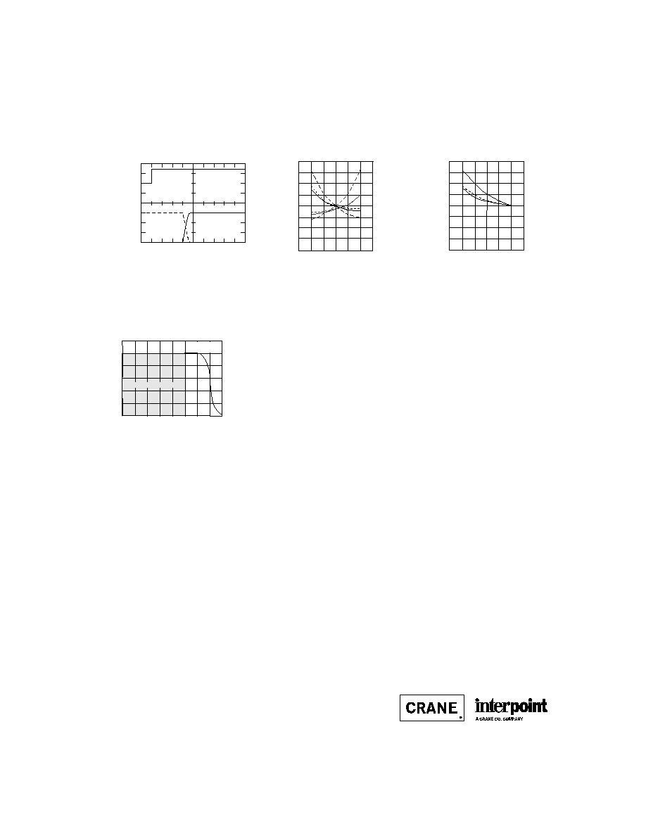
Typical Performance Curves: 25∞C Tc , 28 VDC Vin, 100% load, unless otherwise specified.
EFFICIENCY
30
80
40
50
60
70
0
0.25
0.5 0.75
1
1.25 1.5
OUTPUT POWER
ALL 5 VOLT MODELS
12 VOLT
28 VOLT
EFFICIENCY vs LINE & LOAD
50 VOLT
1.75
90
F
IGURE
3
1.75
EFFICIENCY
30
80
40
50
60
70
0
0.25
0.5 0.75
1
1.25 1.5
OUTPUT POWER
12 & 15 V SINGLES
12 VOLT
28 VOLT
50 VOLT
90
EFFICIENCY vs LINE & LOAD
F
IGURE
4
1.75
EFFICIENCY
30
80
40
50
60
70
0
0.25
0.5 0.75
1
1.25 1.5
OUTPUT POWER
12 & 15 V DUAL MODELS
12 VOLT
28 VOLT
50 VOLT
90
EFFICIENCY vs LINE & LOAD
F
IGURE
5
F
IGURE
9
F
IGURE
11
2V/div.
V
in
20V/div.
V
out
TURN-ON INTO FULL LOAD
0
2
4
6
8
10
12
14
16 18
TIME (ms)
MGH2805S
Representative of all 5 volt models
LOAD TRANSIENT RESPONSE
200 mV / div.
500
s / div.
MGH2815D
+V
OUT
FULL LOAD TO HALF LOAD
+V
OUT
HALF LOAD TO FULL LOAD
≠V
OUT
FULL LOAD TO HALF LOAD
≠V
OUT
HALF LOAD TO FULL LOAD
1
0
20
40
60
80
100
ATTENUATION (dB)
AUDIO REJECTION
10
60
FREQUENCY (kHz)
MGH2815S - Representative of all models
F
IGURE
6
V
in
LINE TRANSIENT RESPONSE
100 mV / div.
200 s / div.
20 V / div.
V
out
MGH2805S
12 VDC
50 VDC
F
IGURE
7
V
in
LINE TRANSIENT RESPONSE
200 mV / div.
200 s / div.
20 V / div.
+V
out
MGH2815D
≠V
out
12 VDC
50 VDC
F
IGURE
10
F
IGURE
8
LOAD TRANSIENT RESPONSE
100 mV / div.
500 s / div.
MGH2805S
HALF LOAD TO FULL LOAD
FULL LOAD TO HALF LOAD
B2-98
MGH SERIES
1.5 WATT
DC/DC C
ONVERTERS
Typical Performance Curves: 25∞C Tc , 28 VDC Vin, 100% load, unless otherwise specified.
5V/div.
V
in
20V/div.
≠V
out
TURN-ON INTO FULL LOAD
0
5
10
15
20
25
30
35
40 45
TIME (ms)
MGH2815D
Also representative of MGH2812S & D and MGH2815S
+V
out
0 V for ≠V
out
0 V for +V
out
F
IGURE
12
≠5
≠12
≠15
±
Vout VOLTAGE CHANGE (%)
4
-4
-2
0
2
90/10 70/30 50/50 30/70 10/90
OUTPUT LOAD (%)
DUAL
CROSS REGULATION
90% TO 10% LOAD ON +V
10% TO 90% LOAD ON ≠V
+5
+12
+15
F
IGURE
13
F
IGURE
14
20
±
V
out
VOLTAGE CHANGE (%)
4
-4
-2
0
2
10
30
40
50
OUTPUT LOAD (%)
DUAL
±
5
±
12
±
15
CROSS REGULATION
50% LOAD +V; 50% TO 10% LOAD ≠V
AND
50% LOAD ≠V; 50% TO 10% LOAD +V
SAFE OPERATING AREA
120
100
80
60
40
20
0
V
out
NOMINAL %
% OF FULL LOAD
OUTPUT VOLTAGE vs. OUTPUT LOAD
0
20
40
60
80
100 120 140
160
TRIP POINT
125%
F
IGURE
15
22622-001-DTS Rev A
DQ# 1033
All technical information is believed to be accurate, but no responsibility is
assumed for errors or omissions. Interpoint reserves the right to make changes in
products or specifications without notice. MGH Series is a trademark of Interpoint.
Copyright © 1998 - 1999 Interpoint. All rights reserved.

1.000
(25.40)
0.870 (22.10)
0.060 (1.52)
0.075 (1.91)
0.030 (0.76)
0.100 (2.54) 4X
0.100 (2.54) 16X
B8-7
CASE B
C
ASES
CASE B
TOP VIEW
See Figure 6
for pin
configurations.
0.880 max
(22.35)
Materials
Header
Kovar/Nickel/Gold
Cover Kovar/Nickel
Pins Kovar/Nickel/Gold,
matched glass seal
Case dimensions in inches (mm)
Tolerance
±
0.005 (0.13) for three decimal places
±
0.01 (0.3) for two decimal places
unless otherwise specified
Cover marking is oriented with pin one
at the upper right corner.
1.010 max
(25.65)
CAUTION
Maximum reflow temperature is 220
∞
C for a
maximum of 30 seconds. SN60, SN62, or SN63
are the recommended types of solder. See below
for Solder Mask instructions.
Hand soldering should not exceed 300
∞
C for 10
seconds per pin.
Differently colored glass bead around pin one or dimple
in header (bottom or side of case) indicates pin one.
(This view shows
straight leads.)
Gull Wing Leads
Option
0.135 ref. (3.43)
Gull wing leads are solder dipped.
Lead dimensions are prior to solder dip.
0.08
(2.0)
0.010 (0.25)
Bottom of case to
bottom of lead
0.055
(1.40)
0.070
(1.78)
0.08 (2.0)
1.140 ref. (28.96)
1
1
FMGA EMI Filter: Screening ≠ Standard, ES, or 883
MGH Series: Screening ≠ Standard, ES, or 883
TOP VIEW CASE B
0.010
(0.25)
1.870 ref. (47.50)
0.015
(0.38)
0.010
(0.25)
0.900 (22.86)
0.800 (20.32)
0.700 (17.78)
0.600 (15.24)
0.500 (12.70)
0.400 (10.16)
0.300 ( 7.62)
Differently colored glass bead around pin one or dimple in
header (bottom or side of case) indicates pin one.
Cover marking is oriented with pin one at the upper right corn
1
2
3
4
5
6
8
9
7
18
17
16
15
14
13
12
11
10
0.000
0.000
Straight Leads
0.50
(12.7)
0.250 max.
(6.35)
0.200 ( 5.08)
0.100 ( 2.54)
Seam seal
Solder Mask Notes
1. Pad dimensions are for the solder mask opening. Lead common to
each other can be connected underneath as desired.
2. Ground pins should be connected to the center pad for improved
grounding.
3. Center pad should not have a solder mask. Solder, copper, or Au/Ni
plate are preferred over solder for adhesive attach.
4. Solder coat to solder down converter.
5. If less rotation of case is desired, make the pad width 0.020inches
(0.51 mm). Pad length can be extended 0.010 inches (0.25 mm)
towards the case body and as-desired dimension away from the case
body.
6. Do not exceed 220∞C as measured on the body of the converter (top
or bottom).
7. Attach the body of the case to the board with a thermally conductive
adhesive or SN60, 62, or 63 solder. The adhesive can be electrically
conductive as well. It can be applied as an underfill post solder or
dispensed and cured prior or during solder.
Note: Although every effort has been made to render the case drawings at actual size, variations in the printing process may cause some distortion. Please refer
to the numerical dimensions for accuracy.
F
IGURE
6: C
ASE
B
F
IGURE
7: C
ASE
B S
OLDER
M
ASK
F
IGURE
5: C
ASE
B M
AXIMUM
D
IMENSIONS

C2-10
TEST (125∞C Products)
STANDARD
/ES
/883 (Class H)*
PRE-CAP INSPECTION
Method 2017, 2032
yes
yes
yes
TEMPERATURE CYCLE (10 times)
Method 1010, Cond. C, -65∞C to 150∞C
no
no
yes
Method 1010, Cond. B, -55∞C to 125∞C
no
yes
no
CONSTANT ACCELERATION
Method 2001, 3000 g
no
no
yes
Method 2001, 500 g
no
yes
no
BURN-IN
Method 1015, 160 hours at 125∞C
no
no
yes
96 hours at 125∞C case (typical)
no
yes
no
FINAL ELECTRICAL TEST MIL-PRF-38534, Group A
Subgroups 1 through 6: -55∞C, +25∞C, +125∞C
no
no
yes
Subgroups 1 and 4: +25∞C case
yes
yes
no
HERMETICITY TESTING
Fine Leak, Method 1014, Cond. A
no
yes
yes
Gross Leak, Method 1014, Cond. C
no
yes
yes
Gross Leak, Dip (1 x 10
-3
)
yes
no
no
FINAL VISUAL INSPECTION
Method 2009
yes
yes
yes
Test methods are referenced to MIL-STD-883 as determined by MIL-PRF-38534.
*883 products are built with element evaluated components and are 100% tested and guaranteed over
the full military temperature range of ≠55∞C to +125∞C.
MOR Series
MFLHP Series
MFL Series
MHP Series
MTR Series
MQO Series**
MHD Series
MHV Series
MHF+ Series
MHF Series**
MGA Series
MSA Series
MGH Series
MCH Series
FM-704A EMI Filter
FMD**/FME EMI Filter
FMC EMI Filter
FMH EMI Filter
FMGA EMI Filter
FMSA EMI Filter
HUM Modules**
LCM Modules**
LIM Modules
QA SCREENING
125∞C PRODUCTS
125∞C P
RODUCTS
Applies to the following products
**MFLHP Series, MQO Series, MHF Series, FMD EMI Filters, Hum Modules, and LCM Modules do not offer
`883" screening.