1
File Number
4014.1
CAUTION: These devices are sensitive to electrostatic discharge; follow proper IC Handling Procedures.
1-888-INTERSIL or 321-724-7143 | Copyright © Intersil Corporation 1999
HS-2620RH, HS-2622RH
Radiation Hardened, Very Wideband, High
Input Impedance Uncompensated
Operational Amplifiers
HS-2620RH and HS-2622RH are radiation hardened bipolar
operational amplifiers that feature very high input impedance
coupled with wideband AC performance. The high resistance
of the input stage is complemented by low offset voltage (4mV
Max at 25
o
C for HS-2620RH) and low bias and offset current
(15nA Max at 25
o
C for HS-2620RH) to facilitate accurate
signal processing. Offset voltage can be reduced further by
means of an external nulling potentiometer. Closed loop gains
greater than 5, the 25V/
µ
s minimum slew rate at 25
o
C and the
100kV/V minimum open loop gain at 25
o
C, enables the
HS-2620RH to perform high gain amplification of very fast,
wideband signals. These dynamic characteristics, coupled
with fast settling times, make these amplifiers ideally suited to
pulse amplification designs as well as high frequency or video
applications. The frequency response of the amplifier can be
tailored to exact design requirements by means of an external
bandwidth control capacitor. Other high performance designs
such as high gain, low distortion audio amplifiers, high-Q and
wideband active filters and high speed comparators are
excellent uses of this part.
Specifications for Rad Hard QML devices are controlled
by the Defense Supply Center in Columbus (DSCC). The
SMD numbers listed here must be used when ordering.
Detailed Electrical Specifications for these devices are
contained in SMD 5962-95688. A "hot-link" is provided
on our homepage for downloading.
www.intersil.com/spacedefense/space.asp
Features
∑ Electrically Screened to SMD # 5962-95688
∑ QML Qualified per MIL-PRF-38535 Requirements
∑ High Input Impedance (HS-2620RH) . . . . . . . 65M
(Min)
∑ High Gain (HS-2620RH) . . . . . . . . . . . . . . . . 100kV/V (Min)
150kV/V (Typ)
∑ High Slew Rate (HS-2620RH) . . . . . . . . . . . . . . 25V/
µ
s (Min)
35V/
µ
s (Typ)
∑ Low Input Bias Current (HS-2620RH) . . . . . . . 15nA (Max)
5nA (Typ)
∑ Low Input Offset Voltage (HS-2620RH) . . . . . . 4mV (Max)
∑ Wide Gain Bandwidth Product (AV
5) . . . . . .100MHz (Typ)
∑ Output Short Circuit Protection
∑ Total Dose . . . . . . . . . . . . . . . . . . . . . . . . . . . 1 x 10
4
RAD(Si)
Applications
∑ Video and RF Amplifiers
∑ Pulse Amplifiers
∑ Audio Amplifiers and Filters
∑ High-Q Active Filters
∑ High Speed Comparators
Ordering Information
ORDERING NUMBER
INTERNAL
MKT. NUMBER
TEMP. RANGE
(
o
C)
5962D9568801VGA
HS2-2620RH-Q
-55 to 125
5962D9568801VPA
HS7-2620RH-Q
-55 to 125
5962D9568801VPC
HS7B-2620RH-Q
-55 to 125
5962D9568802VGA
HS2-2622RH-Q
-55 to 125
5962D9568802VPA
HS7-2622RH-Q
-55 to 125
5962D9568802VPC
HS7B-2622RH-Q
-55 to 125
Pinouts
HS7-2620RH, HS7-2622RH (CERDIP) GDIP1-T8
OR
HS7B-2620RH, HS7B-2622RH (SBDIP) CDIP2-T8
TOP VIEW
HS2-2620RH, HS2-2622RH (CAN) MACY1-X8
TOP VIEW
BAL
-IN
+IN
V-
1
2
3
4
8
7
6
5
COMP
V+
OUT
BAL
-
+
COMP
OUT
IN-
V-
BAL
IN+
V+
BAL
2
4
6
1
3
7
5
8
-
+
Data Sheet
August 1999

2
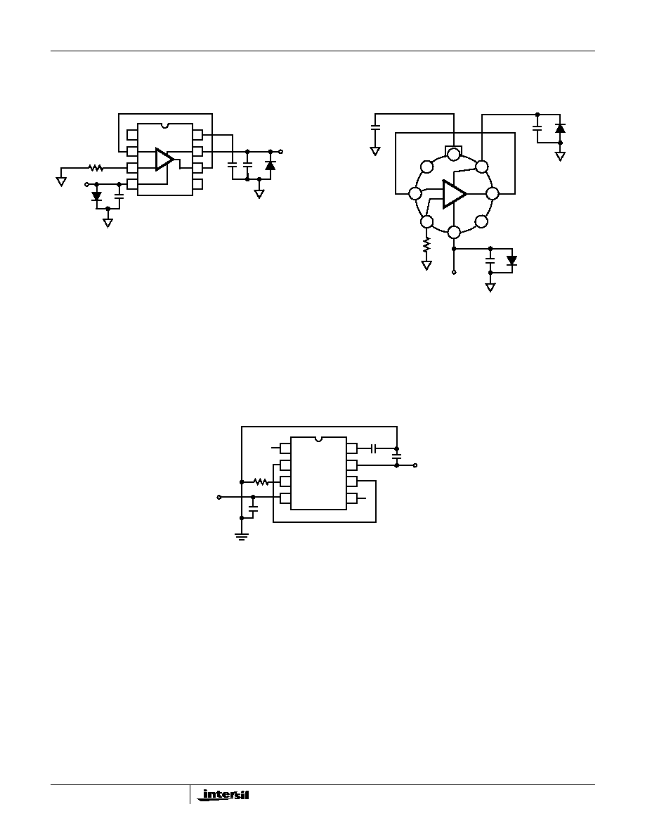
Test Circuit
NOTE: Includes stray capacitances.
FIGURE 1. TEST LOOP FOR THE HS-2620RH AND THE HS-2622RH
S5A
2
1
VAC
100
100
+VCC
S5B
2
1
+
OPEN 1
2
3
S8
2K
10K
-VEE
OPEN
S9
1
2
50
50pF (NOTE)
1
+
V2
EOUT
S4
2
1
5K
50K
1
100K
S1
+
50K
V1
S2
S6
1
2
DUT
S3B
2
OPEN
1
1
0.1
2
3
OPEN
1
S7
RAL
ADJ
500K
BUFFER
FOR LOOP STABILITY,
USE MIN VALUE CAPACITOR
TO PREVENT OSCILLATION
OPEN 2
OPEN 2
100K
S3A
1
0.1
x 2
400
1.6K
1 OPEN
2
ALL RESISTORS =
±
1% (
)
ALL CAPACITORS =
±
10% (
µ
F)
-1/10
-
-
ACOUT
-
1
Test Circuits and Waveforms
FIGURE 2. SIMPLIFIED TEST CIRCUIT
FIGURE 3. SLEW RATE WAVEFORM
NOTE: Measured on both positive and negative transitions. Capacitance at Compensation pin should be minimized.
FIGURE 4. OVERSHOOT, RISE AND FALL TIME WAVEFORMS
50pF
+
1.6K
400
VAC IN
VAC OUT
50
-
+5.0V
-5.0V
T
+5.0V
-5.0V
T
T
V
SR =
V
OUTPUT
V
+1.0V
-1.0V
+1.0V
-1.0V
INPUT
+SL
-SL
+40mV
0V
0V
-40mV
INPUT
t
r
, +OS
t
f
, -OS
OUTPUT
90%
t
r
t
f
VPEAK
VFINAL = +200mV
-200mV
10%
0V
10%
0V
90%
VPEAK
HS-2620RH, HS-2622RH

5
All Intersil semiconductor products are manufactured, assembled and tested under ISO9000 quality systems certification.
Intersil semiconductor products are sold by description only. Intersil Corporation reserves the right to make changes in circuit design and/or specifications at any time with-
out notice. Accordingly, the reader is cautioned to verify that data sheets are current before placing orders. Information furnished by Intersil is believed to be accurate and
reliable. However, no responsibility is assumed by Intersil or its subsidiaries for its use; nor for any infringements of patents or other rights of third parties which may result
from its use. No license is granted by implication or otherwise under any patent or patent rights of Intersil or its subsidiaries.
For information regarding Intersil Corporation and its products, see web site http://www.intersil.com
Die Characteristics
DIE DIMENSIONS:
69 mils x 66 mils x 19 mils
±
1 mil
1750
µ
m x 1420
µ
m x 483
µ
m
±
25.4
µ
m
INTERFACE MATERIALS:
Glassivation:
Type: Nitride (S13N4) over Silox (SiO2, 5% Phos.)
Silox Thickness: 12k
≈
±
2k
≈
Nitride Thickness: 3.5k
≈
±
1.5k
≈
Top Metallization:
Type: Al, 1% Cu
Thickness: 18k
≈
±
2k
≈
Substrate:
Linear Bipolar, DI
Backside Finish:
Silicon
ASSEMBLY RELATED INFORMATION:
Substrate Potential (Powered Up):
Unbiased
ADDITIONAL INFORMATION:
Worst Case Current Density:
<2 x 10
5
A/cm
2
Transistor Count:
HS-2620RH: 140
HS-2622RH: 140
Metallization Mask Layout
HS-2620RH, HS-2622RH
BAL
-IN
+IN
V-
BAL
OUT
V+
COMP
HS-2620RH, HS-2622RH