
1
Æ
FN9001.3
CAUTION: These devices are sensitive to electrostatic discharge; follow proper IC Handling Procedures.
1-888-INTERSIL or 321-724-7143
|
Intersil (and design) is a registered trademark of Intersil Americas Inc.
Copyright © Intersil Americas Inc. 2003. All Rights Reserved.
All other trademarks mentioned are the property of their respective owners.
IS-1845ASRH
Single Event Radiation Hardened
High Speed, Current Mode PWM
The IS-1845ASRH is designed to be
used in switching power supplies
operating in current-mode. The
rising edge of the on-chip oscillator
turns on the output. Turn-off is controlled by the current
sense comparator and occurs when the sensed current
reaches a peak controlled by the error amplifier.
Constructed with Intersil's Rad Hard Silicon Gate (RSG)
dielectrically isolated BiCMOS process, these devices are
immune to single event latch-up and have been specifically
designed to provide a high level of immunity to single event
transients. All specified parameters are guaranteed and
tested for 300krad(Si) total dose performance.
Detailed Electrical Specifications for these devices are
contained in SMD 5962-01509. A "hot-link" is provided on
our website for downloading the SMD.
Pinouts
IS7-1845ASRH (CDIP2-T8 SBDIP)
TOP VIEW
IS9-1845ASRH (FLATPACK)
TOP VIEW
NOTES:
1. Grounding the Comp pin does not inhibit the output. The output
may be inhibited by applying >1.2V to the ISENSE pin.
2. This part should be operated with CT=3.3nF and RT=10k timing
components only.
Features
∑ Electrically Screened to DSCC SMD # 5962-01509
∑ QML Qualified per MIL-PRF-38535 Requirements
∑ Radiation Environment
- Total Dose . . . . . . . . . . . . . . . . . . . . 300 krad(SI) (Max)
- SEL Immune. . . . . . . . . . . . . . . . . Dielectrically Isolated
- SEU Immune . . . . . . . . . . . . . . . . . . . . 35MeV/mg/cm
2
- SEU Cross-Section at 89MeV/mg/cm
2
. . . . 5 x 10
-6
cm
2
∑ Low Start-up Current . . . . . . . . . . . . . . . . . . . 100
µ
A (Typ)
∑ Fast Propagation Delay . . . . . . . . . . . . . . . . . . 80ns (Typ)
∑ Supply Voltage Range . . . . . . . . . . . . . . . . . . . 12V to 20V
∑ High Output Drive. . . . . . . . . . . . . . . . . . . . 1A (Peak, Typ)
∑ Under Voltage Lockout. .8.8V Start (Typ), 8.2V Stop (Typ)
Applications
∑ Current-Mode Switching Power Supplies
∑ Control of High Current FET Drivers
∑ Motor Speed and Direction Control
TM
COMP
VFB
ISENSE
RTCT
1
2
3
4
8
7
6
5
VREF
VCC
OUT
GND
COMP
VFB
NC
NC
NC
ISENSE
RTCT
NC
3
4
5
6
7
8
9
2
17
16
15
14
13
12
11
10
VREF
VCC
VC
OUT
NC
GND
OSCGND
NC
NC
1
18
NC
Ordering Information
ORDERING NUMBER
INTERNAL
MKT. NUMBER
TEMP. RANGE
(
o
C)
5962F0150901VPC
IS7-1845ASRH-Q
-50 to 125
5962F0150901QPC
IS7-1845ASRH-8
-50 to 125
5962F0150901VXC
IS9-1845ASRH-Q
-50 to 125
5962F0150901QXC
IS9-1845ASRH-8
-50 to 125
IS7-1845ASRH/Proto
IS1-1845ASRH/Proto
-50 to 125
IS9-1845ASRH/Proto
IS9-1845ASRH/Proto
-50 to 125
Data Sheet
October 2003
2
All Intersil U.S. products are manufactured, assembled and tested utilizing ISO9000 quality systems.
Intersil Corporation's quality certifications can be viewed at www.intersil.com/design/quality
Intersil products are sold by description only. Intersil Corporation reserves the right to make changes in circuit design, software and/or specifications at any time without
notice. Accordingly, the reader is cautioned to verify that data sheets are current before placing orders. Information furnished by Intersil is believed to be accurate and
reliable. However, no responsibility is assumed by Intersil or its subsidiaries for its use; nor for any infringements of patents or other rights of third parties which may result
from its use. No license is granted by implication or otherwise under any patent or patent rights of Intersil or its subsidiaries.
For information regarding Intersil Corporation and its products, see www.intersil.com
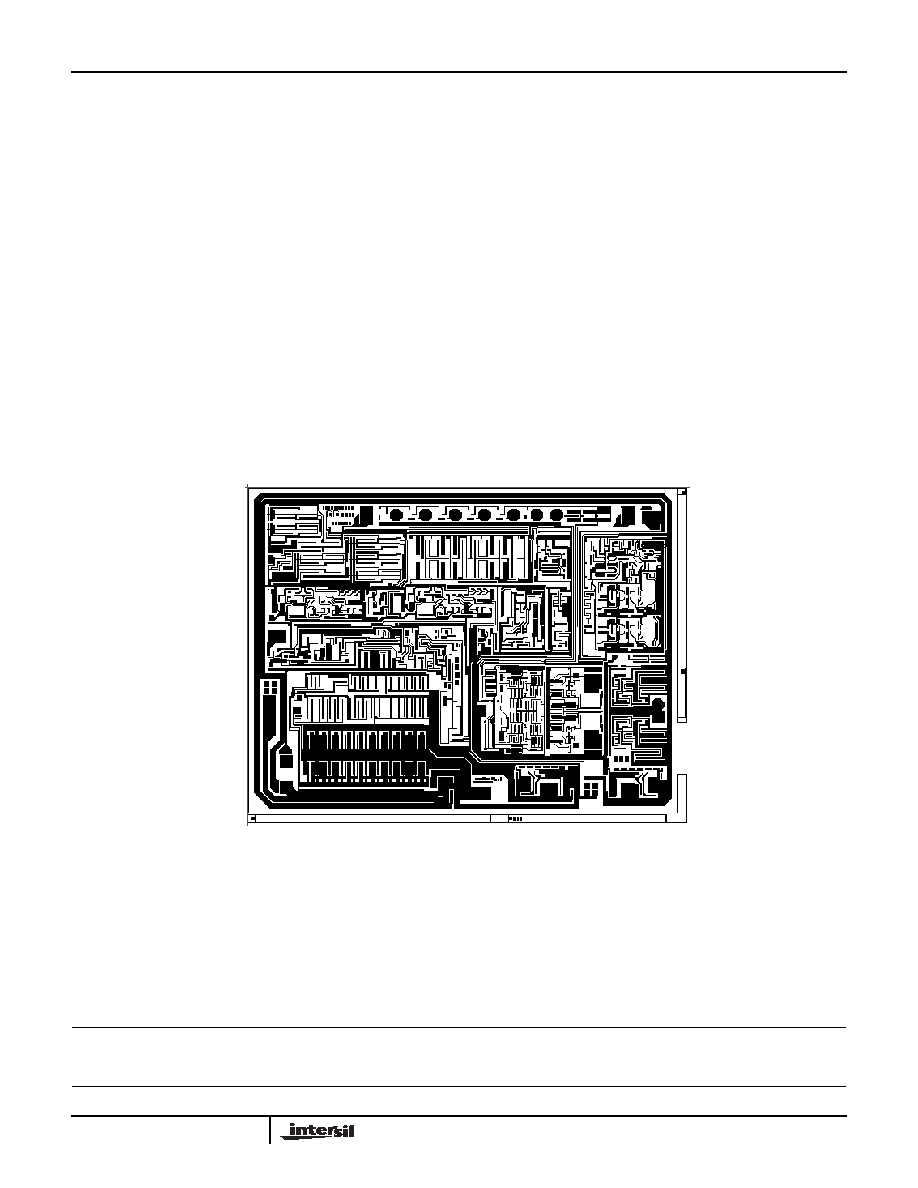
Die Characteristics
DIE DIMENSIONS
3090
µ
m x 4080
µ
m (121.6 mils x 159.0 mils)
Thickness: 483
µ
m
±
25.4
µ
m (19 mils
±
1 mil)
INTERFACE MATERIALS
Glassivation
Type: Phosphorus Silicon Glass (PSG)
Thickness: 8.0kA
±
1.0kA
Top Metallization
Type: AlSiCu
Thickness: 16.0kA
±
2kA
Substrate
Radiation Hardened Silicon Gate,
Dielectric Isolation
Backside Finish
Silicon
ASSEMBLY RELATED INFORMATION
Substrate Potential
Unbiased (DI)
ADDITIONAL INFORMATION
Worst Case Current Density
<2.0 x 10
5
A/cm
2
Transistor Count
582
Metallization Mask Layout
IS-1845ASRH
NOTES:
3. Both the GND pads must be bonded to ground.
4. The OUT double-sized bond pad must be double bonded for
current sharing purposes.
5. The OSCGND double-sized bond pad must be double bonded to
ground for current sharing purposes.
VFB
COMP
VREF
VC
VCC
OUT
GND
GND
OSCGND
RTCT
ISENSE
IS-1845ASRH