1
File Number
4228.1
CAUTION: These devices are sensitive to electrostatic discharge; follow proper IC Handling Procedures.
1-888-INTERSIL or 321-724-7143 | Copyright © Intersil Corporation 1999
HS-1212RH
Radiation Hardened, Dual, High Speed
Low Power, Video Closed Loop Buffer
The HS-1212RH is a dual closed loop buffer featuring user
programmable gain and high speed performance.
Manufactured on Intersil's proprietary complementary
bipolar UHF-1 (DI bonded wafer) process, this device offers
wide -3dB bandwidth of 340MHz, very fast slew rate,
excellent gain flatness and high output current. These
devices are QML approved and are processed and screened
in full compliance with MIL-PRF-38535.
A unique feature of the pinout allows the user to select a
voltage gain of +1, -1, or +2, without the use of any external
components. Gain selection is accomplished via
connections to the inputs, as described in the "Application
Information" section. The result is a more flexible product,
fewer part types in inventory, and more efficient use of board
space.
Compatibility with existing op amp pinouts provides flexibility
to upgrade low gain amplifiers, while decreasing component
count. Unlike most buffers, the standard pinout provides an
upgrade path should a higher closed loop gain be needed at
a future date.
Specifications for Rad Hard QML devices are controlled
by the Defense Supply Center in Columbus (DSCC). The
SMD numbers listed here must be used when ordering.
Detailed Electrical Specifications for these devices are
contained in SMD 5962-96831. A "hot-link" is provided
on our homepage for downloading.
www.intersil.com/spacedefense/space.asp
Features
∑ Electrically Screened to SMD # 5962-96831
∑ QML Qualified per MIL-PRF-38535 Requirements
∑ MIL-PRF-38535 Class V Compliant
∑ User Programmable For Closed-Loop Gains of +1, -1 or
+2 Without Use of External Resistors
∑ Standard Operational Amplifier Pinout
∑ Low Supply Current . . . . . . . . . . . . 5.9mA/Op Amp (Typ)
∑ Excellent Gain Accuracy . . . . . . . . . . . . . . . 0.99V/V (Typ)
∑ Wide -3dB Bandwidth. . . . . . . . . . . . . . . . . .340MHz (Typ)
∑ Fast Slew Rate . . . . . . . . . . . . . . . . . . . . . .1155V/
µ
s (Typ)
∑ High Input Impedance . . . . . . . . . . . . . . . . . . . 1M
(Typ)
∑ Excellent Gain Flatness (to 50MHz) . . . . . .
±
0.02dB (Typ)
∑ Fast Overdrive Recovery . . . . . . . . . . . . . . . . <10ns (Typ)
∑ Total Gamma Dose. . . . . . . . . . . . . . . . . . . . 300kRAD(Si)
∑ Latch Up . . . . . . . . . . . . . . . . . . . . . None (DI Technology)
Applications
∑ Flash A/D Driver
∑ Video Switching and Routing
∑ Pulse and Video Amplifiers
∑ Wideband Amplifiers
∑ RF/IF Signal Processing
∑ Imaging Systems
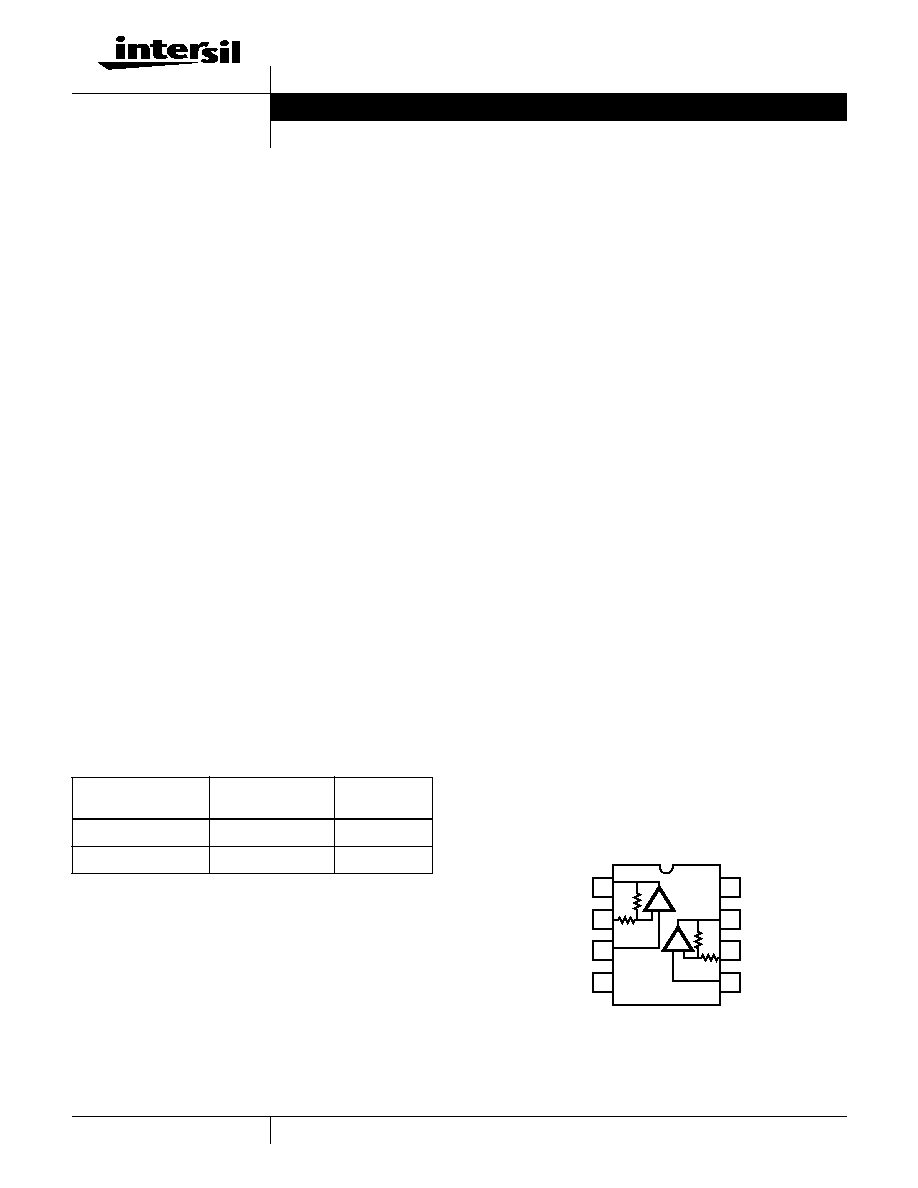
Pinout
HS-1212RH (CERDIP) GDIP1-T8
OR
HS-1212RH (SBDIP) CDIP2-T8
TOP VIEW
Ordering Information
ORDERING NUMBER
INTERNAL
MKT. NUMBER
TEMP. RANGE
(
o
C)
5962F9683101VPA
HS7-1212RH-Q
-55 to 125
5962F9683101VPC
HS7B-1212RH-Q
-55 to 125
OUT1
-IN1
+IN1
V-
1
2
3
4
8
7
6
5
V+
OUT2
-IN2
+IN2
+
-
+ -
Data Sheet
August 1999
2
Application Information
HS-1212RH Advantages
The HS-1212RH features a novel design which allows the
user to select from three closed loop gains, without any
external components. The result is a more flexible product,
fewer part types in inventory, and more efficient use of board
space. Implementing a dual, gain of 2, cable driver with this
IC eliminates the four gain setting resistors, which frees up
board space for termination resistors.
Like most newer high performance amplifiers, the
HS-1212RH is a current feedback amplifier (CFA). CFAs
offer high bandwidth and slew rate at low supply currents,
but can be difficult to use because of their sensitivity to
feedback capacitance and parasitics on the inverting input
(summing node). The HS-1212RH eliminates these
concerns by bringing the gain setting resistors on-chip. This
yields the optimum placement and value of the feedback
resistor, while minimizing feedback and summing node
parasitics. Because there is no access to the summing node,
the PCB parasitics do not impact performance at gains of +2
or -1 (see "Unity Gain Considerations" for discussion of
parasitic impact on unity gain performance).
The HS-1212RH's closed loop gain implementation provides
better gain accuracy, lower offset and output impedance,
and better distortion compared with open loop buffers.
Closed Loop Gain Selection
This "buffer" operates in closed loop gains of -1, +1, or +2, with
gain selection accomplished via connections to the inputs.
Applying the input signal to +IN and floating -IN selects a gain
of +1 (see next section for layout caveats), while grounding -IN
selects a gain of +2. A gain of -1 is obtained by applying the
input signal to -IN with +IN grounded through a 50
resistor.
The table below summarizes these connections:
Unity Gain Considerations
Unity gain selection is accomplished by floating the -Input of
the HS-1212RH. Anything that tends to short the -Input to
GND, such as stray capacitance at high frequencies, will
cause the amplifier gain to increase toward a gain of +2. The
result is excessive high frequency peaking, and possible
instability. Even the minimal amount of capacitance
associated with attaching the -Input lead to the PCB results
in approximately 6dB of gain peaking. At a minimum this
requires due care to ensure the minimum capacitance at the
-Input connection.
Table 1 lists five alternate methods for configuring the
HS-1212RH as a unity gain buffer, and the corresponding
performance. The implementations vary in complexity and
involve performance trade-offs. The easiest approach to
implement is simply shorting the two input pins together,
and applying the input signal to this common node. The
amplifier bandwidth decreases from 430MHz to 280MHz,
but excellent gain flatness is the benefit. A drawback to this
approach is that the amplifier input noise voltage and input
offset voltage terms see a gain of +2, resulting in higher
noise and output offset voltages. Alternately, a 100pF
capacitor between the inputs shorts them only at high
frequencies, which prevents the increased output offset
voltage but delivers less gain flatness.
Another straightforward approach is to add a 620
resistor
in series with the amplifier's positive input. This resistor and
the HS-1212RH input capacitance form a low pass filter
which rolls off the signal bandwidth before gain peaking
occurs. This configuration was employed to obtain the data
sheet AC and transient parameters for a gain of +1.
Pulse Overshoot
The HS-1212RH utilizes a quasi-complementary output stage
to achieve high output current while minimizing quiescent
supply current. In this approach, a composite device replaces
the traditional PNP pulldown transistor. The composite device
switches modes after crossing 0V, resulting in added distortion
for signals swinging below ground, and an increased overshoot
on the negative portion of the output waveform (see Figure 6,
Figure 9, and Figure 12). This overshoot isn't present for small
bipolar signals (see Figure 4, Figure 7, and Figure 10) or large
positive signals (see Figure 5, Figure 8 and Figure 11).
PC Board Layout
This amplifier's frequency response depends greatly on the
care taken in designing the PC board (PCB). The use of low
inductance components such as chip resistors and chip
capacitors is strongly recommended, while a solid
ground plane is a must!
Attention should be given to decoupling the power supplies.
A large value (10
µ
F) tantalum in parallel with a small value
(0.1
µ
F) chip capacitor works well in most cases.
GAIN
(A
CL
)
CONNECTIONS
+INPUT
-INPUT
-1
50
to GND
Input
+1
Input
NC (Floating)
+2
Input
GND
HS-1212RH
3
Terminated microstrip signal lines are recommended at the
input and output of the device. Capacitance directly on the
output must be minimized, or isolated as discussed in the
next section.
An example of a good high frequency layout is the
Evaluation Board shown in Figure 3.
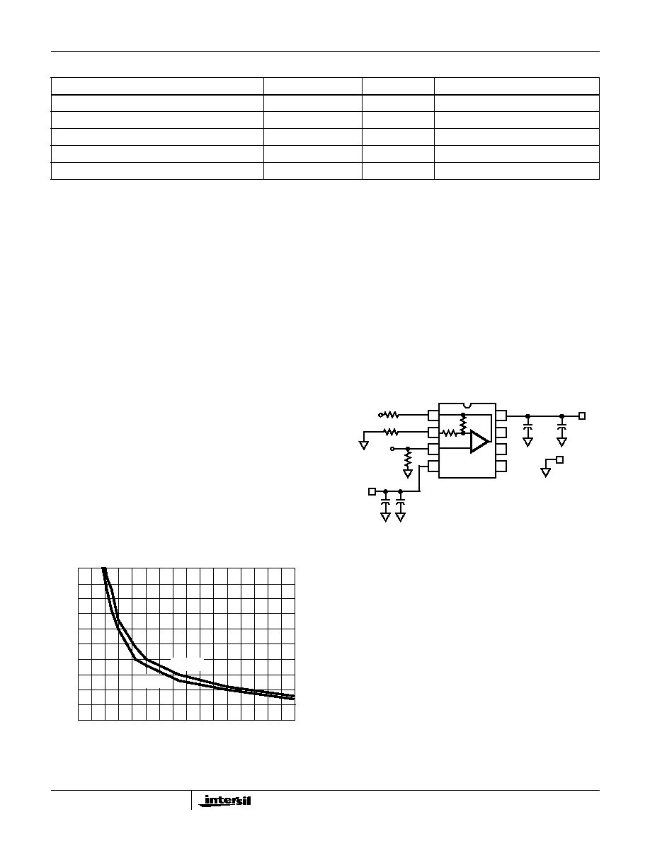
Driving Capacitive Loads
Capacitive loads, such as an A/D input, or an improperly
terminated transmission line will degrade the amplifier's
phase margin resulting in frequency response peaking and
possible oscillations. In most cases, the oscillation can be
avoided by placing a resistor (R
S
) in series with the output
prior to the capacitance.
Figure 1 details starting points for the selection of this
resistor. The points on the curve indicate the R
S
and C
L
combinations for the optimum bandwidth, stability, and
settling time, but experimental fine tuning is recommended.
Picking a point above or to the right of the curve yields an
overdamped response, while points below or left of the curve
indicate areas of underdamped performance.
R
S
and C
L
form a low pass network at the output, thus
limiting system bandwidth well below the amplifier bandwidth
of 350MHz. By decreasing R
S
as C
L
increases (as
illustrated in the curves), the maximum bandwidth is
obtained without sacrificing stability. In spite of this,
bandwidth decreases as the load capacitance increases.
Evaluation Board
The performance of the HS-1212RH may be evaluated using
the HA5023 Evaluation Board, slightly modified as follows:
1. Remove the two feedback resistors, and leave the
connections open.
2. a. For A
V
= +1 evaluation, remove the gain setting
resistors (R
1
), and leave pins 2 and 6 floating.
b. For A
V
= +2, replace the gain setting resistors (R
1
)
with 0
resistors to GND.
The modified schematic for amplifier 1, and the board layout
are shown in Figures 2 and 3.
To order evaluation boards (part number HA5023EVAL),
please contact your local sales office.
TABLE 1. UNITY GAIN PERFORMANCE FOR VARIOUS IMPLEMENTATIONS
APPROACH
PEAKING (dB)
BW (MHz)
±
0.1dB GAIN FLATNESS (MHz)
Remove -IN Pin
4.5
430
21
+R
S
= 620
0
220
27
+R
S
= 620
and Remove -IN Pin
0.5
215
15
Short +IN to -IN (e.g., Pins 2 and 3)
0.6
280
70
100pF Capacitor Between +IN and -IN
0.7
290
40
0
100
200
300
400
0
10
20
30
40
50
LOAD CAPACITANCE (pF)
SERIES OUTPUT RESIST
ANCE (
)
A
V
= +2
150
250
350
50
A
V
= +1
FIGURE 1. RECOMMENDED SERIES RESISTOR vs LOAD
CAPACITANCE
-
5V
10
µ
F
0.1
µ
F
50
GND
GND
R
1
+
5V
0.1
µ
F
10
µ
F
50
IN
OUT
(A
V
= +
1)
OR 0
(A
V
= +
2)
NOTE: R
1
=
FIGURE 2. MODIFIED EVALUATION BOARD SCHEMATIC
+
-
(NOTE)
1
2
3
4
8
7
6
5
HS-1212RH

4
FIGURE 3A. TOP LAYOUT
FIGURE 3B. BOTTOM LAYOUT
FIGURE 3. EVALUATION BOARD LAYOUT
Typical Performance Curves
V
SUPPLY
=
±
5V, T
A
= 25
o
C, R
L
= 100
, Unless Otherwise Specified
FIGURE 4. SMALL SIGNAL PULSE RESPONSE
FIGURE 5. LARGE SIGNAL POSITIVE PULSE RESPONSE
FIGURE 6. LARGE SIGNAL BIPOLAR PULSE RESPONSE
FIGURE 7. SMALL SIGNAL PULSE RESPONSE
TIME (5ns/DIV.)
OUTPUT V
O
L
T
A
GE (mV)
200
150
100
50
0
-50
-100
-150
-200
A
V
= +2
TIME (5ns/DIV.)
OUTPUT V
O
L
T
A
GE (V)
2.0
1.5
1.0
0.5
0
-0.5
-1.0
-1.5
-2.0
A
V
= +2
TIME (5ns/DIV.)
OUTPUT V
O
L
T
A
GE (V)
2.0
1.5
1.0
0.5
0
-0.5
-1.0
-1.5
-2.0
A
V
= +2
TIME (5ns/DIV.)
OUTPUT V
O
L
T
A
GE (mV)
200
150
100
50
0
-50
-100
-150
-200
A
V
= +1
HS-1212RH

5
FIGURE 8.
LARGE SIGNAL POSITIVE PULSE RESPONSE
FIGURE 9. LARGE SIGNAL BIPOLAR PULSE RESPONSE
FIGURE 10. SMALL SIGNAL PULSE RESPONSE
FIGURE 11.
LARGE SIGNAL POSITIVE PULSE RESPONSE
FIGURE 12. LARGE SIGNAL BIPOLAR PULSE RESPONSE
FIGURE 13. FREQUENCY RESPONSE
Typical Performance Curves
V
SUPPLY
=
±
5V, T
A
= 25
o
C, R
L
= 100
, Unless Otherwise Specified (Continued)
TIME (5ns/DIV.)
OUTPUT V
O
L
T
A
GE (V)
2.0
1.5
1.0
0.5
0
-0.5
-1.0
-1.5
-2.0
A
V
= +1
TIME (5ns/DIV.)
OUTPUT V
O
L
T
A
GE (V)
2.0
1.5
1.0
0.5
0
-0.5
-1.0
-1.5
-2.0
A
V
= +1
TIME (5ns/DIV.)
OUTPUT V
O
L
T
A
GE (mV)
200
150
100
50
0
-50
-100
-150
-200
A
V
= -1
TIME (5ns/DIV.)
OUTPUT V
O
L
T
A
GE (V)
2.0
1.5
1.0
0.5
0
-0.5
-1.0
-1.5
-2.0
A
V
= -1
TIME (5ns/DIV.)
OUTPUT V
O
L
T
A
GE (V)
2.0
1.5
1.0
0.5
0
-0.5
-1.0
-1.5
-2.0
A
V
= -1
PHASE
GAIN
1
10
100
600
FREQUENCY (MHz)
6
3
0
-3
-6
-9
NORMALIZED GAIN (dB)
A
V
= -1
A
V
= +1
A
V
= +2
A
V
= +1
A
V
= +2
-90
-180
-270
-360
0
NORMALIZED PHASE (DEGREES)
V
OUT
= 200mV
P-P
+R
S
= 620
(+1)
+R
S
= 0
(-1, +2)
HS-1212RH