1
ACS32MS
Radiation Hardened Quad 2-Input OR Gate
The Radiation Hardened ACS32MS is a Quad 2-Input OR
Gate. For each gate, a HIGH level on either A or B input
results in a HIGH level on the Y output. A LOW level on both
the A and B inputs results in a LOW level on the Y output. All
inputs are buffered and the outputs are designed for
balanced propagation delay and transition times.
The ACS32MS is fabricated on a CMOS Silicon on Sapphire
(SOS) process, which provides an immunity to Single Event
Latch-up and the capability of highly reliable performance in
any radiation environment. These devices offer significant
power reduction and faster performance when compared to
ALSTTL types.
Specifications for Rad Hard QML devices are controlled
by the Defense Supply Center in Columbus (DSCC). The
SMD numbers listed below must be used when ordering.
Detailed Electrical Specifications for the ACS32MS are
contained in SMD 5962-98624. A "hot-link" is provided
on our homepage with instructions for downloading.
www.intersil.com/data/sm/index.asp
Features
∑ QML Qualified Per MIL-PRF-38535 Requirements
∑ 1.25 Micron Radiation Hardened SOS CMOS
∑ Radiation Environment
- Latch-Up Free Under any Conditions
- Total Dose . . . . . . . . . . . . . . . . . . . . . . 3 x 10
5
RAD (Si)
- SEU Immunity . . . . . . . . . . . . . <1 x 10
-10
Errors/Bit/Day
- SEU LET Threshold . . . . . . . . . . . . >100MeV/(mg/cm
2
)
∑ Input Logic Levels . . . . V
IL
= (0.3)(V
CC
), V
IH
= (0.7)(V
CC
)
∑ Output Current . . . . . . . . . . . . . . . . . . . . . . . .
±
8mA (Min)
∑ Quiescent Supply Current . . . . . . . . . . . . . . 100
µ
A (Max)
∑ Propagation Delay . . . . . . . . . . . . . . . . . . . . . . 12ns (Max)
Applications
∑ High Speed Control Circuits
∑ Sensor Monitoring
∑ Low Power Designs
Ordering Information
ORDERING NUMBER
INTERNAL MKT. NUMBER
TEMP. RANGE (
o
C)
PACKAGE
DESIGNATOR
5962F9862401VCC
ACS32DMSR-03
-55 to 125
14 Ld SBDIP
CDIP2-T14
ACS32D/SAMPLE-03
ACS32D/SAMPLE-03
25
14 Ld SBDIP
CDIP2-T14
5962F9862401VXC
ACS32KMSR-03
-55 to 125
14 Ld Flatpack
CDFP4-F14
ACS32K/SAMPLE-03
ACS32K/SAMPLE-03
25
14 Ld Flatpack
CDFP4-F14
5962F9862401V9A
ACS32HMSR-03
25
Die
N/A
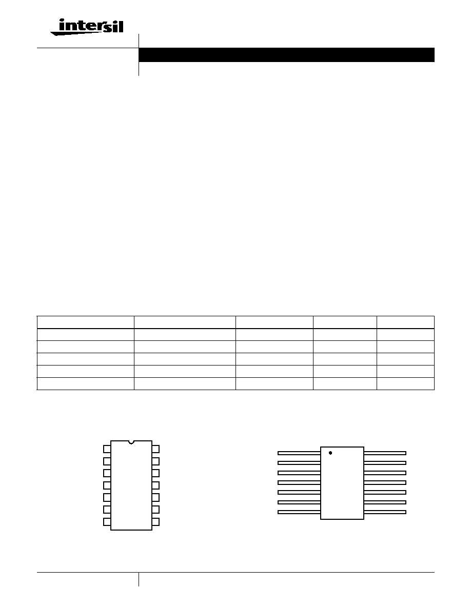
Pinouts
ACS32MS
(SBDIP)
TOP VIEW
ACS32MS
(FLATPACK)
TOP VIEW
A1
B1
Y1
A2
B2
Y2
GND
V
CC
B4
A4
Y4
B3
A3
Y3
1
2
3
4
5
6
7
14
13
12
11
10
9
8
14
13
12
11
10
9
8
2
3
4
5
6
7
1
A1
B1
Y1
A2
B2
Y2
GND
V
CC
B4
A4
Y4
B3
A3
Y3
Data Sheet
November 1998
File Number
4545
CAUTION: These devices are sensitive to electrostatic discharge; follow proper IC Handling Procedures.
1-888-INTERSIL or 321-724-7143 | Copyright © Intersil Corporation 1999
2
All Intersil semiconductor products are manufactured, assembled and tested under ISO9000 quality systems certification.
Intersil semiconductor products are sold by description only. Intersil Corporation reserves the right to make changes in circuit design and/or specifications at any time with-
out notice. Accordingly, the reader is cautioned to verify that data sheets are current before placing orders. Information furnished by Intersil is believed to be accurate and
reliable. However, no responsibility is assumed by Intersil or its subsidiaries for its use; nor for any infringements of patents or other rights of third parties which may result
from its use. No license is granted by implication or otherwise under any patent or patent rights of Intersil or its subsidiaries.
For information regarding Intersil Corporation and its products, see web site www.intersil.com
Sales Office Headquarters
NORTH AMERICA
Intersil Corporation
P. O. Box 883, Mail Stop 53-204
Melbourne, FL 32902
TEL: (321) 724-7000
FAX: (321) 724-7240
EUROPE
Intersil SA
Mercure Center
100, Rue de la Fusee
1130 Brussels, Belgium
TEL: (32) 2.724.2111
FAX: (32) 2.724.22.05
ASIA
Intersil (Taiwan) Ltd.
7F-6, No. 101 Fu Hsing North Road
Taipei, Taiwan
Republic of China
TEL: (886) 2 2716 9310
FAX: (886) 2 2715 3029
Die Characteristics
DIE DIMENSIONS:
Size: 2390
µ
m x 2390
µ
m (94 mils x 94 mils)
Thickness: 525
µ
m
±
25
µ
m (20.6 mils
±
1 mil)
Bond Pad: 110
µ
m x 110
µ
m (4.3 x 4.3 mils)
METALLIZATION: AL
Metal 1 Thickness: 0.7
µ
m
±
0.1
µ
m
Metal 2 Thickness: 1.0
µ
m
±
0.1
µ
m
SUBSTRATE POTENTIAL:
Unbiased Insulator
PASSIVATION
Type: Phosphorous Silicon Glass (PSG)
Thickness: 1.30
µ
m
±
0.15
µ
m
SPECIAL INSTRUCTIONS:
Bond V
CC
First
ADDITIONAL INFORMATION:
Worst Case Current Density: <2.0 x 10
5
A/cm
2
Transistor Count: 116
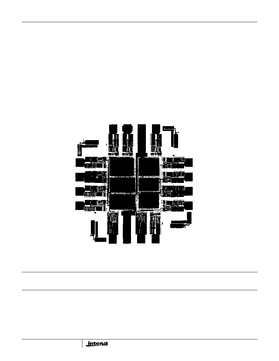
Metallization Mask Layout
ACS32MS
B1
A1
V
CC
B4
Y1 (3)
A2 (4)
NC
B2 (5)
(12) A4
(11) Y4
NC
(10) B3
(6)
(7)
(8)
(9)
A3
Y3
GND
Y2
(2)
(1)
(14)
(13)
ACS32MS