1
TM
File Number
4869.1
CAUTION: These devices are sensitive to electrostatic discharge; follow proper IC Handling Procedures.
1-888-INTERSIL or 321-724-7143
|
Intersil and Design is a trademark of Intersil Corporation.
|
Copyright
©
Intersil Corporation 2000
IS-2981RH
Radiation Hardened 8-Channel Source
Driver
The Star*Power Radiation Hardened
IS-2981RH is a monolithic device
designed for use in high-side
switching applications that benefit
from separate grounds for the logic and loads. The device
has a 5V to 80V operating supply voltage range and is
capable of sourcing -200mA continuously from each output.
The outputs are controlled by active-high inputs and may be
paralleled to increase the drive current. Output clamp diodes
prevent device damage, when switching inductive loads.
Constructed with the Intersil bonded wafer, dielectrically
isolated HVTDLM process, these single event latch-up
immune devices have been specifically designed to provide
highly reliable performance in harsh radiation environments.
They are fully guaranteed for 100krad(Si) total dose
performance through wafer-by-wafer radiation testing, and
are production tested over the full military temperature
range.
Specifications for Rad Hard QML devices are controlled
by the Defense Supply Center in Columbus (DSCC). The
SMD numbers listed here must be used when ordering.
Detailed Electrical Specifications for these devices are
contained in SMD 5962-00520. A "hot-link" is provided
on our homepage for downloading.
www.intersil.com/spacedefense/space.htm
Features
∑ Electrically Screened to SMD # 5962-00520
∑ QML Qualified Per MIL-PRF-38535 Requirements
∑ Radiation Environment
- Single Event Latch-up Immune. . . . . . . . . . . DI Process
- Total Dose . . . . . . . . . . . . . . . . . . . 1 x 10
5
rad(Si) (Max)
∑ Input Voltage Range . . . . . . . . . . . 0.0V to V
CC
(20V Max)
∑ Supply Voltage Range . . . . . . . . . . . . . . . . . . . . 5V to 80V
∑ Turn-on Delay Time . . . . . . . . . . . . . . . . . . . . . . 2
µ
s (Max)
∑ Turn-off Delay Time . . . . . . . . . . . . . . . . . . . . . 11
µ
s (Max)
∑ Output Clamp Diode, V
F
. . . . . . . . . . . . . . . -1.75V (Max)
Applications
∑ Drivers for Various Loads
- Relays, Solenoids and Motors
∑ Reliable Replacement of Discrete Solutions
∑ Interfacing Between Low-Level Logic and High-Current
Loads
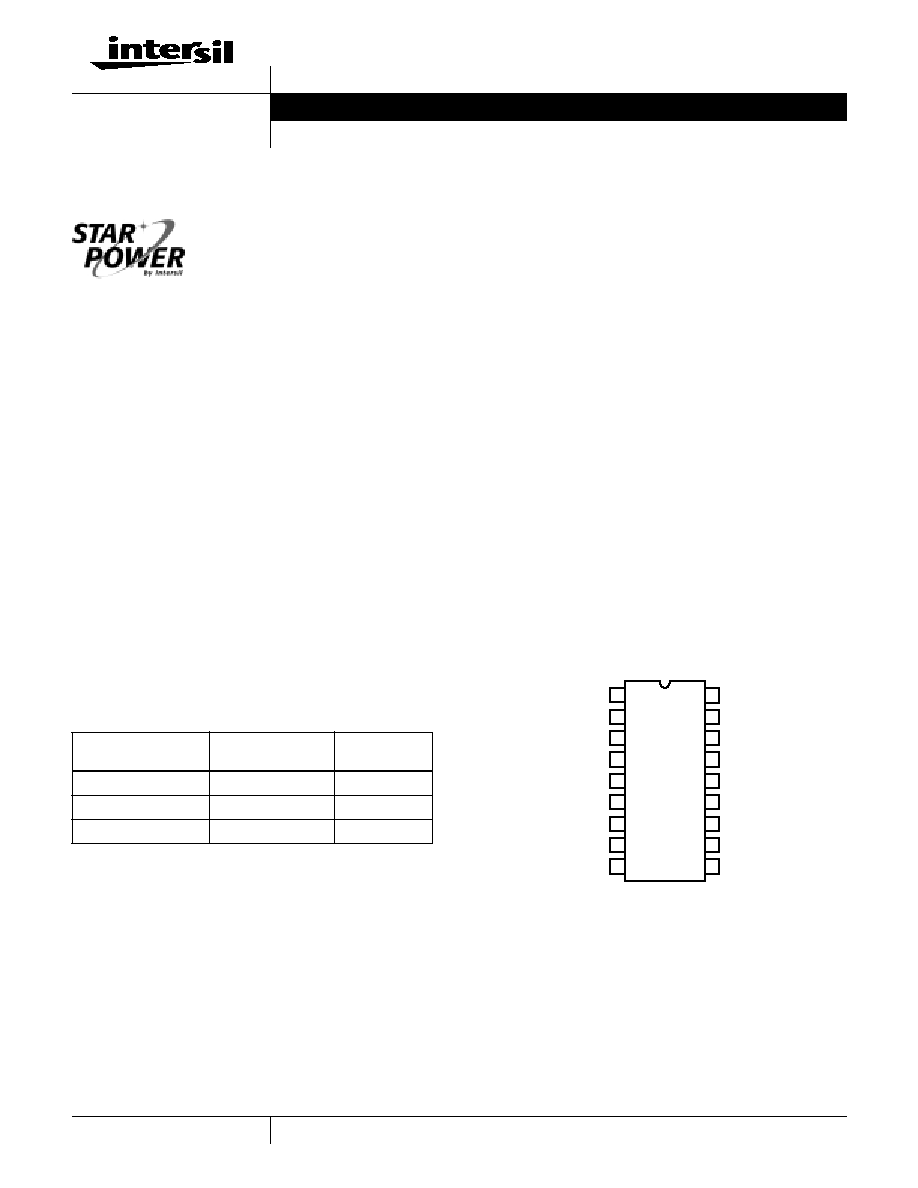
Pinout
IS1-2981RH-Q
(CDIP2-T18, SBDIP)
TOP VIEW
Ordering Information
ORDERING NUMBER
INTERNAL MKT.
NUMBER
TEMP. RANGE
(
o
C)
5962R0052001VVC
IS1-2981RH-Q
-55 to 125
5962R0052001QVC
IS1-2981RH-8
-55 to 125
IS1-2981RH/Proto
IS1-2981RH/Proto
-55 to 125
TM
10
11
12
13
14
15
16
17
18
9
8
7
6
5
4
3
2
1
OUT 1
OUT 3
OUT 4
OUT 5
OUT 6
OUT 7
OUT 8
OUT 2
GND
IN 1
IN 2
IN 3
IN 4
IN 5
IN 6
IN 8
IN 7
V
CC
Data Sheet
June 2000

2
All Intersil semiconductor products are manufactured, assembled and tested under ISO9000 quality systems certification.
Intersil semiconductor products are sold by description only. Intersil Corporation reserves the right to make changes in circuit design and/or specifications at any time with-
out notice. Accordingly, the reader is cautioned to verify that data sheets are current before placing orders. Information furnished by Intersil is believed to be accurate and
reliable. However, no responsibility is assumed by Intersil or its subsidiaries for its use; nor for any infringements of patents or other rights of third parties which may result
from its use. No license is granted by implication or otherwise under any patent or patent rights of Intersil or its subsidiaries.
For information regarding Intersil Corporation and its products, see web site www.intersil.com
Die Characteristics
DIE DIMENSIONS:
2667
µ
m x 5131
µ
m (105 mils x 202 mils)
Thickness: 483
µ
m
±
25.4
µ
m (19 mils
±
1 mil)
INTERFACE MATERIALS
Glassivation
Type: Nitride (Si
3
N
4
) over Silox (SiO
2
)
Nitride Thickness: 4.0k
≈
±
1.0k
≈
Silox Thickness: 12.0k
≈
±
4.0k
≈
Metallization
Top Metal 2: Ti/AlCu
Thickness: 1.6
µ
m
±
0.02
µ
m
Metal 1: Ti/AlCu
Thickness: 0.8
µ
m
±
0.01
µ
m
Substrate
HVTDLM, Bonded Wafer, Dielectric Isolation
Backside Finish
Silicon
ASSEMBLY RELATED INFORMATION
Substrate Potential
Must be tied to GND.
ADDITIONAL INFORMATION
Worst Case Current Density
<1.0 x 10
5
A/cm
2
Transistor Count
68
Metallization Mask Layout
IS-2981RH
8
7
6
5
4
3
2
1
9
9
10
11
12
13
14
15
16
17
18
10
10A
9
9
NOTES:
1. Pad numbers correspond to package pin functions.
2. Bond to all four pad 9 locations for V
CC
current sharing purposes.
3. Bond to both pad 10 locations for GND current sharing purposes.
4. Pad 10A is not used in die applications.
5. Die backside must be connected to GND.
IS-2981RH