
1
CAUTION: These devices are sensitive to electrostatic discharge; follow proper IC Handling Procedures.
http://www.intersil.com or 407-727-9207
|
Copyright
©
Intersil Corporation 1999
Ordering Information
PART NUMBER
TEMPERATURE RANGE
SCREENING LEVEL
PACKAGE
5962R9571401QRC
-55
o
C to +125
o
C
MIL-PRF-38535 Level Q
20 Lead SBDIP
5962R9571401QXC
-55
o
C to +125
o
C
MIL-PRF-38535 Level Q
20 Lead Ceramic Flatpack
5962R9571401VRC
-55
o
C to +125
o
C
MIL-PRF-38535 Level V
20 Lead SBDIP
5962R9571401VXC
-55
o
C to +125
o
C
MIL-PRF-38535 Level V
20 Lead Ceramic Flatpack
HS1-82C08RH/SAMPLE
+25
o
C
SAMPLE
20 Lead SBDIP
HS9-82C08RH/SAMPLE
+25
o
C
SAMPLE
20 Lead Ceramic Flatpack
HS-82C08RH
Radiation Hardened
8-Bit Bus Transceiver
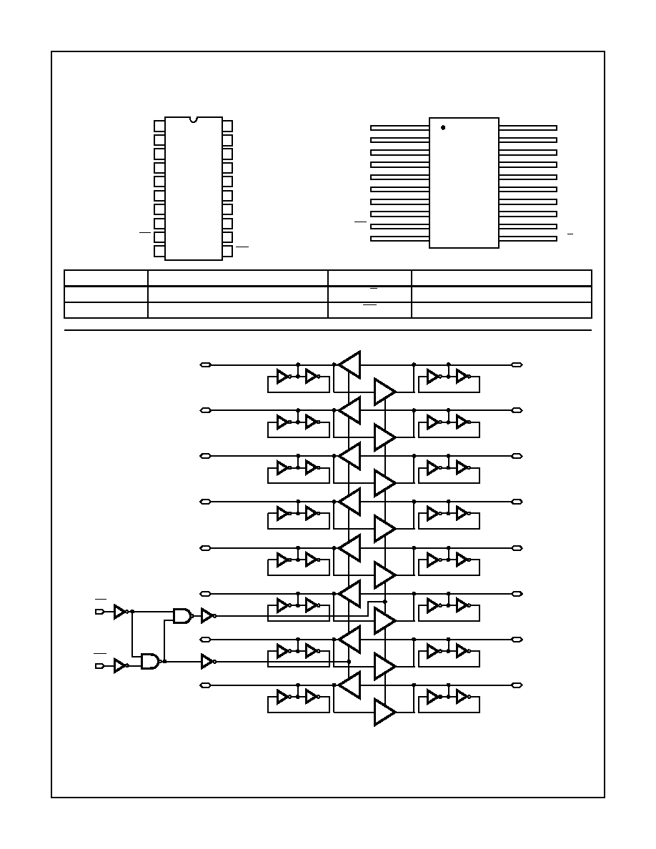
Functional Diagram
TRUTH TABLE
INPUTS
OPERATION
OUTPUT
ENABLE
TRANSMIT
/RECEIVE
PORT A
PORT B
0
0
Out
In
0
1
In
Out
1
X
High Z
High Z
X = Don't Care
A1
A2
A3
A4
A5
A6
A7
OE
PORT
A
A0
B1
B2
B3
B4
B5
B6
B7
PORT
B
B0
T/R
Features
∑ Devices QML Qualified in Accordance With
MIL-PRF-38535
∑ Detailed Electrical and Screening Requirements are
Contained in SMD# 5962-95714 and Intersil' QM Plan
∑ Radiation Hardened
- Total Dose 1 x 10
5
RAD (Si)
- Latch-Up Immune EPI-CMOS > 1 x 10
12
RAD (Si)/s
∑ Bidirectional Three-State Input/Outputs
∑ Low Propagation Delay Time
∑ Low Power Consumption
∑ Single Power Supply +5V
∑ Electrically Equivalent to Sandia SA2997
∑ Military Temperature Range -55
o
C to +125
o
C
Description
The Intersil HS-82C08RH is a radiation-hardened octal bus
transceiver with three-state outputs. It is manufactured using
a self-aligned, junction isolated CMOS process and is
designed for use with the HS-80C08RH radiation-hardened
microprocessor. The HS-82C08RH allows asynchronous
two-way communication between data buses. The direction
of data flow is determined by the logic level on the transmit/
receive (T/R) input. A logic high on the T/R input specifies
data flow from Port A to Port B of the device. Conversely, a
logic low on the T/R input specifies data flow from Port B to
Port A. The Output Enable input disables both ports by
placing them in the high impedance state.
The HS-82C08RH is ideally suited for a wide variety of
buffering applications in radiation-hardened microcomputer
systems.
February 1996
Spec Number
518057
File Number
3040.2
2
HS-82C08RH
Spec Number
518057
Logic Diagram
NOTE: An Important caveat that is applicable to CMOS devices in general is that unused inputs should never be left floating. This rule applies
to inputs connected to a three-state bus. The need for external pull-up resistors during three-state bus conditions is eliminated by the
presence of regenerative latches on the following HS-82C08RH pins. A0-7 and B0-7 The functional block diagram depicts one of
these pins with the regenerative latch. When the CMOS driver assumes the high impedance state, the latch holds the bus in whatever
logic state (high or low) it was before the three-state condition. A transient drive current of
±
1.5mA at VDD/2
±
0.5V for 10ns is required
to switch the latch. Thus, CMOS device inputs connected to the bus are not allowed to float during three-state conditions.
Pinouts
20 LEAD CERAMIC DUAL-IN-LINE
METAL-SEAL PACKAGE (SBDIP) MIL-STD-1835, CDIP2-T20
TOP VIEW
20 LEAD CERAMIC METAL SEAL
FLATPACK PACKAGE (FLATPACK) MIL-STD-1835, CDFP4-F20
TOP VIEW
PIN
DESCRIPTION
PIN
DESCRIPTION
A0-A7
Local Bus Data I/O Pins
T/R
Transmit/Receive Input
B0-B7
System Bus Data I/O Pins
OE
Active Low Output Enable
11
12
13
14
15
16
17
18
20
19
10
9
8
7
6
5
4
3
2
1
A0
A1
A2
A3
A4
A5
A7
A6
OE
GND
VDD
B1
B2
B3
B0
B4
B5
B6
B7
T/R
2
3
4
5
6
7
8
1
20
19
18
17
16
15
14
13
A0
A1
A2
A3
A4
A5
A6
A7
9
10
12
11
OE
GND
VDD
B0
B1
B2
B3
B4
B5
B6
B7
T/R
1
A0
TSB
TSB
B ENABLE
19
B0
2
A1
TSB
TSB
18
B1
3
A2
TSB
TSB
17
B2
4
A3
TSB
TSB
16
B3
5
A4
TSB
TSB
15
B4
6
A5
TSB
TSB
14
B5
7
A6
TSB
TSB
13
B6
8
A7
TSB
TSB
12
B7
A ENABLE
OE 9
T/R11
3
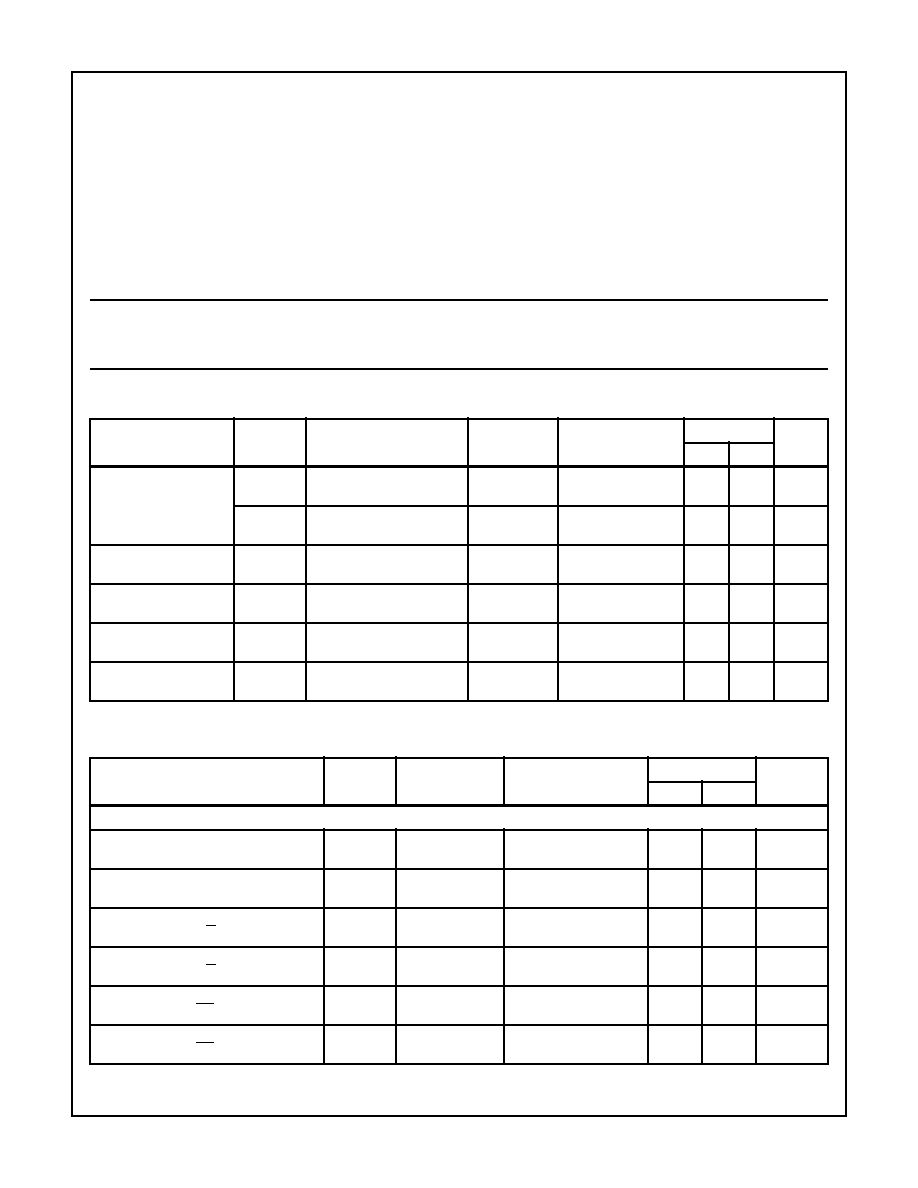
Specifications HS-82C08RH
Absolute Maximum Ratings
Reliability Information
Supply Voltage . . . . . . . . . . . . . . . . . . . . . . . . . . . . . . . . . . . . . +7.0V
Input, Output or I/O Voltage . . . . . . . . . . . . GND-0.3V to VDD+0.3V
Storage Temperature Range . . . . . . . . . . . . . . . . . -65
o
C to +150
o
C
Junction Temperature . . . . . . . . . . . . . . . . . . . . . . . . . . . . . . +175
o
C
Lead Temperature (Soldering 10s) . . . . . . . . . . . . . . . . . . . . +300
o
C
ESD Classification . . . . . . . . . . . . . . . . . . . . . . . . . . . . . . . . Class 1
Thermal Resistance
JA
JC
20 Lead SBDIP Package. . . . . . . . . . . . .
71
o
C/W
17
o
C/W
20 Lead Ceramic Flatpack Package . . . .
85
o
C/W
25
o
C/W
Maximum Package Power Dissipation at +125
o
C Ambient
20 Lead SBDIP Package. . . . . . . . . . . . . . . . . . . . . . . . . . . 0.70W
20 Lead Ceramic Flatpack Package . . . . . . . . . . . . . . . . . . 0.59W
If device power exceeds package dissipation capability, provide heat
sinking or derate linearly at the following rate:
20 Lead SBDIP Package. . . . . . . . . . . . . . . . . . . . . . . .14.1mW/C
20 Lead Ceramic Flatpack Package . . . . . . . . . . . . . . . 11.8mW/C
CAUTION: Stresses above those listed in "Absolute Maximum Ratings" may cause permanent damage to the device. This is a stress only rating and operation
of the device at these or any other conditions above those indicated in the operational sections of this specification is not implied.
Operating Conditions
Operating Voltage Range . . . . . . . . . . . . . . . . . . . +4.75V to +5.25V
Operating Temperature Range . . . . . . . . . . . . . . . . -55
o
C to +125
o
C
Input Low Voltage . . . . . . . . . . . . . . . . . . . . . . . . . . . . . . . 0V to +1V
Input High Voltage. . . . . . . . . . . . . . . . . . . . . . . . . . VDD -1V to VDD
TABLE 1. DC ELECTRICAL PERFORMANCE CHARACTERISTICS
All Devices Guaranteed at Worst Case Limits and Conditions.
PARAMETER
SYMBOL
CONDITIONS
GROUP A
SUBGROUPS
TEMPERATURE
LIMITS
UNITS
MIN
MAX
Input Leakage Current
IIL
VDD = 5.25V, VIN = VDD
Pin Under Test = 0V
1, 2, 3
-55
o
C, +25
o
C,
+125
o
C
-1.0
-
µ
A
IIH
VDD = 5.25V, VIN = 0V
Pin Under Test = 5.25V
1, 2, 3
-55
o
C, +25
o
C,
+125
o
C
-
1.0
µ
A
High Level Output
Voltage
VOH
VDD = 4.75V, IOH = -2.0mA
1, 2, 3
-55
o
C, +25
o
C,
+125
o
C
4.25
-
V
Low Level Output
Voltage
VOL
VDD = 5.25V, IOL = 2.0mA
1, 2, 3
-55
o
C, +25
o
C,
+125
o
C
-
0.5
V
Static Current
SIDD
VDD = 5.25V, VIN = GND
1, 2, 3
-55
o
C, +25
o
C,
+125
o
C
-
100
µ
A
Functional Test
FT
VDD = 4.75V to 5.25V
VIH = VDD -1.0V, VIL = 1.0V
7, 8A, 8B
-55
o
C, +25
o
C,
+125
o
C
-
-
-
TABLE 2. AC ELECTRICAL PERFORMANCE CHARACTERISTICS
PARAMETER
SYMBOL
GROUP A
SUBGROUPS
TEMPERATURE
LIMITS
UNITS
MIN
MAX
PORT DATA/MODE SPECIFICATIONS
Propagation Delay to Logical "1" from Port
A, B to Port B, A
TPDLH
9, 10, 11
-55
o
C, +25
o
C, +125
o
C
-
65
ns
Propagation Delay to Logical "0" from Port
A, B to Port B, A
TPDHL
9, 10, 11
-55
o
C, +25
o
C, +125
o
C
-
80
ns
Propagation Delay from High-Impedance
to Logical "1" from T/R to Port
TPRTH
9, 10, 11
-55
o
C, +25
o
C, +125
o
C
-
75
ns
Propagation Delay from High-Impedance
to Logical "0" from T/R to Port
TPRTL
9, 10, 11
-55
o
C, +25
o
C, +125
o
C
-
130
ns
Propagation Delay from High-Impedance
to Logical "1" from OE to Port
TPZH
9, 10, 11
-55
o
C, +25
o
C, +125
o
C
-
70
ns
Propagation Delay from High-Impedance
to Logical "0" from OE to Port
TPZL
9, 10, 11
-55
o
C, +25
o
C, +125
o
C
-
130
ns
Spec Number
518057

4
Specifications HS-82C08RH
TABLE 3. ELECTRICAL PERFORMANCE CHARACTERISTICS
PARAMETER
SYMBOL
(NOTE)
CONDITIONS
TEMPERATURE
LIMITS
UNITS
MIN
MAX
In/Out Capacitance
CI/O
VDD = Open, f = 1MHz
All Measurements Referenced
to GND.
+25
o
C
-
10
pF
TRANSMIT/RECEIVE MODE SPECIFICATIONS (AC Parameters)
Propagation Delay from Logical "1" to
High-Impedance from T/R to Port
TPHZTR
+25
o
C
-
35
ns
Propagation Delay from Logical "0" to
High-Impedance from T/R to Port
TPLZTR
+25
o
C
-
35
ns
Propagation Delay from Logical "1" to
High-Impedance from OE to Port
TPHZ
+25
o
C
-
35
ns
Propagation Delay from Logical "0" to
High-Impedance from OE to Port
TPLZ
+25
o
C
-
35
ns
NOTE:
1. The parameters listed are controlled via design or process parameters and are not directly tested. These parameters are characterized
upon initial design release and upon design changes which could affect these characteristics.
TABLE 4. POST 100K RAD ELECTRICAL PERFORMANCE CHARACTERISTICS
NOTE:
The Post Irradiation test conditions and limits are the same as those listed in Table 1 and Table 2.
TABLE 5. BURN-IN DELTA PARAMETERS (+25
o
C; In Accordance With SMD)
Switching Time Waveforms
FIGURE 1. PORT TO PORT
FIGURE 2. AC TESTING LOAD CIRCUIT
FIGURE 3. OE TO HIGH-IMPEDANCE, OE TO PORT OUTPUT
INPUT
AN OR BN
OUTPUT
BN OR AN
VDD
0V
VDD
0V
0.5VDD
tPLH
tPHL
0.5VDD
TR
TF
0.5VDD
0.5VDD
TR = TF
20ns
10% to 90%
DEVICE
UNDER
TEST
TEST POINTS
CL (NOTE)
NOTE: CL includes stray and jig capacitance.
0.5VDD
0.5VDD
0.5VDD
0.5VDD
tPHZ
tPLZ
0.1VDD
0.1VDD
VDD
0V
VOH
VOL
INPUT OE
PORT
OUTPUT
PORT
OUTPUT
TR
TF
tPZH
tPZL
0V
VDD
TR = TF
20ns
10% to 90%
Spec Number
518057

5
HS-82C08RH
Metallization Topology
DIE DIMENSIONS:
76.0 mils x 89.4 mils x 14 mils
±
1 mil
METALLIZATION:
Type: Si - Al
Thickness: 11k
≈
±
2k
≈
GLASSIVATION:
Type: SiO
2
Thickness: 8k
≈
±
1k
≈
Metallization Mask Layout
HS-82C08RH
A1 (2)
A2 (3)
A3 (4)
A4 (5)
A5 (6)
A6 (7)
A7 (8)
(12) B7
(13) B6
(14) B5
(15) B4
(16) B3
(17) B2
(18) B1
OE (9)
GND (10)
T/
R (9)
(19) B0
(20) VDD
(1) A0
Spec Number
518057