1
CAUTION: These devices are sensitive to electrostatic discharge; follow proper IC Handling Procedures.
www.intersil.com or 407-727-9207
|
Copyright
©
Intersil Corporation 1999
Satellite Applications FlowTM (SAF) is a trademark of Intersil Corporation.
CD4049UBT
CMOS Hex Buffer/Converter
Intersil's Satellite Applications Flow
TM
(SAF) devices are fully
tested and guaranteed to 100kRAD total dose. These QML
Class T devices are processed to a standard flow intended
to meet the cost and shorter lead-time needs of large
volume satellite manufacturers, while maintaining a high
level of reliability.
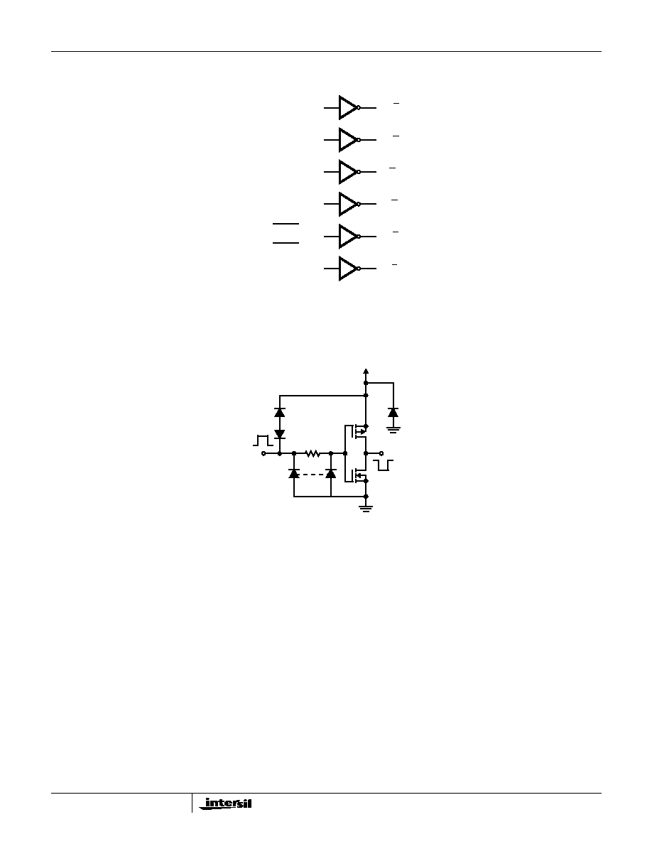
The CD4049UBT is an Inverting Hex Buffer and features
logic level conversion using only one supply (voltage (V
CC
).
The input signal high level (V
IH
) can exceed the V
CC
supply
voltage when this device is used for logic level conversions.
This device is intended for use as CMOS to DTL/TTL
converters and can drive directly two DTL/TTL loads. (V
CC
=
5V, V
OL
0.4V, and I
OL
3.3mA.
The CD4049UBT is the designated replacement for the
CD4009UB. Because the CD4049UBT requires only one
power supply, it is preferred over the CD4009UB and
CD4010B and should be used in place of the CD4009UB in
all inverter, current driver, or logic level conversion
applications. In these applications the CD4049UBT is pin
compatible with the CD4009UB, and can be substituted for
this device in existing as well as in new designs. Terminal
No. 16 is not connected internally on the CD4049UBT,
therefore, connection to this terminal is of no consequence
to circuit operation. For applications not requiring high sink
current or voltage conversion, the CD4069UB Hex Inverter is
recommended.
Specifications
Specifications for Rad Hard QML devices are controlled by
the Defense Supply Center in Columbus (DSCC). The SMD
numbers listed below must be used when ordering.
Detailed Electrical Specifications for the CD4049UBT are
contained in SMD 5962-96636. A "hot-link" is provided from
our website for downloading.
www.intersil.com/spacedefense/newsafclasst.asp
Intersil's Quality Management Plan (QM Plan), listing all
Class T screening operations, is also available on our web-
site.
www.intersil.com/quality/manuals.asp
Features
∑ QML Class T, Per MIL-PRF-38535
∑ Radiation Performance
- Gamma Dose (
) 1 x 10
5
RAD(Si)
- SEP Effective LET >75 MEV-gm/cm
2
∑ Inverting Type
∑ High Sink Current for Driving 2 TTL Loads
∑ High-to-Low Level Logic Conversion
∑ 100% Tested for Quiescent Current at 20V
∑ 5V, 10V and 15V Parametric Ratings
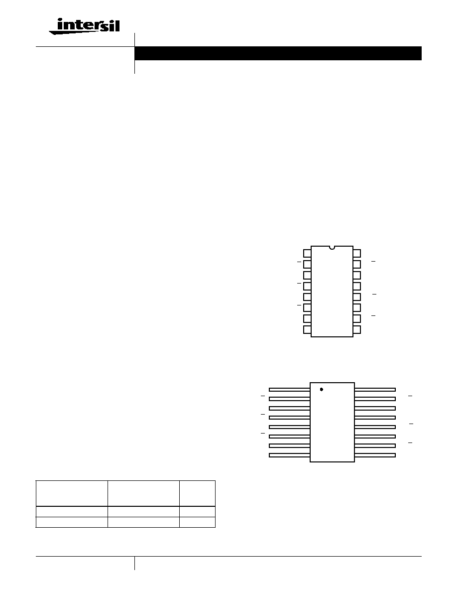
Pinouts
CD4049BT (SBDIP), CDIP2-T16
TOP VIEW
CD4049BT (FLATPACK), CDFP4-F16
TOP VIEW
Ordering Information
ORDERING
NUMBER
PART
NUMBER
TEMP.
RANGE
(
o
C)
5962R9663601TEC
CD4049UBDTR
-55 to 125
5962R9663601TXC
CD4049UBKTR
-55 to 125
NOTE:
Minimum order quantity for -T is 150 units through
distribution, or 450 units direct.
14
15
16
9
13
12
11
10
1
2
3
4
5
7
6
8
V
CC
G = A
A
H = B
B
I = C
V
SS
C
NC
F
NC
K = E
E
J = D
D
L = F
V
CC
G = A
A
H = B
B
I = C
C
V
SS
2
3
4
5
6
7
8
1
16
15
14
13
12
11
10
9
NC
L = F
F
NC
K = E
E
J = D
D
Data Sheet
July 1999
File Number
4622.1
3
All Intersil semiconductor products are manufactured, assembled and tested under ISO9000 quality systems certification.
Intersil semiconductor products are sold by description only. Intersil Corporation reserves the right to make changes in circuit design and/or specifications at any time with-
out notice. Accordingly, the reader is cautioned to verify that data sheets are current before placing orders. Information furnished by Intersil is believed to be accurate and
reliable. However, no responsibility is assumed by Intersil or its subsidiaries for its use; nor for any infringements of patents or other rights of third parties which may result
from its use. No license is granted by implication or otherwise under any patent or patent rights of Intersil or its subsidiaries.
For information regarding Intersil Corporation and its products, see web site http://www.intersil.com
Sales Office Headquarters
NORTH AMERICA
Intersil Corporation
P. O. Box 883, Mail Stop 53-204
Melbourne, FL 32902
TEL: (407) 724-7000
FAX: (407) 724-7240
EUROPE
Intersil SA
Mercure Center
100, Rue de la Fusee
1130 Brussels, Belgium
TEL: (32) 2.724.2111
FAX: (32) 2.724.22.05
ASIA
Intersil (Taiwan) Ltd.
7F-6, No. 101 Fu Hsing North Road
Taipei, Taiwan
Republic of China
TEL: (886) 2 2716 9310
FAX: (886) 2 2715 3029
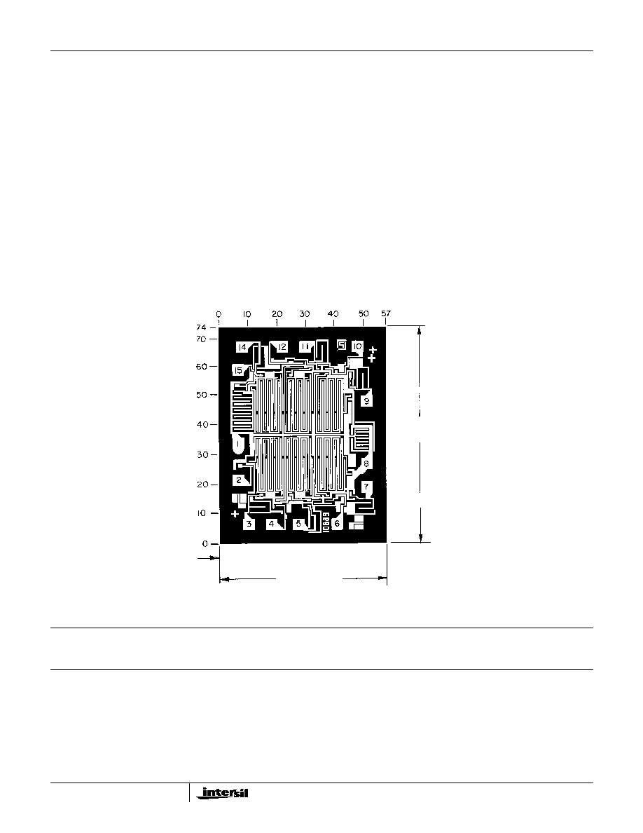
Die Characteristics
DIE DIMENSIONS:
(1448
µ
m x 1880
µ
m x 533
µ
m
±
25.4
µ
m)
57 x 74 x 21mils
±
1mil
METALLIZATION:
Type: Al
Thickness: 12.5k
≈
±
1.5k
≈
SUBSTRATE POTENTIAL:
Leave Floating or Tie to V
CC
Bond Pad #1 (V
CC
) First
BACKSIDE FINISH:
Silicon
PASSIVATION:
Type: Phosphorus Doped Silox (S
i
O
2
)
Thickness: 13.0k
≈
±
2.6k
≈
WORST CASE CURRENT DENSITY:
< 2.0e5 A/cm
2
TRANSISTOR COUNT:
12
PROCESS:
Bulk CMOS
Metallization Mask Layout
CD4049UBT
74mils
57mils
CD4049UBT