1
Æ
CAUTION: These devices are sensitive to electrostatic discharge; follow proper IC Handling Procedures.
1-888-INTERSIL or 321-724-7143
|
Intersil (and design) is a registered trademark of Intersil Americas Inc.
Copyright © Intersil Americas Inc. 2003. All Rights Reserved
All other trademarks mentioned are the property of their respective owners.
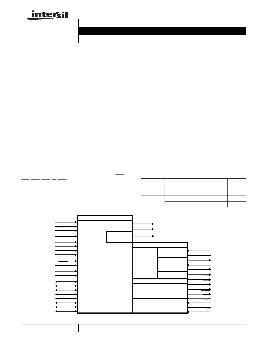
CMOS Asynchronous
The 82C50A Asynchronous Communication Element
(ACE) is a high performance programmable Universal
Asynchronous Receiver/Transmitter (UART) and Baud
Rate Generator (BRG) on a single chip. Using Intersil's
advanced Scaled SAJI IV CMOS Process, the ACE will
support data rates from DC to 625K baud (0-10MHz clock).
The ACE's receiver circuitry converts start, data, stop, and
parity bits into a parallel data word. The transmitter circuitry
converts a parallel data word into serial form and appends
the start, parity, and stop bits. The word length is
programmable to 5, 6, 7, or 8 data bits. Stop bit selection
provides a choice of 1,1.5, or 2 stop bits.
The Baud Rate Generator divides the clock by a divisor
programmable from 1 to 2
16
-1 to provide standard RS-
232C baud rates when using any one of three industry
standard baud rate crystals (1.8432MHz, 2.4576MHz, or
3.072MHz). A programmable buffered clock output
(BAUDOUT) provides either a buffered oscillator or 16X (16
times the data rate) baud rate clock for general purpose
system use.
To meet the system requirements of a CPU interfacing to
an asynchronous channel, the modem control signals RTS,
CTS, DSR, DTR, RI, DCD are provided. Inputs and outputs
have been designed with full TTL/CMOS compatibility in
order to facilitate mixed TTL/NMOS/CMOS system design.
Features
∑ Single Chip UART/BRG
∑ DC to 625K Baud (DC to 10MHz Clock)
∑ Crystal or External Clock Input
∑ On Chip Baud Rate Generator 1 to 65535 Divisor
Generates 16X Clock
∑ Prioritized Interrupt Mode
∑ Fully TTL/CMOS Compatible
∑ Microprocessor Bus Oriented Interface
∑ 80C86/80C88 Compatible
∑ Scaled SAJI IV CMOS Process
∑ Low Power - 1mA/MHz Typical
∑ Modem Interface
∑ Line Break Generation and Detection
∑ Loopback and Echo Modes
∑ Doubled Buffered Transmitter and Receiver
∑ Single 5V Supply
Functional Diagram
Ordering Information
PACKAGE
TEMPERATURE
RANGE (
o
C)
625K BAUD
PKG.
DWG. #
PDIP
0 to +70
CP82C50A-5
E40.6
PLCC
0 to +70
CS82C50A-596
N44.65
-40 to +85
IS82C50A-5
N44.65
D0
D1
D2
D3
D4
D5
D6
D7
1
2
3
4
5
6
7
8
A0
A1
A2
MR
DISTR
DISTR
DOSTR
DOSTR
28
27
26
35
22
21
19
18
CSO
CS1
CS2
12
13
14
ADS
25
MICROPROCESSOR INTERFACE
INTERRUPT
ENABLE,
ID, & CONTROL
30 INTRPT
23
DDIS
24 CSOUT
10
SIN
UART
MODEM
DIVISOR LATCH
AND BAUD RATE
GENERATOR
MODEM CONTROL
MODEM STATUS
RECEIVER
TRANSMITTER
9
RCLK
16
XTAL1
15 BAUDOUT
17
XTAL2
11
SOUT
32
RTS
33
DTR
34
OUT1
31
OUT2
36
CTS
37
DSR
38
DCD
39
RI
LINE STATUS
AND CONTROL
FN2958.2
82C50A
Data Sheet
May 2003
2
82C50A
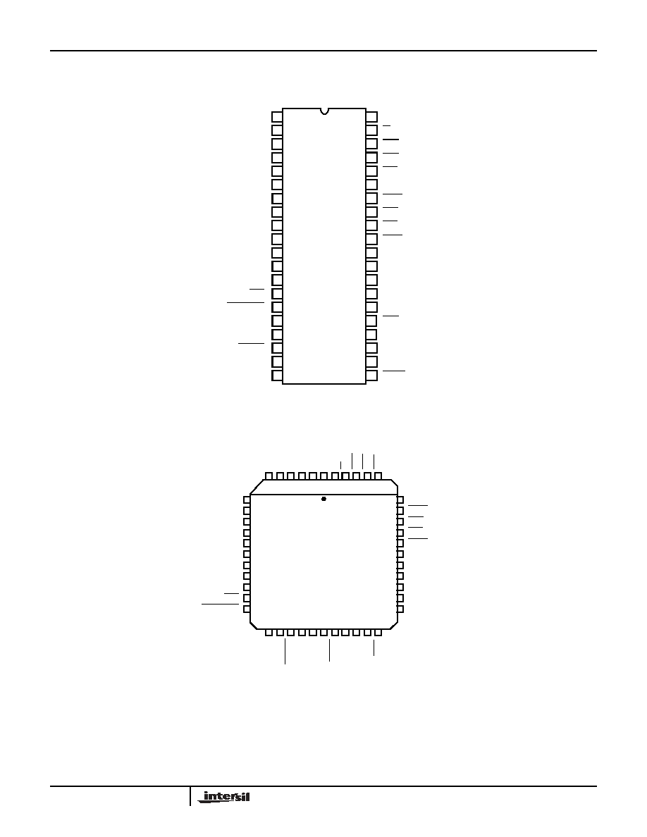
Pinout
82C50A (PDIP)
TOP VIEW
82C50A (PLCC)
TOP VIEW
13
1
2
3
4
5
6
7
8
9
10
11
12
14
15
16
17
18
19
20
D0
D1
D2
D3
D4
D5
D6
D7
RCLK
SIN
SOUT
CS0
CS1
CS2
BAUDOUT
XTAL1
XTAL2
DOSTR
DOSTR
GND
28
40
39
38
37
36
35
34
33
32
31
30
29
27
26
25
24
23
22
21
V
CC
RI
DCD
DSR
CTS
MR
OUT1
DTR
RTS
OUT2
INTRPT
NC
A0
A1
A2
ADS
CSOUT
DDIS
DISTR
DISTR
44 43 42 41 40
39
38
37
36
35
34
33
32
31
30
29
28
27
1
2
3
4
5
6
20 21 22 23 24 25 26
19
18
7
8
9
10
11
12
13
14
15
16
17
D5
D6
D7
RCLK
SIN
NC
SOUT
CS0
CS1
CS2
BAUDOUT
D4
D3
D2
D1
D0
NC
V
CC
RI
DCD
DSR
CTS
XTA
L
1
XTA
L
2
DOSTR
DOSTR
GND
NC
DIS
T
R
DIS
T
R
DD
I
S
CSOUT
ADS
MR
OUT1
DTR
RTS
OUT2
NC
INTRP
NC
A0
A1
A2
3
82C50A
Pin Description
SYMBOL
PIN
NUMBER
TYPE
ACTIVE
LEVEL
DESCRIPTION
DISTR,
DISTR
22
21
I
I
H
L
DATA IN STROBE, DATA IN STROBE: DISTR, DISTR are read inputs which cause the
82C50A to output data to the data bus (D0-D7). The data output depends upon the
register selected by the address inputs A0, A1, A2. The chip select inputs CS0, CS1,
CS2 enable the DISTR, DISTR inputs.
Only an active DISTR or DISTR, not both, is used to receive data from the 82C50A
during a read operation. If DISTR is used as the read input, DlSTR should be tied high.
If DISTR is used as the active read input, DISTR should be tied low.
DOSTR,
DOSTR
19
18
I
I
H
L
DATA OUT STROBE, DATA OUT STROBE: DOSTR, DOSTR are write inputs which
cause data from the data bus (D0-D7) to be input to the 82C50A. The data input depends
upon the register selected by the address inputs A0, A1, A2. The chip select inputs CS0,
CS1, CS2 enable the DOSTR, DOSTR inputs.
Only an active DOSTR or DOSTR, not both, is used to transmit data to the 82C50A
during a write operation. If DOSTR is used as the write input, DOSTR should be tied
high. If DOSTR is used as the write input, DOSTR should be tied low.
D0-D7
1-8
I/O
DATA BITS 0-7: The Data Bus provides eight, three-state input/output lines for the
transfer of data, control and status information between the 82C50A and the CPU. For
character formats of less than 8 bits, D7, D6 and D5 are "don't cares" for data write
operations and 0 for data read operations. These lines are normally in a high impedance
state except during read operations. D0 is the Least Significant Bit (LSB) and is the first
serial data bit to be received or transmitted.
A0, A1,
A2
28, 27,
26
I
I
H
REGISTER SELECT: The address lines select the internal registers during CPU bus
operations. See Table 1.
XTAL1,
XTAL2
16
17
I
O
CRYSTAL/CLOCK: Crystal connections for the internal Baud Rate Generator. XTAL1
can also be used as an external clock input, in which case XTAL2 should be left open.
SOUT
11
O
SERIAL DATA OUTPUT: Serial data output from the 82C50A transmitter circuitry. A
Mark (1) is a logic one (high) and Space (0) is a logic zero (low). SOUT is held in the
Mark condition when the transmitter is disabled, MR is true, the Transmitter Register is
empty, or when in the Loop Mode. SOUT is not affected by the CTS input.
GND
20
L
GROUND: Power supply ground connection (V
SS
).
CTS
36
I
L
CLEAR TO SEND: The logical state of the CTS pin is reflected in the CTS bit of the
(MSR) Modem Status Register (CTS is bit 4 of the MSR, written MSR (4)). A change of
state in the CTS pin since the previous reading of the MSR causes the setting of DCTS
(MSR(O)) of the Modem Status Register. When CTS pin is ACTIVE (low), the modem is
indicating that data on SOUT can be transmitted on the communications link. If CTS pin
goes INACTIVE (high), the 82C50A should not be allowed to transmit data out of SOUT.
CTS pin does not affect Loop Mode operation.
DSR
37
I
L
DATA SET READY: The logical state of the DSR pin is reflected in MSR(5) of the
Modem Status Register. DDSR (MSR(1)) indicates whether the DSR pin has changed
state since the previous reading of the MSR. When the DSR pin is ACTIVE (low), the
modem is indicating that it is ready to exchange data with the 82C50A, while the DSR
Pin INACTIVE (high) indicates that the modem is not ready for data exchange. The
ACTIVE condition indicates only the condition of the local Data Communications
Equipment (DCE), and does not imply that a data circuit as been established with remote
equipment.
DTR
33
O
L
DATA TERMINAL READY: The DTR pin can be set (low) by writing a logic 1 to MCR(0),
Modem Control Register bit 0. This signal is cleared (high) by writing a logic 0 to the DTR
bit (MCR(0)) or whenever a MR ACTIVE (high) is applied to the 82C50A. When ACTIVE
(low), DTR pin indicates to the DCE that the 82C50A is ready to receive data. In some
instances, DTR pin is used as a power on indicator. The INACTIVE (high) state causes
the DCE to disconnect the modem from the telecommunications circuit.
RTS
32
O
L
REQUEST TO SEND: The RTS signal is an output used to enable the modem. The RTS
pin is set low by writing a logic 1 to MCR (1) bit 1 of the Modem Control Register. The
RTS pin is reset high by Master Reset. When ACTIVE, the RTS pin indicates to the DCE
that the 82C50A has data ready to transmit. In half duplex operations, RTS is used to
control the direction of the line.
BAUDOUT
15
O
BAUDOUT: This output is a 16X clock out used for the transmitter section (16X = 16
times the data rate). The BAUDOUT clock rate is equal to the reference oscillator
frequency divided by the specified divisor in the Baud Rate Generator Divisor Latches
DLL and DLM. BAUDOUT may be used by the Receiver section by tying this output to
RCLK.
4
82C50A
OUT1
34
O
L
OUTPUT 1: This is a general purpose output that can be programmed ACTIVE (low) by
settingVCR(2) (OUT1) of the Modem Control Register to a high level. The OUT1 pin is
set high by Master Reset. The OUT1 pin is INACTIVE (high) during loop mode operation.
OUT2
31
O
L
OUTPUT 2: This is a general purpose output that can be programmed ACTIVE (low) by
setting MCR(3) (OUT1) of the Modem Control Register to a high level. The OUT2 pin is
set high by Master Reset. The OUT2 signal is INACTIVE (high) during loop mode
operation.
RI
39
1
L
RING INDICATOR: When low, RI indicates that a telephone ringing signal has been
received by the modem or data set. The RI signal is a modem control input whose
condition is tested by reading MSR(6) (RI). The Modem Status Register output TERI
(MSR(2)) indicates whether the RI input has changed from a Low to High since the
previous reading of the MSR. If the interrupt is enabled (IER (3) = 1) and RI changes from
a Low to High, an interrupt is generated. The ACTIVE (low) state of RI indicates that the
DCE is receiving a ringing signal. RI will appear ACTIVE for approximately the same
length of time as the ACTIVE segment of the ringing cycle. The INACTIVE state of RI
will occur during the INACTIVE segments not detected by the DCE. This circuit is not
disabled by the INACTIVE condition of DTR.
DCD
38
I
L
DATA CARRIER DETECT: When ACTIVE (low), DCD indicates that the data carrier
has been detected by the modem or data set. DCD is a modem input whose condition
can be tested by the CPU by reading MSR(7) (DCD) of the Modem Status Register.
MSR(3) (DDCD) of the Modem Status Register indicates whether the DCD input has
changed since the previous reading of the MSR. DOD has no effect on the receiver. If
the DCD changes state with the modem status interrupt enabled, an interrupt is
generated.
When DCD is ACTIVE (low), the received line signal from the remote terminal is within
the limits specified by the DCE manufacturer. The INACTIVE (high) signal indicates that
the signal is not within the specified limits, or is not present.
MR
35
1
H
MASTER RESET: The MR input forces the 82C50A into an idle mode in which all serial
data activities are suspended. The Modem Control Register (MCR) along with its
associated outputs are cleared. The Line Status Register (LSR) is cleared except for the
THRE and TEMT bits, which are set. The 82C50A remains in an idle state until
programmed to resume serial data activities. The MR input is a Schmitt trigger input. See
the DC Electrical Characteristics for Schmitt trigger logic input voltage levels. See Table
7 for a summary of Master Reset's effect on 82C50A operation.
lNTRPT
30
O
H
INTERRUPT REQUEST: The lNTRPT output goes ACTIVE (high) when one of the
following interrupts has an ACTIVE (high) condition and is enabled by the Interrupt
Enable Register: Receiver Error flag, Received Data Available, Transmitter Holding
Register Empty, and Modem Status. The lNTRPT is reset low upon appropriate service
or a MR operation. See Figure 1. Interrupt Control Structure.
SIN
10
I
H
SERIAL DATA INPUT: The SIN input is the serial data input from the communication
line or modem to the 82C50A receiver circuits. A mark (1) is high, and a space (0) is low.
Data inputs on SIN are disabled when operating in the loop mode.
V
CC
40
H
V
CC
: +5V positive power supply pin. A 0.1
µ
A decoupling capacitor from V
CC
(pin 40)
to GND (pin 20) is recommended.
CS0, CS1,
CS2
12,13,
14
I
I
H, H,
L
CHIP SELECT: The Chip Select inputs act as enable signals for the write (DOSTR,
DOSTR) and read (DlSTR, DlSTR) input signals. The Chip Select inputs are latched by
the ADS input.
NC
29
Do Not Connect
CSOUT
24
O
H
CHIP SELECT OUT: When ACTIVE (high), this pin indicates that the chip has been
selected by active CS0, CS1, and CS2 inputs. No data transfer can be initiated until
CSOUT is a logic 1, ACTIVE (high).
DDIS
23
O
H
DRIVER DISABLE: This output is INACTIVE (low) when the CPU is reading data from
the 82C50A. An ACTIVE (high) Dells output can be used to disable an external
transceiver when the CPU is reading data.
ADS
25
I
L
ADDRESS STROBE: When ACTIVE (low), ADS latches the Register Select (A0, A1,
A2) and Chip Select (CS0, CS1, CS2) inputs. An active ADS is required when the
Register Select pins are not stable for the duration of the read or write operation,
multiplexed mode. If not required, the ADS input should be tied low, non-multiplexed
mode.
RCLK
9
I
This input is the 16X Baud Rate Clock for the receiver section of the 82C50A. This input
may be provided from the BAUDOUT output or an external clock.
Pin Description
(Continued)
SYMBOL
PIN
NUMBER
TYPE
ACTIVE
LEVEL
DESCRIPTION
5
82C50A
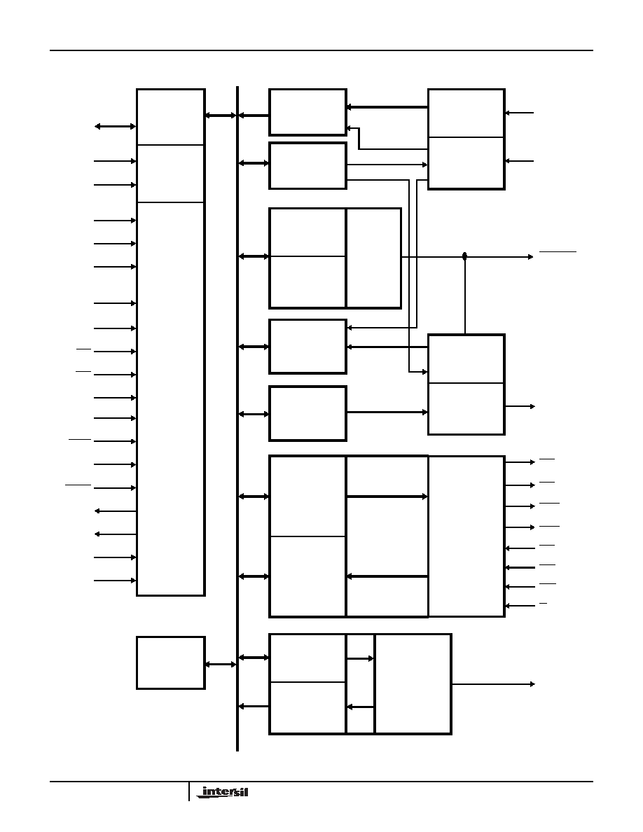
Block Diagram
DISTR
DISTR
DOSTR
DOSTR
DDIS
CSOUT
XTAL1
XTAL2
(22)
(21)
(19)
(18)
(23)
(24)
(16)
(17)
A0
A1
A2
CS0
CS1
CS2
ADS
MR
(28)
(27)
(26)
(12)
(13)
(14)
(25)
(35)
D7 - D0
(1 - 8)
(40)
(20)
DATA BUS
RECEIVER SHIFT
BUFFER
POWER
SUPPLY
SELECT
&
CONTROL
LOGIC
(10)
SIN
(9)
RCLK
(15)
BAUDOUT
(11)
SOUT
(32)
RTS
(33)
DTR
(34)
OUT1
(36)
OUT2
(31)
CTS
(37)
DSR
(38)
DCD
(39)
RI
RECEIVER
RECEIVER TIMING
& CONTROL
TRANSMITTER
TIMING & CONTROL
TRANSMITTER
SHIFT REGISTER
MODEM
CONTROL
LOGIC
RECEIVER BUFFER
REGISTER
LINE CONTROL
REGISTER
BAUD RATE
GENERATOR
DIVISOR
LATCH (LS)
DIVISOR
LATCH (MS)
LINE STATUS
REGISTER
TRANSMITTER
HOLDING REGISTER
MODEM CONTROL
REGISTER
MODEM STATUS
REGISTER
INTERRUPT ENABLE
REGISTER
INTERRUPT IO
REGISTER
SCRATCH
REGISTER
INTERRUPT
CONTROL
LOGIC
(30)
INTRPT
+5V
GND