 | –≠–ª–µ–∫—Ç—Ä–æ–Ω–Ω—ã–π –∫–æ–º–ø–æ–Ω–µ–Ω—Ç: 82C85 | –°–∫–∞—á–∞—Ç—å:  PDF PDF  ZIP ZIP |

297
TM
March 1997
82C85
CMOS Static Clock Controller/Generator
Features
∑ Generates the System Clock For CMOS or NMOS
Microprocessors and Peripherals
∑ Complete Control Over System Operation for Very
Low System Power
- Stop-Oscillator
- Low Frequency
- Stop-Clock
- Full Speed Operation
∑ DC to 25MHz Operation (DC to 8MHz System Clock)
∑ Generates 50% and 33% Duty Cycle Clocks
(Synchronized)
∑ Uses a Parallel Mode Crystal Circuit or External
Frequency Source
∑ TTL Compatible Inputs/Outputs
∑ 24 Lead Slimline Dual-In-Line or 28 Pad Square LCC
Package Options
∑ Single 5V Power Supply
∑ Operating Temperature Range
- C82C85 . . . . . . . . . . . . . . . . . . . . . . . . . . 0
o
C to +70
o
C
- I82C85 . . . . . . . . . . . . . . . . . . . . . . . . . -40
o
C to +85
o
C
- M82C85 . . . . . . . . . . . . . . . . . . . . . . . -55
o
C to +125
o
C
Pinouts
24 LEAD CERDIP
TOP VIEW
Description
The Intersil 82C85 Static CMOS Clock Controller/Genera-
tor provides complete control of static CMOS system oper-
ating modes and supports full speed, slow, stop-clock and
stop-oscillator operation. While directly compatible with the
Intersil 80C86 and 80C88 16-bit Static CMOS Microproces-
sor Family, the 82C85 can also be used for general system
clock control.
For static system designs, separate signals are provided
on the 82C85 for stop (S0, S1, S2/STOP) and start
(START) control of the crystal oscillator and system clocks.
A single control line (SLO/FST) determines 82C85 fast
(crystal/EFI frequency divided by 3) or slow (crystal/EFI
frequency divided by 768) mode operation. Automatic
maximum mode 80C86 and 80C88 software HALT
instruction decode logic in the 82C85 enables software-
based clock control. Restart logic insures valid clock start-
up and complete synchronization of system clocks.
The 82C85 is manufactured using the Intersil advanced
Scaled SAJI IV CMOS process. In addition to clock control
circuitry, the 82C85 also contains a crystal controlled
oscillator (up to 25MHz), clock generation logic, complete
"Ready" synchronization and reset logic. This permits the
designer to tailor the system power-performance product to
provide optimum performance at low power levels.
28 LEAD PLCC, CLCC
TOP VIEW
Ordering Information
PART NUMBER
PACKAGE
TEMP. RANGE
PKG. NO.
CS82C85
28 Ld PLCC
0
o
C to +70
o
C
N28.45
IS82C85
-40
o
C to +85
o
C
N28.45
CD82C85
24 Ld CERDIP
0
o
C to +70
o
C
F24.3
ID82C85
-40
o
C to +85
o
C
F24.3
MD82C85/B
-55
o
C to +125
o
C F24.3
MR82C85/B
28 Pad CLCC
-55
o
C to +125
o
C J28.A
CSYNC
PCLK
AEN1
RDY1
READY
RDY2
AEN2
CLK
GND
CLK50
START
SLO/FST
V
CC
X2
ASYNC
EFI
F/C
RES
S2/STOP
S1
S0
X1
OSC
RESET
1
2
3
4
5
6
7
8
9
10
11
12
16
17
18
19
20
21
22
23
24
15
14
13
23
24
25
22
21
19
11
3 2 1
4
14 15 16 17 18
12 13
28 27 26
10
5
6
7
8
9
RDY1
READY
RDY2
AEN2
CLK
GND
NC
NC
ASYNC
EFI
F/C
OSC
RES
RESET
CL
K5
0
S
T
ART
SL
O
/F
S
T
NC
S0
S2
/S
T
O
P
S1
AE
N1
PC
L
K
CS
Y
N
C
NC
V
CC
X2
X1
20
FN2976.1
CAUTION: These devices are sensitive to electrostatic discharge; follow proper IC Handling Procedures.
1-888-INTERSIL or 321-724-7143
|
Intersil (and design) is a trademark of Intersil Americas Inc.
Copyright © Intersil Americas Inc. 2002. All Rights Reserved

298
Pin Descriptions
SYMBOL
DIP PIN
NUMBER
TYPE
DESCRIPTION
X1
X2
23
22
I
O
CRYSTAL CONNECTIONS: X1 and X2 are the crystal oscillator connections. The crystal frequency
must be 3 times the maximum desired processor clock frequency. X1 is the oscillator circuit input
and X2 is the output of the oscillator circuit. If the crystal inputs are not used, X1 must be tied to V
CC
or GND, and X2 should be left open.
EFI
20
I
EXTERNAL FREQUENCY IN: When F/C is HIGH, CLK is generated from the EFI input signal. This
input signal should be a square wave with a frequency of three times the maximum desired CLK
output frequency. If the crystal inputs are not used. XI must be tied to V
CC
or GND, and X2 should
be left open.
F/C
19
I
FREQUENCY/CRYSTAL SELECT: F/C selects either the crystal oscillator or the EFI input as the
main frequency source. When F/C is LOW, the 82C85 clocks are derived from the crystal oscillator
circuit. When F/C is HIGH, CLK is generated from the EFI input. F/C cannot be dynamically
switched during normal operation.
START
11
I
A low-to-high transition on START will restart the CLK, CLK50 and PCLK outputs after the appro-
priate restart sequence is completed.
When in the crystal mode (F/C LOW) with the oscillator stopped. The oscillator will be restarted
when a Start command is received. The CLK, CLK50 and PCLK outputs will start after the oscillator
input signal (X1) reaches the Schmitt trigger input threshold and 8K internal counter reaches termi-
nal count. If F/C is HIGH (EFI mode), CLK, CLK50 and PCLK will restart within 3 EFI cycles after
START is recognized.
The 82C85 will restart in the same mode (SLO/FST) in which it stopped. A high level on START
disables the STOP mode.
SO
S1
S2/STOP
13
14
15
I
I
I
S2/STOP, S1, SO are used to stop the 82C85 clock outputs (CLK, CLK50, PCLK) and are sampled
by the rising edge of CLK, CLK50 and PCLK are stopped by S2/STOP, S1, SO being in the LHH
state on the low-to-high transition of CLK. This LHH state must follow a passive HHH state occurring
on the previous low-to-high CLK transition. CLK and CLK50 stop in the high state when F/C is low
and may stop in either the high or low state when F/C is high. PCLK stops in its current state (high
or low).
When in the crystal mode (F/C) low and a STOP command is issued, the 82C85 oscillator will stop along
with the CLK, CLK50 and PCLK outputs. When in the EFI mode, only the CLK, CLK50 and PCLK out-
puts will be halted. The oscillator circuit if operational, will continue to run. The oscillator and/or clock is
restarted by the START input signal going true (HIGH) or the reset input (RES) going low.
SLO/FST
12
I
SLO/FST is a level-triggered input. When HIGH, the CLK and CLK50 outputs run at the maximum
frequency (crystal or EFI frequency divided by 3). When LOW, CLK and CLK50 frequencies are
equal to the crystal or EFI frequency divided by 768. SLO/FST changes are internally synchronized
so proper CLK and CLK50 phase relationships are maintained and minimum pulse width specifica-
tions are met. START and STOP control of the oscillator or EFI is available in either the SLOW or
FAST frequency modes. The SLO/FST input must be held LOW for at least 195 OSC/EFI clock cy-
cles before it will be recognized. This eliminates unwanted frequency changes which could be
caused by glitches or noise transients. The SLO/FST input must be held HIGH for at least 6
OSC/EFI clock pulses to guarantee a transition to FAST mode operation.
CLK
8
O
PROCESSOR CLOCK: CLK is the clock output used by the 80C86 or 80C88 processor and other
peripheral devices. When SLO/FST is high, CLK has an output frequency which is equal to the crys-
tal or EFI input frequency divided by three. When SLO/FST is low, CLK has an output frequency
which is equal to the crystal or EFI input frequency divided by 768. CLK has a 33% duty cycle.
CLK50
10
O
50% DUTY CYCLE CLOCK: CLK50 is an auxiliary clock with a 50% duty cycle and is synchronized
to the falling edge of CLK. When SLO/FST is high, CLK50 has an output frequency which is equal
to the crystal or EFI input frequency divided by 3. When SLO/FST is low, CLK50 has an output fre-
quency equal to the crystal or EFI input frequency divided by 768.
PCLK
2
O
PERIPHERAL CLOCK: PCLK is a peripheral clock signal whose output frequency is equal to the
crystal or EFI input frequency divided by 6 and has a 50% duty cycle. PCLK frequency is unaffected
by the state of the SLO/FST input.
OSC
18
O
OSCILLATOR OUTPUT: OSC is the output of the internal oscillator circuitry. Its frequency is equal
to that of the crystal oscillator circuit. OSC is unaffected by the state of the SLO/FST input.
When the 82C85 is in the crystal mode (F/C low) and a STOP command is issued, the OSC output
will stop in the HIGH state. When the 82C85 is in the EFI mode (F/C HIGH, the oscillator (if
operational) will continue to run when a STOP command is issued and OSC remains active.
82C85
299
Functional Block Diagram
RES
17
I
RESET IN: RES is an active LOW signal which is used to generate RESET. The 82C85 provides a
Schmitt trigger input so that an RC connection can be used to establish the power-up reset of proper
duration. RES starts crystal oscillator operation.
RESET
16
O
RESET: RESET is an active HIGH signal which is used to reset the 80C86 family processors. Its
timing characteristics are determined by RES. RESET is guaranteed to be HIGH for a minimum of
16 CLK pulses after the rising edge of RES.
CSYNC
1
I
CLOCK SYNCHRONIZATION: CSYNC is an active HIGH signal which allows multiple 82C85 and
82C84A to be synchronized to provide multiple in-phase clock signals When CSYNC is HIGH, the
internal counters are reset and force CLK, CLK50 and PCLK into a HIGH state. When CSYNC is
LOW, the internal counters are allowed to count and the CLK, CLK50 and PCLK outputs are active.
CSYNC must be externally synchronized to EFI.
AEN1
AEN2
3
7
I
I
ADDRESS ENABLE: AEN is an active LOW signal. AEN serves to qualify its respective Bus Ready
Signal (RDY1 or RDY2). AEN1 validates RDY1 while AEN2 validates RDY2. Two AEN signal inputs
are useful in system configurations which permit the processor to access two Multi-Master System
Buses.
RDY1
RDY2
4
6
I
I
BUS READY: (Transfer Complete). RDY is an active HIGH signal which is an indication from a de-
vice located on the system data bus that data has been received, or is available RDY1 is qualified
by AEN1 while RDY2 is qualified by AEN2.
ASYNC
21
I
READY SYNCHRONIZATION SELECT: ASYNC is an input which defines the synchronization
mode of the READY logic. When ASYNC is LOW, two stages of READY synchronization are pro-
vided. When ASYNC is left open or HIGH a single stage of READY synchronization is provided.
READY
5
O
READY: READY is an active HIGH signal which is the synchronized RDY signal input.
GND
9
I
Ground
V
CC
24
I
V
CC
: is the +5V power supply pin. A 0.1mF capacitor between V
CC
and GND is recommended.
Pin Descriptions
(Continued)
SYMBOL
DIP PIN
NUMBER
TYPE
DESCRIPTION
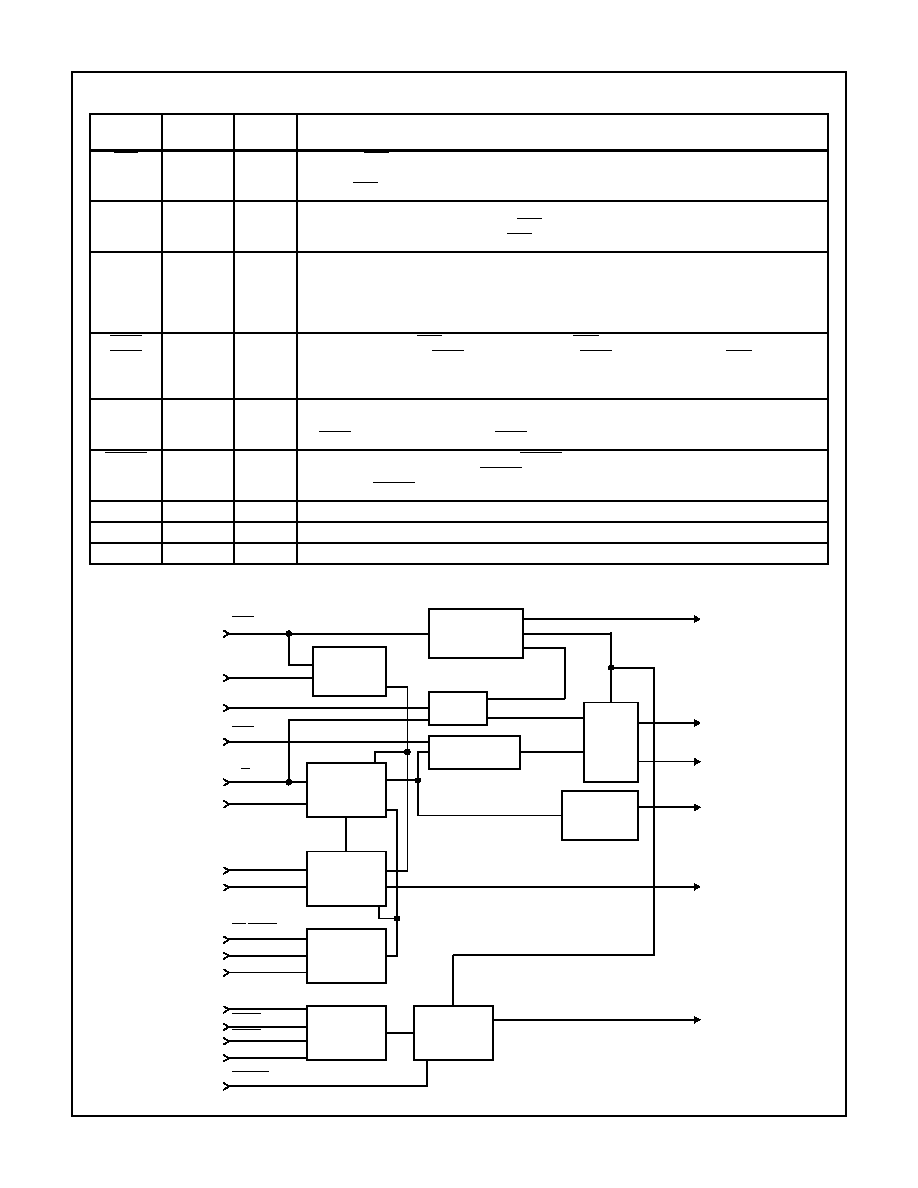
STOP LOGIC
SYNC
LOGIC
PERIPHERAL
CLOCK
(DIVIDE BY 6)
READY
SYNC
OSCILLATOR
READY
SELECT
SPEED SELECT
DIV 256 OR DIV 1
RESTART
LOGIC
CLOCK
(DIVIDE
LOGIC
BY 3)
RESET PULSE
CONDITIONING
LOGIC
RESET
CLK
CLK50
PCLK
OSC
READY
(16)
(8)
(10)
(2)
(18)
(5)
(17)
(1)
(12)
(19)
(23)
(21)
(11)
(20)
(22)
(15)
(14)
(13)
(4)
(3)
(7)
(6)
RES
START
CSYNC
SLO/FST
F/C
EFI
X2
X1
S2/STOP
S1
S0
RDY1
AEN1
AEN2
RDY2
ASYNC
RESTART
SYNC
MASTER
SELECTED
OSC
HALT
V
CC
(24)
GND (9)
OS
C
OSC
EXTERNAL
FREQ.
SELECT
82C85

300
Functional Description
The 82C85 Static Clock Controller/Generator provides sim-
ple and complete control static CMOS system operating
modes. The 82C85 supports full speed, slow, stop-clock and
stop-oscillator operation. While it is directly compatible with
the Intersil 80C86 and 80C88 CMOS 16-bit static micropro-
cessors, the 82C85 can also be used for general purpose
system clock control.
The 82C85 pinout is a superset of the 82C84A Clock Gener-
ator/Driver. 82C85 pins 1-9, 16-24 are compatible with
82C84A pins 1-9, 10-18 respectively. An 82C84A can be
placed in the upper 18 pins of an 82C85 socket and it will
operate correctly (without the ability to control the clock and
oscillator operation.) This allows dual design for simple sys-
tem upgrades. The 82C85 will also emulate an 82C84A
when pins 11-15 on the 82C85 are tied to V
CC
.
For static systems designs, separate signals are provided on
the 82C85 for stop and start control of the crystal oscillator
and clock outputs. A single control line determines 82C85
fast (crystal/EFI frequency divided by 3) or slow (crystal/EFI
frequency divided by 768) mode operation. The 82C85 also
contains a crystal controlled oscillator, clock generation
logic, complete "Ready" synchronization and reset logic.
Automatic 80C86/88 software HALT instruction decode logic
is present to ease the design of software-based clock control
systems and provide complete software control of STOP
mode operation. Restart logic insures valid clock start-up
and complete synchronization of CLK, CLK50 and PCLK.
Static Operating Modes
In static CMOS system design, there are four basic operat-
ing modes. The 82C85 Static Clock Controller supports each
of them. These modes are: FAST, SLOW, STOP-CLOCK
and STOP-OSCILLATOR. Each has distinct power and per-
formance characteristics which can be matched to the needs
of a particular system at a specific time (See Table 1).
Keep in mind that a single system may require all of these
operating modes at one time or another during normal opera-
tion. A design need not be limited to a single operating mode
or a specific combination of modes. The appropriate operating
mode can be matched to the power-performance level
needed at a specific time or in a particular circumstance.
Reset Logic
The 82C85 reset logic provides a Schmitt trigger input (RES)
and a synchronizing flip-flop to generate the reset timing.
The reset signal is synchronized to the falling edge of CLK.
A simple RC network can be used to provide power-on reset
by utilizing this function of the 82C85.
When in the crystal oscillator (F/C = LOW) or the EFI (F/C =
HIGH) mode, a LOW state on the RES input will set the
RESET output to the HIGH state. It will also restart the oscil-
lator circuit if it is in the idle state. The RESET output is guar-
anteed to stay in the HIGH state for a minimum of 16 CLK
cycles after a low-to-high transition of the RES input.
An oscillator restart count sequence will not be disturbed by
RESET if this count is already in progress. After the restart
counter expires, the RESET output will stay HIGH at least for
16 periods of CLK before going LOW. RESET can be kept high
beyond this time by a continuing low input on the RES input.
If F/C is low (crystal oscillator mode), a low state on RES
starts the crystal oscillator circuit. The stopped outputs
remain inactive, until the oscillator signal amplitude reaches
the X1 Schmitt trigger input threshold voltage and 8192
cycles of the crystal oscillator output are counted by an inter-
nal counter. After this count is complete, the stopped outputs
(CLK, CLK50, PCLK, and OSC) start cleanly with the proper
phase relationships.
This 8192 count requirement insures that the CLK, CLK50
and PCLK outputs will meet minimum clock requirements
and will not be affected by unstable oscillator characteristics
which may exist during the oscillator start-up sequence. This
sequence is also followed when a START command is
issued while the 82C85 oscillator is stopped.
Oscillator/Clock Start Control
Once the oscillator is stopped (or committed to stop) or at power-
on, the restart sequence is initiated by a HIGH state on START
or LOW state on RES. If F/C is HIGH, then restart occurs imme-
diately after the START or RES input is synchronized internally.
This insures that stopped outputs (CLK, PCLK, OSC and
CLK50) start cleanly with the proper phase relationship.
If F/C is low (crystal oscillator mode), a HIGH state on the
START input or a low state on RES causes the crystal oscil-
lator to be restarted. The stopped outputs remain stopped,
TABLE 1. STATIC SYSTEM OPERATING MODE CHARACTERISTICS
OPERATING
MODE
DESCRIPTION
POWER LEVEL
PERFORMANCE
Stop-Oscillator
All system clocks and main clock oscillator are
stopped
Maximum Savings
Slowest response due to oscillator
restart time
Stop-Clock
System CPU and peripherals clocks stop but main
clock oscillator continues to run at rated frequency
Reduced System
Power
Fast restart-no oscillator restart time
Slow
System CPU clocks are slowed while peripheral clock
and main clock oscillator run at rated frequency
Power Dissipation
Slightly Higher Than
Stop-Clock
Continuous operation at low frequency
Fast
All clocks and oscillators run at rated frequency
Highest Power
Fastest response
82C85

301
until the oscillator signal amplitude reaches the X1 Schmitt
trigger input threshold voltage and 8192 cycles of the crystal
oscillator output are counted by an internal counter. After
this count is complete, the stopped outputs (CLK, CLK50,
PCLK, and OSC) start cleanly with the proper phase rela-
tionships.
Typically, any input signal which meets the START input tim-
ing requirements can be used to start the 82C85. In many
cases, this would be the INT output from an 82C59A CMOS
Priority Interrupt Controller (See Figure 1). This output,
which is active high, can be connected to both the 82C85
START pin and to the appropriate interrupt request input on
the microprocessor.
When the INT output becomes active, the oscillator/clock cir-
cuit on the 82C85 will restart. Upon completion of the appro-
priate restart sequence, the CLK signal to the CPU will
become active. The CPU can then respond to the still pend-
ing interrupt request.
If the 82C59A/82C85 restart combination is used in conjunc-
tion with an 82C55A STOP control, the 82C55A must be ini-
tialized prior to the 82C59A after reset. The 82C59A
interrupt output is driven high at reset, causing the 82C85 to
remain in the START mode regardless of the state of the
S2/STOP input. This will avoid stopping the 82C85 due to
negative transitions on the S2/STOP input which may occur
during a mode change on the 82C55A or during the opera-
tion of any peripheral I/O device prior to initialization.
Another method of insuring proper operation of the START
function upon reset or system initialization is to bias the
S2/STOP input low with an external pull-down resistor. The
S2/STOP input will remain low until driven high by the
82C55A port pin or by external logic. This insures that the
82C85 STOP command (HHH prior to LHH requirement on
the status inputs) will not be satisfied. To minimize power
dissipation in this case (using a pulldown resistor), the
S2/STOP input should be normally LOW and pulsed HIGH
to develop the necessary HHH-to-LHH STOP sequence. In
this manner, the output driving the S2/STOP input will be
normally LOW and will not be driving to the opposite state of
the pull-down resistor.
Fast Mode
The most common operating mode for a system is the FAST
mode. In this mode, the 82C85 operates at the maximum fre-
quency determined by the main oscillator or EFI frequency.
82C59A
82C85
START
CLK
S0
S1
S2/STOP
SLO/FST
80C86/88
INTR
CLK
PA0 PA1
82C55A
INT
V
CC
FIGURE 1. CMOS PERIPHERAL CONTROL OF 82C85 STOP,
START AND SLOW/FAST OPERATIONS
TABLE 2. TYPICAL SYSTEM POWER SUPPLY CURRENT FOR STATIC CMOS OPERATING MODES
FAST
SLOW
STOP-CLOCK STOP-OSC
CPU Frequency
5MHz
20 KHz
DC
DC
XTAL Frequency
15MHz
15MHz
15MHz
DC
ICC
82C85
24.7mA
16.9mA
14.1mA
24.4mA
80C88
23.8mA
173.0mA
106.6mA
106.6mA
82C82
1.7mA
6.5mA
1.0mA
1.0mA
82C86
1.4mA
14.0mA
1.0mA
1.0mA
82C88
3.5mA
14.3mA
3.8mA
3.8mA
82C52
151.2mA
72.0mA
1.0mA
1.0mA
82C54
943.0mA
915.0mA
3.5mA
1.0mA
82C55A
3.2mA
1.2mA
1.0mA
1.0mA
82C59A
580.0mA
520.0mA
1.0mA
1.0mA
74HCXX + other
2.9mA
10.0mA
90.0mA
90.0mA
HM-6516
820.0mA
32.0mA
1.9mA
1.9mA
HM-6616
6.3mA
52.5mA
12.0mA
12.0mA
Total
66.8mA
18.9mA
14.3mA
244.7mA
All measurements taken at room temperature, V
CC
= +5.0V. Power supply current levels will be dependent upon system configuration and
frequency of operation.
82C85

302
FAST mode operation is enabled by each of two conditions:
∑ The SLO/FST input is HIGH and a START or reset
command is issued
∑ The SLO/FST input is held HIGH for at least 6 oscillator or
EFI cycles.
Alternate Operating Modes
Using alternate modes of operation (slow, stop-clock, stop-
oscillator) will reduce the average system operating power
dissipation in a static CMOS system (See Table 2). This
does not mean that system speed or throughput must be
reduced. When used appropriately, the slow, stopclock,
stop-oscillator modes can make your design more power
efficient while maintaining maximum system performance.
Stop-Oscillator Mode
When the 82C85 is stopped while in the crystal mode (F/C
LOW), the oscillator, in addition to all system clock signals
(CLK, CLK50 and PCLK), are stopped. CLK and CLK50 stop
in the high state. PCLK stops in it's current state (high or low).
With the oscillator stopped, 82C85 power drops to it's lowest
level. All clocks and oscillators are stopped. All devices in
the system which are driven by the 82C85 go into the lowest
power standby mode. The 82C85 also goes into standby
and requires a power supply current of less than 100
µ
A.
Stop-Clock Mode
When the 82C85 is in the EFI mode (F/C HIGH) and a STOP
command is issued, all system clock signals (CLK, CLK50,
and PCLK) are stopped. CLK and CLK50 stop in the high
state when F/C is low and may stop in either the high or low
state when F/C is high. PCLK stops in its current state (high
or low).
The 82C85 can also provide it's own EFI source simply by
connecting the OSC output to the EFI input and pulling the
F/C input HIGH. This puts the 82C85 into the External Fre-
quency Mode using it's own oscillator as an external source
signal (See Figure 2). In this configuration, when the 82C85
is stopped in the EFI mode, the oscillator continues to run.
Only the clocks to the CPU and peripherals (CLK, CLK50
and PCLK) are stopped.
Oscillator/Clock Stop Operation
Three control lines determine when the 82C85 clock outputs
or oscillator will stop. These are S0, S1 and S2/STOP.
These three lines are designed to connect directly to the
MAXimum mode 80C86 and 80C88 status lines or to be
driven by external I/O signals (such as an 82C55A output
port).
In the MAXimum mode configuration, the 82C85 will auto-
matically recognize a software HALT command from the
80C86 or 80C88 and stop the system clocks or oscillator.
This allows complete software control of the STOP function.
If the 80C86 or 80C88 is used in the MINimum mode, the
82C85 can be controlled using the S2/STOP input (with S0
and S1 held high). This can be done using an external I/O
control line, such as from an 82C55A or by decoding the
state of the 80C86 MINimum mode status signals.
82C85 status inputs S2/STOP, S1, S0 are sampled on the
rising edge of CLK. The oscillator (F/C LOW only) and clock
outputs are stopped by S2/STOP, S1, S0 being in the LHH
state on a low-to-high transition of CLK. This LHH state must
follow a passive HHH state occurring on the previous low-to-
high CLK transition. CLK and CLK50 will stop in the logic
HIGH state after two additional complete cycles of CLK.
PCLK stops in it's current state (HIGH or LOW). This is true
for both SLOW and FAST mode operation.
80C86/88 Maximum Mode Clock Control
The 82C85 STOP function has been optimized for 80C86/88
MAXimum mode operation. In this mode, the three 82C85 sta-
tus inputs (S2/STOP, S1, S0) are connected directly to the
MAXimum mode status lines (S2, S1, S0) of the Intersil
80C86 or 80C88 static CMOS microprocessors (See Figure
3).
When in the MAXimum mode, the 80C86/88 status lines
identify which type of bus cycle the CPU is starting to exe-
cute. 82C85 S2/STOP, S1 and S0 control input logic will rec-
ognize a valid MAXimum mode software HALT executed by
the 80C86 or 80C88. Once this state has been recognized,
the 82C85 stops the clock (F/C HIGH) and oscillator (F/C
LOW) operation.
FIGURE 2. STOP-CLOCK MODE USING 82C85 IN EFI MODE
WITH OSCILLATOR AS FREQUENCY SOURCE
X1
X2
EFI
F/C
S2/STOP
S1
S0
START
OSC
V
CC
STOP
CONTROL
START
CONTROL
MN/MX
S0
S1
S2
S0
S1
S2/STOP
82C85
80C86/88
FIGURE 3. 82C85 STOP CONTROL USING 80C86/88
MAXIMUM MODE STATUS LINES
82C85
303
The 82C85 S2/STOP, S1 and S0 control lines were
designed to detect a passive 111 state followed by a HALT
011 logic state before recognizing the HALT instruction and
stopping the system clocks. In the MAXimum mode, the
80C86/88 status lines go into a passive (no bus cycle) logic
111 state prior to executing a HALT instruction. The qualifi-
cation of a passive no bus cycle logic 111 state insures that
random transitions of the status lines into a logic 011 state
will not stop the system clock. This is necessary since the
status lines of the 80C86/88 transition through an unknown
state during T3 of the bus cycle.
Once the HALT instruction is decoded by the 82C85, either
the oscillator is stopped (STOP-OSCILLATOR mode F/C
tied low) or the external frequency source is gated off inter-
nally (STOP-CLOCK mode F/C HIGH). When the HALT
instruction is decoded with F/C low, the CLK and CLK50 will
be stopped in a logic high state after 2 additional cycles of
the clock. PCLK stops in it's current state (high or low). This
is true for both SLOW and FAST mode operation. The HALT
instruction is detected in the same manner whether the
82C85 is in the SLOW or FAST mode.
Independent Stop Control for Minimum Mode Operation
When the 80C86 and 80C88 microprocessors are config-
ured in MINimum Mode (MN/MX pin tied high), their status
lines S0, S1, and S2 assume alternate functions. The logic
states and sequences (passive before a HALT) necessary
for automatic HALT detect in the 82C85 do not occur as in
the MAXimum mode. The 82C85 controller cannot use the
microprocessor status lines to detect a software Halt instruc-
tion when operating in MINimum mode.
However, the negative edge-activated S2/STOP pin pro-
vides a simple means for clock control in MINimum mode
80C86 and 80C88 systems. S2/STOP can be used as an
independent STOP control when S1 and S0 are held in the
logical HIGH state. Keeping the S0 and S1 inputs at a logic 1
level and transitioning S2/STOP from high to low will meet
the passive 111 state prior to a 011 state requirement of the
82C85. This feature allows 82C85 operation with the 80C86
and 80C88 in the MINimum mode, provides compatibility
with other static CMOS microprocessors and allows maxi-
mum flexibility in a system.
With S2/STOP being used as a stand-alone STOP com-
mand line, system clocks can be controlled via an 82C55A
programmable peripheral interface or other similar interface
circuits. This is accomplished by driving the S2/STOP input
with a PORT pin on the 82C55A (See Figure 1). The
82C55A port pin should be configured as an output and must
present a logic HIGH to the S2/STOP input for at least one
CLK cycle, followed by a LOW state. This will meet the
82C85 status input requirement of 111 followed by a 011.
When a logic 0 is written to a 82C55A port pin, the S2/ STOP
pin is pulled low, stopping the system clocks (CLK, CLK50,
PCLK). In essence, the 82C85 is software controlled via the
82C55A. As with the SLO/FST interface, PORT C is a logical
choice for this job since the individual bit set and reset com-
mands available for this port make control of the S2/STOP
input simple.
A START command issued to the 82C85 will override a
STOP command and the 82C85 will begin normal operation.
The low state of the negative-edge triggered S2/STOP input
will not prohibit the clocks from restarting. After a START or
RES command, the 82C85 must see a passive (111) state
followed by a HALT (011) state to stop the system clocks. To
accomplish this, the 82C55A port output must be brought
high and then returned low again for the 82C85 to recognize
the next STOP command.
External Decode Adds Halt Control
SS0, IO/M and DT/R can identify a MINimum mode 80C88
HALT execution. During T2 of the system timing (while ALE
is high), SS0, IO/M, and DT/R go into a 111 state when the
80C88 is executing a software HALT. These signals cannot
be tied directly to the S2/STOP, S1 and S0 inputs since they
are not guaranteed to go into a passive state prior to their
111 state. These signals can be decoded during the time
ALE is high to indicate a software HALT execution.
Slow Mode
When continuous operation is critical but power consump-
tion remains a concern, the 82C85 SLOW mode operation
provides a lower frequency at the CLK and CLK50 outputs
(crystal/EFI frequency divided by 768). The frequency of
PCLK is unaffected. The SLOW mode allows the CPU and
the system to operate at a reduced rate which, in turn,
reduces system power.
For example, the operating power for the 80C86 or 80C88
CPU is 10mA/MHz of clock frequency. When the SLOW
mode is used in a typical 5MHz system, CLK and CLK50 run
at approximately 20kHz. At this reduced frequency, the aver-
age operating current of the CPU drops to 200
µ
A. Adding
the 80C86/88 500
µ
A standby current brings the total current
to 700
µ
A.
While the CPU and peripherals run slower and the 82C85
CLK and CLK50 outputs switch at a reduced frequency, the
main 82C85 oscillator is still running at the maximum fre-
quency (determined by the crystal or EFI input frequency.)
Since CMOS power is directly related to operating fre-
quency, 82C85 power supply current will typically be
reduced by 15-20%.
Clock Slow/Fast Operation
The SLO/FST input determines whether the CLK and CLK50
outputs run at full speed (crystal or EFI frequency divided by
3) or at slow speed (crystal or EFI frequency divided by 768)
(See Figure 4). When in the SLOW mode, 82C85 stop-clock
and stop-oscillator functions operate in the same manner as
in the FAST mode.
Internal logic requires that the SLO/FST pin be held low for
at least 195 oscillator or EFI clock pulses before the SLOW
mode command is recognized. This requirement eliminates
unwanted FAST-to-SLOW mode frequency changes which
could be caused by glitches or noise spikes.
To guarantee FAST mode recognition, the SLO/FST pin
must be held high for at least 6 OSC or EFI pulses. The
82C85 will begin FAST mode operation on the next PCLK
82C85
304
edge after FAST command recognition. Proper CLK and
CLK 50 phase relationships are maintained and minimum
pulse width specifications are met.
FAST-to-SLOW or SLOW-to-FAST mode changes will occur
on the next rising or falling edge of PCLK. It is important to
remember that the transition time for operating frequency
changes, which are dependent upon PCLK, will vary with the
82C85 oscillator or EFI frequency.
Slow Mode Control
The 82C55A programmable peripheral interface can be
used to provide control of the SLO/FST pin by connecting a
port pin of the 82C55A directly to the SLO/FST pin (See Fig-
ure 1). With the port pin configured as an output, software
control of the SLO/FST pin is provided by simply writing a
logical one (FAST mode) or logical zero (SLOW Mode) to
the corresponding port. PORT C is well-suited for this func-
tion due to it's bit set and reset capabilities. Since PCLK con-
tinues to run at a frequency equal to the oscillator or EFI
frequency divided by 6, it can be used by other devices in
the system which need a fixed high frequency clock. For
example, PCLK could be used to clock an 82C54 program-
mable interval timer to produce a real-time clock for the sys-
tem or as a baud rate generator to maintain serial data
communications during SLOW mode operation.
Oscillator
The oscillator circuit of the 82C85 is designed primarily for
use with an external parallel resonant, fundamental mode
crystal from which the basic operating frequency is derived.
The crystal frequency should be selected at three times the
required CPU clock. X1 and X2 are the two crystal input con-
nections. The output of the oscillator is buffered and avail-
able at the OSC output (pin 18) for generation of other
system timing signals.
For the most stable operation of the oscillator (OSC) output
circuit, two capacitors (C1 = C2) are recommended. Capaci-
tors C1 and C2 are chosen such that their combined capaci-
tance matches the load capacitance as specified by the
crystal manufacturer. This insures operation within the fre-
quency tolerance specified by the crystal manufacturer.
The crystal/capacitor configuration and the formula used to
determine the capacitor values are shown in Figure 4. Crys-
tal Specifications are shown in Table 3.
Frequency Source Selection
The F/C input is a strapping pin that selects either the crystal
oscillator or the EFI input as the source frequency for clock
generation. If the EFI input is selected as the source, the
oscillator section (OSC output) can be used independently
for another clock source. If a crystal is not used, then crystal
input X1 (pin 23) must be tied to V
CC
or GND and X2 (pin
22) should be left open. If the EFI mode is not used, then EFI
(pin 20) should be tied to V
CC
or GND.
TABLE 3. CRYSTAL SPECIFICATIONS
PARAMETER
TYPICAL CRYSTAL
SPECIFICATION
Frequency
2.4 to 25MHz
Type of Operation
Parallel Resonant, Fund. Mode
Load Capacitance
20 or 32pF
RSERIES (Max)
35X (f = 25MHz, C
L
= 32pF)
66X (f = 25MHz, C
L
= 20pF)
CT
C1 C2
∑
C1 C2
+
----------------------
(Including Stray Capacitance)
=
(EQ. 1)
C
1
C
2
X2
X1
CRYSTAL
2.4 - 25MHz
FIGURE 4. 82C85 CRYSTAL CONNECTION
FIGURE 5. SLO/FST TIMING OVERVIEW
EFI
OR
OSC
PCLK
SLO/FST
CLK
CLK50
82C85

305
Clock Generator
The clock generator consists of two synchronous divide-by-
three counters with special clear inputs that inhibit the count-
ing. One counter generates a 33% duty cycle waveform
(CLK) and the other generates a 50% duty cycle waveform
(CLK50). These two counters are negative-edge synchro-
nized, with the low-going transitions of both waveforms
occurring on the same oscillator transition. The CLK and
CLK50 output frequencies are one-third of the base input
frequency when SLO/FST is high and are equal to the base
input frequency divided by 768 when SLO/FST is low.
The CLK output is a 33% duty cycle clock signal designed to
drive the 80C86 and 80C88 microprocessors directly.
CLK50 has a 50% duty cycle output synchronous with CLK,
designed to drive co-processors and peripherals requiring a
50% duty cycle clock. When SLO/FST is high, CLK and
CLK50 have output frequencies which are 1/3 that of EFI/
OSC. When SLO/FST is low, CLK and CLK50 have output
frequencies which are OSC (EFI) divided by 768.
PCLK is a peripheral clock signal with an output frequency
equal to the oscillator or EFI frequency divided by 6. PCLK
has a 50% duty cycle. PCLK is unaffected by SLO/FST.
When the 82C85 is placed in the STOP mode, PCLK will
remain in it's current state (logic high or logic low) until a
RESET or START command restarts the 82C85 clock cir-
cuitry. PCLK is negative-edge synchronized with CLK and
CLK50.
Clock Synchronization
The clock synchronization (CSYNC) input allows the output
clocks to be synchronized with an external event (such as
another 82C85 or 82C84A clock signal). CSYNC going
active causes all clocks (CLK, CLK50 and PCLK) to stop in
the HIGH state.
It is necessary to synchronize the CSYNC input to the EFI
clock external to the 82C85. This is accomplished with two
flip-flops when synchronizing two 82C85s and with three flip-
flops when synchronizing an 82C85 to an 82C84A (See Fig-
ure 6). Multiple external flip-flops are necessary to minimize
the occurrence of metastable (or indeterminate) states.
Ready Synchronization
Two READY inputs (RDY1, RDY2) are provided to accom-
modate two system busses. Each READY input is qualified
by (AEN1 and AEN2, respectively). The AEN signals vali-
date their respective RDY signals.
Synchronization is required for all asynchronous active-
going edges of either RDY input to guarantee that the RDY
set up and hold times are met. Inactive-going edges of RDY
in normally ready systems do not require synchronization but
must satisfy RDY setup and hold as a matter of proper sys-
tem design.
The ASYNC input defines two modes of READY synchroni-
zation operation. When ASYNC is LOW, two stages of syn-
chronization are provided for active READY input signals.
Positive-going asynchronous READY inputs will first be syn-
chronized to flip-flop one at the rising edge of CLK (requiring
a setup time TR1VCH) and then synchronized to flip-flop two
at the next falling edge of CLK, after which time the READY
output will go HIGH.
Negative-going asynchronous READY inputs will be syn-
chronized directly to flip-flop two at the falling edge of CLK,
after which time the READY output will go inactive. This
mode of operation is intended for use by asynchronous (nor-
mally not ready) devices in the system which cannot be
guaranteed by design to meet the required RDY setup timing
(TR1VCL) on each bus cycle.
When ASYNC is high or left open, the first READY flip-flop is
bypassed in the READY synchronization logic. READY
inputs are synchronized by flip-flop two on the falling edge of
CLK before they are presented to the processor. This mode
is available for synchronous devices that can be guaranteed
to meet the required RDY setup time. ASYNC can be
changed on every bus cycle to select the appropriate mode
of synchronization for each device in the system.
EFI
82C85
CSYNC
CSYNC
82C84A
CSYNC WITH 82C85(s)
CLOCK
SYNC
EFI
D
Q
>
>
>
D
Q
Q
D
(TO OTHER
82C85s)
FIGURE 6. 82C85 AND 82C84A CSYNC SYNCHRONIZATION
METHODS
82C85

306
Absolute Maximum Ratings
Thermal Information
Supply Voltage . . . . . . . . . . . . . . . . . . . . . . . . . . . . . . . . . . . . . +8.0V
Input, Output or I/O Voltage . . . . . . . . . . . GND -0.5V to V
CC
+0.5V
ESD Classification . . . . . . . . . . . . . . . . . . . . . . . . . . . . . . . . Class 1
Operating Conditions
Operating Voltage Range . . . . . . . . . . . . . . . . . . . . . +4.5V to +5.5V
Operating Temperature Range
C82C85. . . . . . . . . . . . . . . . . . . . . . . . . . . . . . . . . . .0
o
C to +70
o
C
I82C85 . . . . . . . . . . . . . . . . . . . . . . . . . . . . . . . . . -40
o
C to +85
o
C
M82C85 . . . . . . . . . . . . . . . . . . . . . . . . . . . . . . . -55
o
C to +125
o
C
Thermal Resistance (Typical)
JA
(
o
C/W)
JC
(
o
C/W)
CERDIP Package . . . . . . . . . . . . . . . . .
70
16
CCC Package . . . . . . . . . . . . . . . . . . . .
75
18
PLCC Package . . . . . . . . . . . . . . . . . . .
65
N/A
Storage Temperature Range . . . . . . . . . . . . . . . . .-65
o
C to +150
o
C
Maximum Junction Temperature Ceramic Package . . . . . . . +175
o
C
Maximum Junction Temperature Plastic Package . . . . . . . . +150
o
C
(Soldering 10s)
Maximum Lead Temperature (Soldering 10s). . . . . . . . . . . . +300
o
C
(PLCC - Lead Tips Only)
Die Characteristics
Gate Count . . . . . . . . . . . . . . . . . . . . . . . . . . . . . . . . . . . . 500 Gates
CAUTION: Stresses above those listed in "Absolute Maximum Ratings" may cause permanent damage to the device. This is a stress only rating and operation
of the device at these or any other conditions above those indicated in the operational sections of this specification is not implied.
DC Electrical Specifications
V
CC
= 5.0V 10%; T
A
= 0
o
C to +70
o
C (C82C85);
T
A
= -40
o
C to +85
o
C (I82C85);
T
A
= -55
o
C to +125
o
C (M82C85)
SYMBOL
PARAMETER
MIN
MAX
UNITS
TEST CONDITIONS
V
IH
Logical One Input Voltage
2.0
2.2
-
V
V
C82C85, I82C85
M82C85
V
IHR
Reset Input High Voltage
2.8
-
V
V
IL
Logical Zero Input Voltage
-
0.8
V
Note 1
V
T+
- V
T
Reset Input Hysteresis
0.25
-
V
V
OH
Logical One Output Voltage
V
CC
-0.4
-
V
I
OH
= -5.0 mA (CLK, CLK50)
I
OH
= -1.0mA (X2)
I
OH
= -2.5mA (all other outputs)
V
OL
Logical Zero Output Voltage
-
0.4
V
I
OL
= +2.5mA (X2)
I
OL
= +5.0mA (all other outputs)
II
Input Leakage Current
-1.0
1.0
µ
A
V
IN
= V
CC
or GND, except DIP
Pins 11 - 15, 21, 23
IBHH
Bus-hold High Leakage Current
-10
-200
µ
A
V
IN
= 3.0V; Pins 11 - 15, 21
ICCSB
Standby Power Supply Current
-
100
µ
A
82C85 in HALT state with oscillator
stopped
ICCOP
Operating Power Supply Current
-
50
mA
Crystal Frequency = 15MHz, outputs
open, inputs = GND or V
CC
-
70
mA
Crystal Frequency = 25MHz, outputs
open, inputs = GND or V
CC
ICCSLOW
Slow Mode Operating Current
-
40
mA Crystal
Freq = 15MHz
Outputs Open; SLO/FST = GND,
START = V
CC
, Other inputs - V
IN
=
V
CC
or GND
-
60
mA Crystal
Freq = 25MHz
NOTE:
1. For CSYNC, V
IL
= GND
Capacitance
T
A
= 25
o
C
SYMBOL
PARAMETER
TYPICAL
UNITS
TEST CONDITIONS
C
IN
Input Capacitance
15
pF
FREQ = 1MHz, all measurements are referenced to device
GND
C
OUT
Output Capacitance
20
pF
82C85
307
AC Electrical Specifications
V
CC
= 5V
±
10%;T
A
= 0
o
C to +70
o
C (C82C85);
T
A
= -40
o
C to +85
o
C (I82C85);
T
A
= -55
o
C to +125
o
C (M82C85)
SYMBOL
PARAMETER
LIMITS
UNITS
CONDITIONS
MIN
MAX
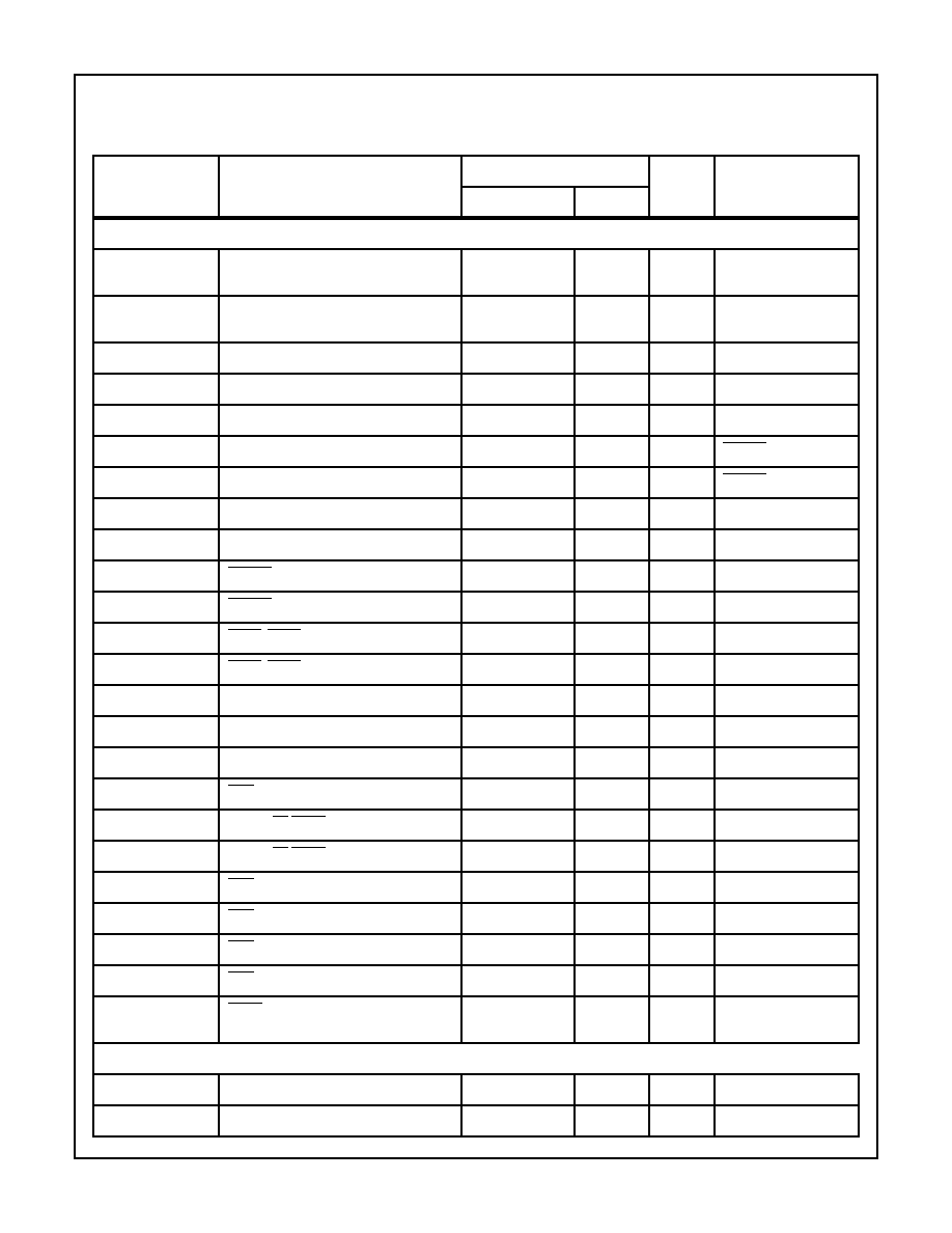
TIMING REQUIREMENTS
(1)
TEHEL
External Frequency HIGH Time
15
-
ns
90%-90% V
IN
, Note 1,
f = 25MHz
(2)
TELEH
External Frequency LOW Time
15
-
ns
10%-10% V
IN
, Note 1,
f = 25MHz
(3)
TELEL
EFI or Crystal Period
40
-
ns
Note 1
(4)
TEFIDC
External Frequency Input Duty Cycle
45
55
%
f = 25MHz, Note 1
(5)
Fx
Crystal Frequency
2.4
25
MHz
Note 1
(6)
TR1VCL
RDY1, RDY2 Active Setup to CLK
35
-
ns
ASYNC = HIGH
(7)
TR1VCH
RDY1, RDY2 Active Setup to CLK
35
-
ns
ASYNC = LOW
(8)
TR1VCL
RDY1, RDY2 Inactive Setup to CLK
35
-
ns
(9)
TCLR1X
RDY1, RDY2 Hold to CLK
0
-
ns
(10)
TAYVCL
ASYNC Setup to CLK
50
-
ns
(11)
TCLAYX
ASYNC Hold to CLK
0
-
ns
(12)
TA1VR1V
AEN1, AEN2 Setup to RDY1, RDY2
15
-
ns
(13)
TCLA1X
AEN1, AEN2 Hold to CLK
0
-
ns
(14)
TYHEH
CSYNC Setup to EFI
10
-
ns
(15)
TEHYL
CSYNC Hold to EFI
10
-
ns
(16)
TYHYL
CSYNC Pulse Width
2TELEL
-
ns
(17)
TI1HCL
RES Setup to CLK
65
-
ns
Note 2
(18)
TSVCH
S0, S1, S2/STOP Setup to CLK
35
-
ns
(19)
TCHSV
S0, S1, S2/STOP Hold to CLK
35
-
ns
(20)
TRSVCH
RES, START Setup to CLK
65
-
ns
Note 2
(21)
TSHSL
RES (Low) or START (High) Pulse Width
TCLCLs3
-
ns
(22)
TSFPC
SLO/FST Setup to PCLK
TEHEL + 100
-
ns
Note 2
(23)
TSTART
RES or START Valid to CLK Low
2TELEL + 2
-
ns
(24)
TSTOP
STOP Command Valid to CLK High
2TCHCH +
TRSVCH
3TCHCH
+ 34
ns
TCHCH = TCLCL
TIMING RESPONSES
(25)
TCLCL
CLK/CLK50 Cycle Period
125
-
ns
Note 1
(26)
TCHCL
CLK HIGH Time
(1/3 TCLCL)+2
-
ns
82C85

308
(27)
TCLCH
CLK LOW Time
(2/3 TCLCL)-15
-
ns
(28)
T5CHCL
CLK50 HIGH Time
(1/2 TCLCL)-7.5
-
ns
(29)
T5CLCH
CLK50 LOW Time
(1/2 TCLCL)-7.5
-
ns
(30)
TCH1CH2
CLK/CLK50 Rise Time
-
8
ns
1.0V to 3.5V
(31)
TCL2CL1
CLK/CLK50 Fall Time
-
8
ns
1.0V to 3.5V
(32)
TPHPL
PCLK HIGH Time
TCLCL-20
-
ns
(33)
TPLPH
PCLK LOW Time
TCLCL-20
-
ns
(34)
TRYLCL
Ready Inactive to CLK
-8
-
ns
Note 4
(35)
TRYHCH
Ready Active to CLK
2/3(TCLCL)-15
-
ns
Note 3
(36)
TCLIL
CLK to Reset Delay
-
40
ns
(37)
TCLPH
CLK to PCLK HIGH Delay
-
22
ns
(38)
TCLPL
CLK to PCLK LOW Delay
-
22
ns
(39)
TOST
Start/Reset Valid to Clock LOW
-
2
ms
Typ. - Note 8
(40)
TOLOH
Output Rise Time (except CLK)
-
15
ns
From 0.8V to 2.0V
(41)
TOHOL
Output Fall Time (except CLK)
-
12
ns
From 2.0V to 0.8V
(42)
TRST
RESET output HIGH Time
16 x TCLCL
-
ns
(43)
TCLC50L
CLK LOW to CLK50 LOW Skew
-
5
ns
NOTES:
1. Slow and Fast Modes.
2. Setup and hold necessary only to guarantee recognition at next clock.
3. Applies only to T3, TW states.
4. Applies only to T2 states.
5. All timing delays are measured at 1.5V unless otherwise noted.
6. Input signals must switch between V
IL
max - 0.4 and V
IH
min + 0.4 volts
7. Timing measurements made with EFI duty cycle = 50%.
8. Oscillator start up time depends on several factors including crystal frequency, crystal manufacturer, capacitive load, temperature, power
supply voltage, etc. This parameter is given for information only.
9. Output signals switch between V
OH
and V
OL
unless otherwise specified.
AC Electrical Specifications
V
CC
= 5V
±
10%;T
A
= 0
o
C to +70
o
C (C82C85);
T
A
= -40
o
C to +85
o
C (I82C85);
T
A
= -55
o
C to +125
o
C (M82C85)
(Continued)
SYMBOL
PARAMETER
LIMITS
UNITS
CONDITIONS
MIN
MAX
82C85

309
Timing Waveforms
FIGURE 7. WAVEFORMS FOR CLOCKS
NOTE: All Timing Measurements are made at 1.5V, Unless Otherwise Noted.
FIGURE 8. WAVEFORMS FOR READY SIGNALS (FOR ASYNCHRONOUS DEVICES)
CLK AND CLK50
1.0V
3.5V
(30) TCH1CH2
TCL2CL1 (31)
TPLPH
(33)
TPHPL
(32)
(37)
TCLPH
(28)
T5CHCL
TCLPL
(38)
T5CLCH (29)
(26)
TCHCL
TCLCH
(27)
TCLC50L
(43)
TELEH
(2)
(3)
TELEL
(1)
TEHEL
EFI I
OSC 0
CLK 0
CLK50 0
PCLK 0
CSYNC I
(15)
TEHYL
(16)
TYHYL
(14)
TYLEH
TCLCL (25)
CLK
RDY1.2
AEN1.2
ASYNC
READY
(12) TA1VR1V
(7) TRIVCH
(11) TCLAYX
(34) TRYLCL
(13) TCLA1X
(8) TRILCL
(9)
TCLR1X
(35)
TRYHCH
(10)
TAYVCL
(9)
TCLR1X
82C85

310
FIGURE 9. WAVEFORMS FOR READY SIGNALS (FOR SYNCHRONOUS DEVICES)
FIGURE 10. CLOCK STOP (F/C HIGH OR F/C LOW)
NOTE: When F/C is low, CLK and CLK50 stop high. When F/C is high, CLK and CLK50 may stop either high or low.
Timing Waveforms
(Continued)
(6)
TRIVCL
(9)
TCLRIX
(10)
TAYVCL
(35)
TRYHCH
(34)
TRYLCL
(8)
TRILCL
(9)
TCLR1X
TCLA1X
(12) TA1VRIV
TCLAYX
(13)
(11)
CLK
RDY1, 2
AEN1, 2
ASYNC
READY
TSTOP
(24)
(18)
TSVCH
(18)
TSVCH
TCHSX (19)
TRSVCH (20)
TCHSX (19)
(SEE NOTE)
EFI
CLK
CLK50
PCLK
S0
S1
S2/STOP
RES
START
82C85
311
FIGURE 11. CLOCKS START (F/C HIGH)
FIGURE 12. CLOCK START (F/C LOW)
NOTE: Start up count begins when the crystal oscillator reaches a suitable threshold level.
Timing Waveforms
(Continued)
EFI
CLK
CLK50
PCLK
S0
S1
S2/STOP
RES
START
(23) TSTART
(39)
TOST
8192 CYCLES
CRYSTAL
OSCILLATOR
STARTUP TIME
(21)
TSHSL
START
X1
CLK50
PCLK
CLK
82C85

312
FIGURE 13. RESET TIMING (CLK RUNNING WITH F/C LOW-OSC MODE)
(CLK RUNNING-OR STOPPED WITH F/C HIGH EFI MODE)
FIGURE 14. RESET TIMING (OSCILLATOR STOPPED, F/C LOW)
NOTE: CLK, CLK50, PCLK Remain in the High State until RES goes high and 8192 valid oscillator cycles have been registered by the 82C85
internal counter (TOST time period). After RES goes high and CLK, CLK50, PCLK become active, the RESET output will remain high
for minimum of 16 CLK cycles (TRST).
Timing Waveforms
(Continued)
RES
CLK
RESET
(21) TSHSL
(17)
TI1HCL
(36)
TCLIL
(42)
TRST
(36)
TCLIL
(17)
TI1HCL
RES
(21) TSHSL
CLK
RESET
OSCILLATOR
STARTUP
TIME
X1
(39)
TOST
8192
CYCLES
(42)
TRST
(36)
TCLIL
82C85

313
FIGURE 15. SLO/FST TIMING OVERVIEW
NOTE: See Fast to Slow Clock Mode Transition for Detailed Timing; See Slow to Fast Clock Mode Transition for Detailed Timing
FIGURE 16. FAST TO SLOW CLOCK MODE TRANSITION
NOTE: IF TSFPC is not met on one edge of PLCK. SLO/FST will be recognized on the next edge of PLCK.
Timing Waveforms
(Continued)
EFI
OR
OSC
PCLK
SLO/FST
CLK
CLK50
EFI
OR
OSC
PCLK
TSFPC
(22)
(SEE NOTE)
SLO/FST
CLK
CLK50
TSFPC
(22)
(SEE NOTE)
197 TO 200 EFI
OR OSC CYCLES
82C85

314
FIGURE 17. SLOW TO FAST CLOCK MODE TRANSITION
NOTE: IF TSFPC is not met on one edge of PLCK. SLO/FST will be recognized on the next edge of PLCK.
Timing Waveforms
(Continued)
EFI
OR
OSC
PCLK
TSFPC
(22)
(SEE NOTE)
SLO/FST
CLK
CLK50
TSFPC
(22)
(SEE NOTE)
6 EFI
PULSES
82C85
315
A.C. Testing Input, Output Waveform
Test Load Circuits
PASSIVE LOAD
R = 360 at V = 2.25 for CLK and CLK50 outputs
R = 470 at V = 2.87 for all other outputs (Except X2)
NOTES:
1. C
L
= 100pF for CLK and CLK50 output
2. C
L
= 50pF minimum for all other outputs
3. C
L
= Includes probe and jig capacitance
DYNAMIC LOAD
I
OL
= 5mA, IOH = -5mA for CLK and CLK50 outputs
I
OL
= 5mA, IOH = -2.5mA for all other outputs (Except X2)
I
OL
= 2.5mA, IOH = -1.0mA for X2 output (DC Performance
characteristic only)
V
TRIP
= 1.4V
TCHCL, TCLCH LOAD CIRCUIT (USING X1, X2)
TCHCL, TCLCH LOAD CIRCUIT (USING EFI)
TRYLCL, TRYHCH LOAD CIRCUIT (USING X1, X2)
TRYLCL, TRYHCH LOAD CIRCUIT (USING EFI)
V
R
FROM OUTPUT
UNDER TEST
CL
SEE NOTE 3
V
R
FROM OUTPUT
UNDER TEST
CL
SEE NOTE 3
C1
C2
X1
X2
CSYNC
CLK
F/C
LOAD
(SEE NOTE 1)
LOAD
(SEE NOTE 1)
CLK50
EF1
CSYNC
CLK
F/C
V
CC
PULSE
GENERATOR
LOAD
(SEE NOTE 1)
LOAD
(SEE NOTE 1)
CLK50
C1
C2
X1
X2
CLK
LOAD
(SEE NOTE 1)
LOAD
(SEE NOTE 2)
CSYNC
F/C
AEN2
PULSE
GENERATOR
TRIGGER
V
CC
24MHZ
READY
OSC
AEN1
RDY2
EF1
CLK
LOAD
(SEE NOTE 1)
F/C
V
CC
PULSE
GENERATOR
CSYNC
RDY2
AEN2
LOAD
(SEE NOTE 2)
AEN1
READY
TRIGGER
PULSE
GENERATOR
INPUT
V
IH
+ 0.4V
V
IL
+ 0.4V
1.5V
1.5V
V
OH
V
OL
OUTPUT
82C85

Burn-In Circuits
MD82C85 CERDIP
MR82C85 CLCC
BOTTOM VIEW
NOTES:
1. V
CC
= 5.5V
±
0.5V, GND = 0V
2. V
IH
= 4.5V
±
10%
3. V
IL
= -0.2 to 0.4V
4. R
1
= 100k
,
±
5%
5. R
2
= 10k
,
±
5%
6. R
3
= 47k
,
±
5%
7. R
4
= 470k
,
±
5%
8. C1 = 0.01
µ
F (minimum)
9. F0 = 100kHz
±
10%
V
CC
C1
V
CC
V
CC
B
NC
NC
V
CC
F0
V
CC
A
V
CC
V
CC
GND
V
CC
A
GND
A
GND
V
CC
NC
V
CC
GND
A
V
CC
16
17
18
19
20
21
22
23
24
15
14
13
1
2
3
4
5
6
7
8
9
10
11
12
V
CC
A
V
CC
B
R
1
R
2
R
2
R
2
R
2
R
2
R
2
R
2
R
2
R
2
R
2
R
3
R
4
R
4
1
µ
F
EACH INPUT
NC - NO CONNECT
EACH
BOARD
R
3
C2
V
CC
R
2
GND
R
2
R
2
R
2
R
2
V
CC
NC
V
CC
F0
V
CC
A
B
NC
R
2
R
2
R
2
R
2
NC
NC
A GND
R
3
R
2
11
3
2
4
10
5
6
7
8
9
14
12
13
15
16
17
18
23
24
25
22
21
20
19
1
28
27
26
R
2
V
CC
A
NC
V
CC
NC
V
CC
GND
A
GND
NC
V
CC
V
CC
82C85
317
All Intersil U.S. products are manufactured, assembled and tested utilizing ISO9000 quality systems.
Intersil Corporation's quality certifications can be viewed at www.intersil.com/design/quality
Intersil products are sold by description only. Intersil Corporation reserves the right to make changes in circuit design, software and/or specifications at any time without
notice. Accordingly, the reader is cautioned to verify that data sheets are current before placing orders. Information furnished by Intersil is believed to be accurate and
reliable. However, no responsibility is assumed by Intersil or its subsidiaries for its use; nor for any infringements of patents or other rights of third parties which may result
from its use. No license is granted by implication or otherwise under any patent or patent rights of Intersil or its subsidiaries.
For information regarding Intersil Corporation and its products, see www.intersil.com
Sales Office Headquarters
NORTH AMERICA
Intersil Corporation
7585 Irvine Center Drive
Suite 100
Irvine, CA 92618
TEL: (949) 341-7000
FAX: (949) 341-7123
Intersil Corporation
2401 Palm Bay Rd.
Palm Bay, FL 32905
TEL: (321) 724-7000
FAX: (321) 724-7946
EUROPE
Intersil Europe Sarl
Ave. William Graisse, 3
1006 Lausanne
Switzerland
TEL: +41 21 6140560
FAX: +41 21 6140579
ASIA
Intersil Corporation
Unit 1804 18/F Guangdong Water Building
83 Austin Road
TST, Kowloon Hong Kong
TEL: +852 2723 6339
FAX: +852 2730 1433
Die Characteristics
DIE DIMENSIONS:
107.9 x 122.0 x 19
±
1mil
METALLIZATION:
Type: Si - AL
Thickness: 11k
≈
±
1k
≈
GLASSIVATION:
Type: SiO
2
Thickness: 8k
≈
±
1k
≈
WORST CASE CURRENT DENSITY:
2.26x 10
5
A/cm
2
This device meets glassivation integrity test requirements
per MIL-STD-883 Method 2021
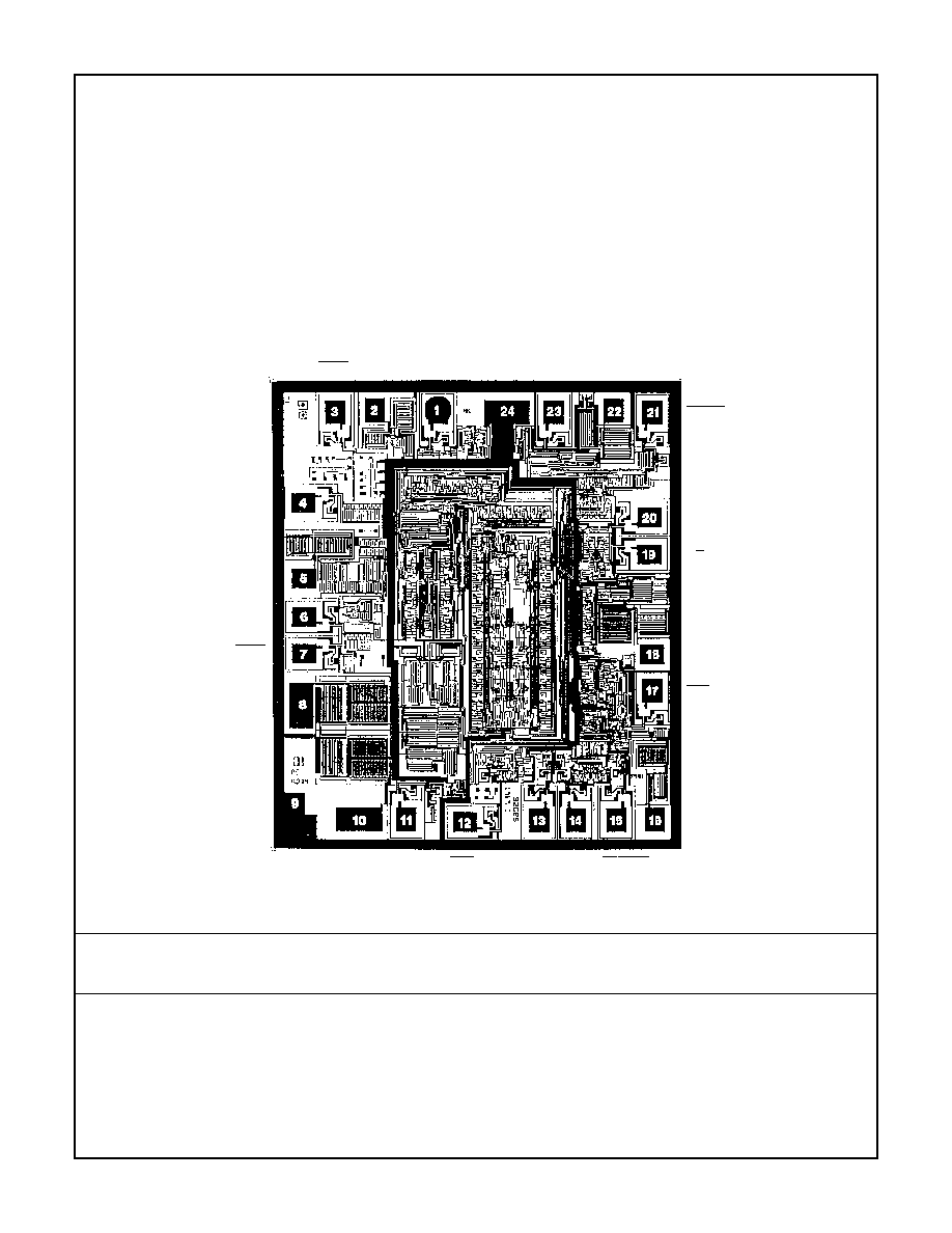
Metallization Mask Layout
82C85
AEN1 PCLK
CSYNC
V
CC
X1
X2
ASYNC
EFI
F/C
OSC
RES
RESET
S2/STOP
S1
S0
SLO/FST
START
CLK50
GND
CLK
AEN2
RDY2
READY
RDY1