 | –≠–ª–µ–∫—Ç—Ä–æ–Ω–Ω—ã–π –∫–æ–º–ø–æ–Ω–µ–Ω—Ç: 82C87H-5 | –°–∫–∞—á–∞—Ç—å:  PDF PDF  ZIP ZIP |

325
TM
82C87H
CMOS Octal Inverting Bus Transceiver
FN2978.1
March 1997
Features
∑ Full Eight Bit Bi-Directional Bus Interface
∑ Industry Standard 8287 Compatible Pinout
∑ High Drive Capability
- B Side I
OL
. . . . . . . . . . . . . . . . . . . . . . . . . . . . . . 20mA
- A Side I
OL
. . . . . . . . . . . . . . . . . . . . . . . . . . . . . . 12mA
∑ Three-State Inverting Outputs
∑ Propagation Delay . . . . . . . . . . . . . . . . . . . . . 35ns Max.
∑ Gated Inputs
- Reduce Operating Power
- Eliminate the Need for Pull-Up Resistors
∑ Single 5V Power Supply
∑ Low Power Operation . . . . . . . . . . . . . . . ICCSB = 10
µ
A
∑ Operating Temperature Range
- C82C87H . . . . . . . . . . . . . . . . . . . . . . . . . 0
o
C to +70
o
C
- I82C87H . . . . . . . . . . . . . . . . . . . . . . . . -40
o
C to +85
o
C
- M82C87H . . . . . . . . . . . . . . . . . . . . . . -55
o
C to +125
o
C
Description
The Intersil 82C87H is a high performance CMOS Octal
Transceiver manufactured using a self-aligned silicon gate
CMOS process (Scaled SAJI IV). The 82C87H provides a full
eight-bit bi-directional bus interface in a 20 pin package. The
Transmit (T) control determines the data direction. The active
low output enable (OE) permits simple interface to the
80C86, 80C88 and other microprocessors. The 82C87H has
gated inputs, eliminating the need for pull-up/pull-down resis-
tors and reducing overall system operating power dissipation.
The 82C87H provides inverted data at the outputs.
Ordering Information
PART NUMBERS
PACK-
AGE
TEMP. RANGE
PKG.
NO.
5MHz
8MHz
CP82C87H-5
CP82C87H 20 Ld
PDIP
0
o
C to +70
o
C E20.3
IP82C87H-5
IP82C87H
-40
o
C to +85
o
C E20.3
CS82C87H-5
CS82C87H 20 Ld
PLCC
0
o
C to +70
o
C N20.35
IS82C87H-5
IS82C87H
-40
o
C to +85
o
C N20.35
CD82C87H-5
CD82C87H 20 Ld
CERDIP
0
o
C to +70
o
C F20.3
ID82C87H-5
ID82C87H
-40
o
C to +85
o
C F20.3
MD82C87H-5/B
-
-55
o
C to
+125
o
C
F20.3
5962-
8757702RA
-
SMD #
F20.3
MR82C87H-5/B
-
20 Pad
CLCC
-55
o
C to
+125
o
C
J20.A
5962-
87577022A
-
SMD #
J20.A
CAUTION: These devices are sensitive to electrostatic discharge; follow proper IC Handling Procedures.
1-888-INTERSIL or 321-724-7143
|
Intersil (and design) is a trademark of Intersil Americas Inc.
Copyright © Intersil Americas Inc. 2002. All Rights Reserved

326
Pinouts
82C87H (PDIP, CERDIP)
TOP VIEW
82C87H (PLCC, CLCC)
TOP VIEW
11
12
13
14
15
16
17
18
20
19
10
9
8
7
6
5
4
3
2
1
A0
A1
A2
A3
A4
A5
A7
A6
OE
GND
V
CC
B1
B2
B3
B0
B4
B5
B6
B7
T
19
3
2
20
1
15
16
17
18
14
9
10
11
12
13
4
5
6
7
8
A4
A5
A6
A7
A3
OE
GN
D
T
B7
B6
B2
B3
B4
B5
B1
A2
A1
A0
V
CC
B0
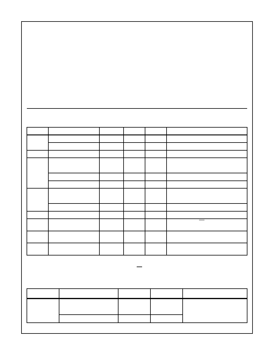
TRUTH TABLE
T
OE
A
B
X
H
Hi-Z
Hi-Z
H
L
I
O
L
L
O
I
H
= Logic One
L
= Logic Zero
I =
Input
Mode
O =
Output
Mode
X =
Don't
Care
Hi-Z = High Impedance
PIN NAMES
PIN
DESCRIPTION
A
0
-A
7
Local Bus Data I/O Pins
B
0
-B
7
System Bus Data I/O Pins
T
Transmit Control Input
OE
Active Low Output Enable
82C87H
82C87H

327
82C87H
Functional Diagram
Gated Inputs
During normal system operation of a latch, signals on the
bus at the device inputs will become high impedance or
make transitions unrelated to the operation of the latch.
These unrelated input transitions switch the input circuitry
and typically cause an increase in power dissipation in
CMOS devices by creating a low resistance path between
V
CC
and GND when the signal is at or near the input switch-
ing threshold. Additionally, if the driving signal becomes high
impedance ("float" condition), it could create an indetermi-
nate logic state at the inputs and cause a disruption in
device operation.
The Intersil 82C8X series of bus drivers eliminates these
conditions by turning off data inputs when data is latched
(STB = logic zero for the 82C82/83H) and when the device is
disabled (OE = logic one for the 82C87H/87H). These gated
inputs disconnect the input circuitry from the V
CC
and ground
power supply pins by turning off the upper P-Channel and
lower N-Channel (See Figures 1 and 2). No current flow from
V
CC
to GND occurs during input transitions and invalid logic
states from floating inputs are not transmitted. The next
stage is held to a valid logic level internal to the device.
D.C. input voltage levels can also cause an increase in ICC
if these input levels approach the minimum V
IH
or maximum
V
IL
conditions. This is due to the operation of the input cir-
cuitry in its linear operating region (partially conducting
state). The 82C8X series gated inputs mean that this condi-
tion will occur only during the time the device is in the trans-
parent mode (STB = logic one). ICC remains below the
maximum ICC standby specification of 10
µ
A during the time
inputs are disabled, thereby greatly reducing the average
power dissipation of the 82C8X series devices.
Decoupling Capacitors
The transient current required to charge and discharge the
300pF load capacitance specified in the 82C86H/87H data
sheet is determined by:
Assuming that all outputs change state at the same time and
that dv/dt is constant;
where tR = 20ns, V
CC
= 5.0V, C
L
= 300pF on each eight out-
puts.
This current spike may cause a large negative voltage spike on
V
CC
which could cause improper operation of the device. To fil-
ter out this noise, it is recommended that a 0.1
µ
F ceramic disc
capacitor be placed between V
CC
and GND at each device,
with placement being as near to the device as possible.
T
B7
B6
B5
B4
B3
B2
B1
B0
A0
A1
A2
A3
A4
A5
A6
A7
OE
I
C
L
dv dt
/
(
)
=
(EQ. 4)
I
C
L
VCC 80%
◊
(
)
tR tF
/
-------------------------------------
=
(EQ. 5)
I
80 300 10
12
≠
◊
◊
(
)
5.0V 0.8
◊
(
)
20 10
9
≠
◊
(
)
/
◊
=
480mA
=
(EQ. 6)
STB
DATA IN
V
CC
P
N
V
CC
INTERNAL
DATA
P
P
N
N
FIGURE 3. 82C82/83H
DATA IN
INTERNAL
DATA
V
CC
V
CC
N
N
P
P
P
N
OE
FIGURE 4. 82C86H/87H GATED INPUTS
82C87H
328
Absolute Maximum Ratings
Thermal Information
Supply Voltage . . . . . . . . . . . . . . . . . . . . . . . . . . . . . . . . . . . . . +8.0V
Input, Output or I/O Voltage . . . . . . . . . . . . GND -0.5V to V
CC
+0.5V
ESD Classification . . . . . . . . . . . . . . . . . . . . . . . . . . . . . . . . Class 1
Operating Conditions
Operating Voltage Range . . . . . . . . . . . . . . . . . . . . . +4.5V to +5.5V
Operating Temperature Range
C82C87H . . . . . . . . . . . . . . . . . . . . . . . . . . . . . . . . . 0
o
C to +70
o
C
I82C87H . . . . . . . . . . . . . . . . . . . . . . . . . . . . . . . . -40
o
C to +85
o
C
M82C87H . . . . . . . . . . . . . . . . . . . . . . . . . . . . . . -55
o
C to +125
o
C
Thermal Resistance (Typical)
JA
(
o
C/W)
JC
(
o
C/W)
CERDIP Package . . . . . . . . . . . . . . . .
70
16
CLCC Package . . . . . . . . . . . . . . . . . .
80
20
PDIP Package . . . . . . . . . . . . . . . . . . .
75
N/A
PLCC Package . . . . . . . . . . . . . . . . . .
75
N/A
Storage Temperature Range . . . . . . . . . . . . . . . . . -65
o
C to +150
o
C
Maximum Junction Temperature Hermetic Package . . . . . . +175
o
C
Maximum Junction Temperature Plastic Package . . . . . . . . +150
o
C
Maximum Lead Temperature (Soldering 10s). . . . . . . . . . . . +300
o
C
(PLCC - Lead Tips Only)
Die Characteristics
Gate Count . . . . . . . . . . . . . . . . . . . . . . . . . . . . . . . . . . . . 265 Gates
CAUTION: Stresses above those listed in "Absolute Maximum Ratings" may cause permanent damage to the device. This is a stress only rating and operation
of the device at these or any other conditions above those indicated in the operational sections of this specification is not implied.
DC Electrical Specifications
V
CC
= 5.0V
±
10%; T
A
= 0
o
C to +70
o
C (C82C87H);
T
A
= -40
o
C to +85
o
C (I82C87H);
T
A
= -55
o
C to +125
o
C (M82C87H)
SYMBOL
PARAMETER
MIN
MAX
UNITS
TEST CONDITIONS
V
IH
Logical One
2.0
-
V
C82C87H, I82C87H
Input Voltage
2.2
-
V
M82C87H (Note 1)
V
IL
Logical Zero Input Voltage
-
0.8
V
V
OH
Logical One Output Voltage
B Outputs
3.0
-
V
I
OH
= -8mA
A Outputs
3.0
-
V
I
OH
= -4mA
A or B Outputs
V
CC
-0.4
-
V
I
OH
= -100
µ
A
V
OL
Logical Zero Output Voltage
B Outputs
-
0.45
V
I
OL
= 20mA
A Outputs
-
0.45
V
I
OL
= 12mA
I
I
Input Leakage Current
-10.0
10.0
µ
A
V
IN
= GND or V
CC
DIP Pins 9, 11
IO
Output Leakage Current
-10.0
10.0
µ
A
VO = GND or V
CC
, OE S S
V
CC
-0.5V
DIP Pins 1 - 8, 12 - 19
ICCSB
Standby Power Supply
Current
-
10
µ
A
V
IN
= V
CC
or GND, V
CC
= 5.5V, Outputs Open
ICCOP
Operating Power Supply
Current
-
1
mA/MHz
T
A
= +25
o
C, Typical (See Note 2)
NOTES:
1. V
IH
is measured by applying a pulse of magnitude = V
IH(MIN)
to one data input at a time and checking the corresponding device output
for a valid logical "1" during valid input high time. Control pins (T, OE) are tested separately with all device data input pins at V
CC
-0.4.
2. Typical ICCOP = 1mA/MHz of read/ cycle time. (Example: 1.0
µ
s read/write cycle time = 1mA).
Capacitance
T
A
= +25
o
C
SYMBOL
PARAMETER
TYPICAL
UNITS
TEST CONDITIONS
CIN
Input Capacitance
B Inputs
18
pF
Freq = 1MHz, all measurements are
referenced to device GND
A Inputs
14
pF
82C87H
82C87H
329
Timing Waveform
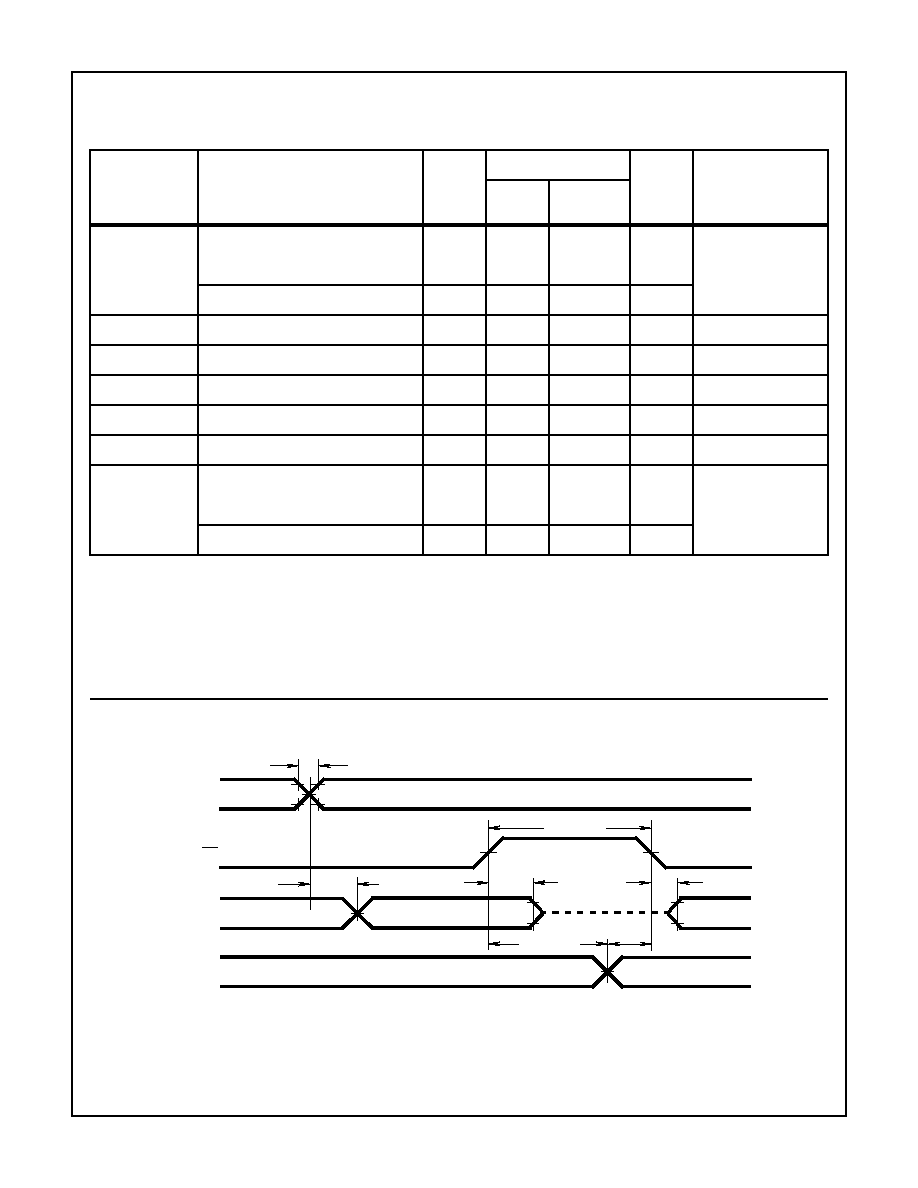
AC Electrical Specifications
V
CC
= 5.0V
±
10%;
T
A
= 0
o
C to +70
o
C (C82C87H);
Freq = 1MHz
T
A
= -40
o
C to +85
o
C (I82C87H);
T
A
= -55
o
C to +125
o
C (M82C87H)
SYMBOL
PARAMETER
MIN
NOTE 4
UNITS
TEST CONDITIONS
82C87H
MAX
82C87H-5
MAX
(1)
TIVOV
Input to Output Delay
Notes 1, 2
Inverting
5
30
35
ns
Non-Inverting
5
32
35
ns
(2)
TEHTV
Transmit/Receive Hold Time
5
-
-
ns
Notes 1, 2
(3)
TTVEL
Transmit/Receive Setup Time
10
-
-
ns
Notes 1, 2
(4)
TEHOZ
Output Disable Time
5
30
35
ns
Notes 1, 2
(5)
TELOV
Output Enable Time
10
50
65
ns
Notes 1, 2
(6)
TR, TF
Input Rise/Fall Times
-
20
20
ns
Notes 1, 2
(7)
TEHEL
Minimum Output Enable High Time
Note 3
82C87H
30
-
-
ns
82C87H-5
35
-
-
ns
NOTES:
1. All AC parameters tested as per test circuits and definitions in timing waveforms and test load circuits. Input rise and fall times are driven
at 1ns/V.
2. Input test signals must switch between V
IL
- 0.4V and V
IH
+0.4V.
3. A system limitation only when changing direction. Not a measured parameter.
4. 82C87H is available in commercial and industrial temperature ranges only. 82C87H-5 is available in commercial, industrial and military
temperature ranges.
INPUTS
TR, TF (6)
2.0V
0.8V
V
OH
-0.1V
TELOV (5)
V
OL
+0.1V
TTVEL (3)
3.0V
0.45V
OUTPUTS
T
TEHEL (7)
TIVOV
(1)
TEHOZ
(4)
TEHTV (2)
OE
82C87H
82C87H
330
Test Load Circuits
A SIDE OUTPUTS
TIVOV LOAD CIRCUIT
TELOV OUTPUT HIGH
ENABLE LOAD CIRCUIT
TELOV OUTPUT LOW
ENABLE LOAD CIRCUIT
TEHOZ OUTPUT LOW/HIGH
DISABLE LOAD CIRCUIT
B SIDE OUTPUTS
TIVOV LOAD CIRCUIT
TELOV OUTPUT HIGH
ENABLE LOAD CIRCUIT
TELOV OUTPUT LOW
ENABLE LOAD CIRCUIT
TEHOZ OUTPUT LOW/HIGH
DISABLE LOAD CIRCUIT
NOTE: Includes jig and stray capacitance.
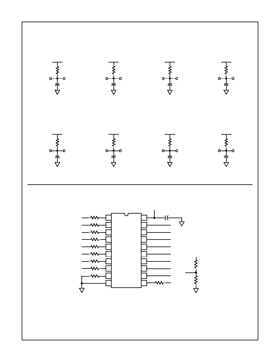
Burn-In Circuits
MD82C87H CERDIP
OUTPUT
TEST
POINT
2.36V
100pF
160
(SEE NOTE)
OUTPUT
TEST
POINT
1.5V
100pF
375
(SEE NOTE)
OUTPUT
TEST
POINT
1.5V
100pF
91
(SEE NOTE)
OUTPUT
TEST
POINT
2.36V
50pF
160
(SEE NOTE)
OUTPUT
TEST
POINT
2.27V
300pF
91
(SEE NOTE)
OUTPUT
TEST
POINT
1.5V
300pF
180
(SEE NOTE)
OUTPUT
TEST
POINT
1.5V
300pF
51
(SEE NOTE)
OUTPUT
TEST
POINT
2.27V
50pF
91
(SEE NOTE)
10
9
8
7
6
5
4
3
2
1
11
12
13
14
15
16
17
18
19
20
V
CC
F2
R1
F2
F2
F2
F2
F2
F2
F2
A
A
A
A
A
A
A
A
R1
V
CC
C1
R2
V
CC
A
R1
R1
R1
R1
R1
R1
R1
R1
R3
82C87H
82C87H

331
MR82C87H CLCC
NOTES:
1. V
CC
= 5.5V
±
0.5V, GND = 0V
2. V
IH
= 4.5V
±
10%
3. V
IL
= -0.2V to 0.4V
4. R1 = 47k
±
5%
5. R2 = 2.4k
±
5%
6. R3 = 1.5k
±
5%
7. R4 = 1k
±
5%
8. R5 = 5k
±
5%
9. C1 = 0.01
µ
F minimum
10. F0 = 100kHz
±
10%
11. F1 = F0/2, F2 = F1/2, F3 = F2/2
Burn-In Circuits
(Continued)
4
5
6
7
8
9
10
11
12
13
15
14
18
17
16
V
CC
C1
F2
F2
R5
F2
R5 R5
F3
R5
F1
F0
F3
F2
F2
F2
F2
F2
R5
R5
R5
R5
R5
F3
F3
F3
F3
F3
R5
R5
R5
R5
R5
R4
R4
R5
R5
F3
3
2
1
20
19
82C87H
82C87H
332
All Intersil U.S. products are manufactured, assembled and tested utilizing ISO9000 quality systems.
Intersil Corporation's quality certifications can be viewed at www.intersil.com/design/quality
Intersil products are sold by description only. Intersil Corporation reserves the right to make changes in circuit design, software and/or specifications at any time without
notice. Accordingly, the reader is cautioned to verify that data sheets are current before placing orders. Information furnished by Intersil is believed to be accurate and
reliable. However, no responsibility is assumed by Intersil or its subsidiaries for its use; nor for any infringements of patents or other rights of third parties which may result
from its use. No license is granted by implication or otherwise under any patent or patent rights of Intersil or its subsidiaries.
For information regarding Intersil Corporation and its products, see www.intersil.com
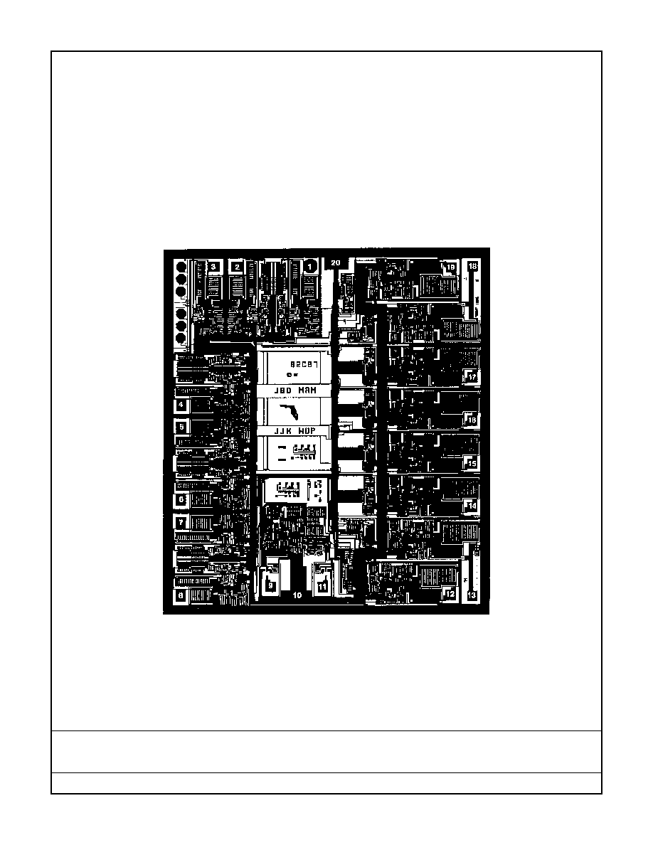
Die Characteristics
DIE DIMENSIONS:
138.6 x 155.5 x 19
±
1mils
METALLIZATION:
Type: Si - Al
Thickness: 11k
≈
±
1k
≈
GLASSIVATION:
Type: SiO
2
Thickness: 8k
≈
±
1k
≈
WORST CASE CURRENT DENSITY:
1.47 x 10
5
A/cm
2
Metallization Mask Layout
82C87H
A2
A1
A0
V
CC
B0
B1
B2
B3
B4
B5
B6
B7
T
GND
OE
A7
A6
A5
A4
A3
82C87H
82C87H