 | –≠–ª–µ–∫—Ç—Ä–æ–Ω–Ω—ã–π –∫–æ–º–ø–æ–Ω–µ–Ω—Ç: 8403601ZA | –°–∫–∞—á–∞—Ç—å:  PDF PDF  ZIP ZIP |
6-1
March 1997
HM-6516
2K x 8 CMOS RAM
Features
∑ Low Power Standby . . . . . . . . . . . . . . . . . . . 275
µ
W Max
∑ Low Power Operation . . . . . . . . . . . . . 55mW/MHz Max
∑ Fast Access Time. . . . . . . . . . . . . . . . . . 120/200ns Max
∑ Industry Standard Pinout
∑ Single Supply . . . . . . . . . . . . . . . . . . . . . . . . . . 5.0V V
CC
∑ TTL Compatible
∑ Static Memory Cells
∑ High Output Drive
∑ On-Chip Address Latches
∑ Easy Microprocessor Interfacing
Description
The HM-6516 is a CMOS 2048 x 8 Static Random Access
Memory. Extremely low power operation is achieved by the
use of complementary MOS design techniques. This low
power is further enhanced by the use of synchronous circuit
techniques that keep the active (operating) power low, which
also gives fast access times. The pinout of the HM-6516 is
the popular 24 pin, 8-bit wide JEDEC standard, which allows
easy memory board layouts, flexible enough to accommo-
date a variety of PROMs, RAMS, EPROMs, and ROMs.
The HM-6516 is ideally suited for use in microprocessor
based systems. The byte wide organization simplifies the
memory array design, and keeps operating power down to a
minimum, because only one device is enabled at a time. The
address latches allow very simple interfacing to recent gen-
eration microprocessors which employ a multiplexed
address/data bus. The convenient output enable control also
simplifies multiplexed bus interfacing by allowing the data
outputs to be controlled independent of the chip enable.
Ordering Information
120ns
200ns
TEMP. RANGE
PACKAGE
PKG. NO.
HM1-6516B-9
HM1-6516-9
-40
o
C to +85
o
C
CERDIP
F24.6
-
29102BJA
-55
o
C to +125
o
C
JAN#
F24.6
8403607JA
8403601JA
-55
o
C to +125
o
C
SMD#
F24.6
-
HM4-6516-9
-40
o
C to +85
o
C
CLCC
J32.A
8403607ZA
8403601ZA
-55
o
C to +125
o
C
SMD#
J32.A
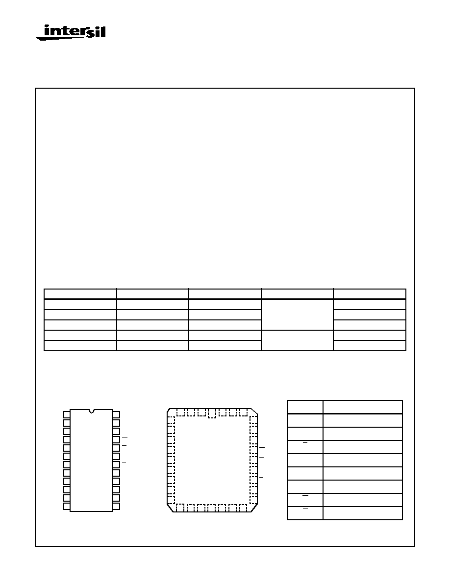
Pinouts
HM-6516
(CERDIP)
TOP VIEW
HM-6516
(CLCC)
TOP VIEW
1
2
3
4
5
6
7
8
9
10
11
12
16
17
18
19
20
21
22
23
24
15
14
13
A7
A6
A5
A4
A3
A2
A1
A0
DQ0
DQ1
DQ2
GND
V
CC
A9
W
G
A10
DQ7
DQ5
DQ4
DQ3
A8
E
DQ6
5
6
7
8
11
10
9
13
12
27
28
29
26
25
24
23
22
21
3
2
1
4
32 31
30
16
17 18
19
20
14 15
A6
A5
A4
A3
A2
A1
A0
NC
DQ0
DQ1
DQ2
GND
NC
DQ3
DQ4
DQ5
V
CC
NC
NC
A7
NC
NC
NC
A8
A9
NC
G
A10
E
DQ7
DQ6
W
PIN
DESCRIPTION
NC
No Connect
A0 - A10
Address Inputs
E
Chip Enable/Power Down
V
SS
/GND
Ground
DQ0 - DQ7 Data In/Data Out
V
CC
Power (+5V)
W
Write Enable
G
Output Enable
File Number
2998.1
CAUTION: These devices are sensitive to electrostatic discharge; follow proper IC Handling Procedures.
http://www.intersil.com or 407-727-9207
|
Copyright
©
Intersil Corporation 1999
6-2
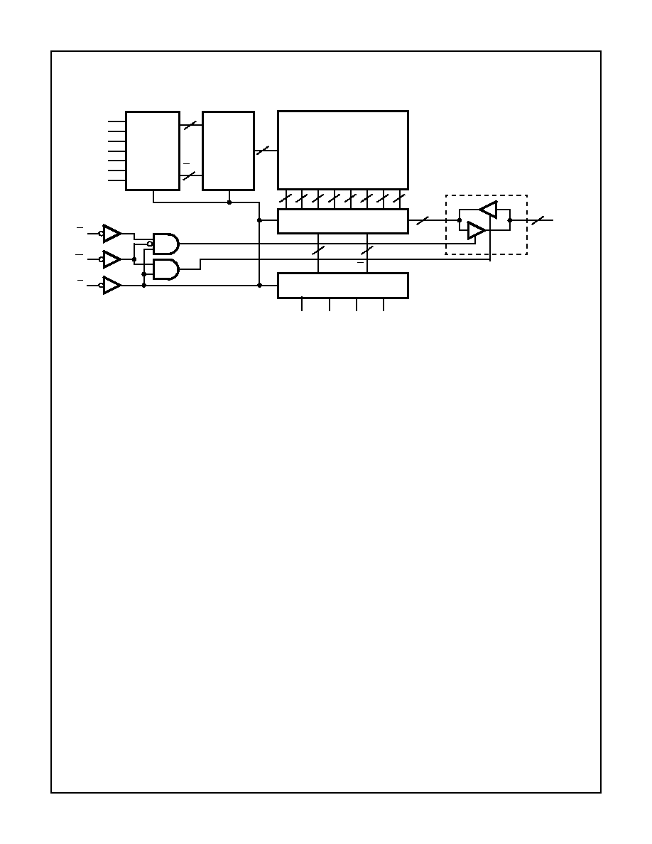
Functional Diagram
A10
A9
A8
A7
A6
A5
A4
128
A
7
7
4
4
A
A3
A2
A1
A0
L
L
G
G
8
1 OF 8
8
A
A
GATED COLUMN
DECODER
LATCHED ADDRESS
REGISTER
LATCHED
ADDRESS
REGISTER
GATED
ROW
DECODER
128 x 128
MATRIX
A
E
W
G
A
16
16
16
16
16
16
16
16
DQ0
THRU
DQ7
HM-6516

6-3
Absolute Maximum Ratings
Thermal Information
Supply Voltage . . . . . . . . . . . . . . . . . . . . . . . . . . . . . . . . . . . . . +7.0V
Input or Output Voltage Applied for all Grades . . . . . . .GND -0.3V to
V
CC
+0.3V
ESD Classification . . . . . . . . . . . . . . . . . . . . . . . . . . . . . . . . Class 1
Operating Conditions
Operating Voltage Range . . . . . . . . . . . . . . . . . . . . . +4.5V to +5.5V
Operating Temperature Ranges:
HM-6516B-9, HM-6516-9 . . . . . . . . . . . . . . . . . . . -40
o
C to +85
o
C
Thermal Resistance
JA
JC
CERDIP Package . . . . . . . . . . . . . . . .
48
o
C/W
8
o
C/W
CLCC Package . . . . . . . . . . . . . . . . . .
66
o
C/W
12
o
C/W
Maximum Storage Temperature Range . . . . . . . . .-65
o
C to +150
o
C
Maximum Junction Temperature . . . . . . . . . . . . . . . . . . . . . . +175
o
C
Maximum Lead Temperature (Soldering 10s) . . . . . . . . . . . . +300
o
C
Die Characteristics
Gate Count . . . . . . . . . . . . . . . . . . . . . . . . . . . . . . . . . . 25953 Gates
CAUTION: Stresses above those listed in "Absolute Maximum Ratings" may cause permanent damage to the device. This is a stress only rating and operation
of the device at these or any other conditions above those indicated in the operational sections of this specification is not implied.
DC Electrical Specifications
V
CC
= 5V
±
10%; T
A
= -40
o
C to +85
o
C (HM-6516B-9, HM-6516-9)
SYMBOL
PARAMETER
LIMITS
UNITS
TEST CONDITIONS
MIN
MAX
ICCSB
Standby Supply Current
-
50
µ
A
IO = 0mA, VI = V
CC
or GND,
V
CC
= 5.5V, HM-6516B-9
-
100
µ
A
IO = 0mA, VI = V
CC
or GND,
HM-6516-9
ICCOP
Operating Supply Current (Note 1)
-
10
mA
f = 1MHz, IO = 0mA, G = V
CC
, V
CC
=
5.5V, VI = V
CC
or GND
ICCDR
Data Retention Supply Current
-
25
µ
A
V
CC
= 2.0V, IO = 0mA, VI = V
CC
or
GND, E = V
CC
, HM-6516B-9
-
50
µ
A
V
CC
= 2.0V, IO = 0mA, VI = V
CC
or
GND, E = V
CC
, HM-6516-9
VCCDR
Data Retention Supply Voltage
2.0
-
V
II
Input Leakage Current
-1.0
+1.0
µ
A
VI = V
CC
or GND, V
CC
= 5.5V
IIOZ
Input/Output Leakage Current
-1.0
+1.0
µ
A
VIO = V
CC
or GND, V
CC
= 5.5V
V
IL
Input Low Voltage
-0.3
0.8
V
V
CC
= 4.5V
V
IH
Input High Voltage
2.4
V
CC
+0.3
V
V
CC
= 5.5V
VOL
Output Low Voltage
-
0.4
V
IO = 3.2mA, V
CC
= 4.5V
VOH1
Output High Voltage
2.4
-
V
IO = -1.0mA, V
CC
= 4.5V
VOH2
Output High Voltage (Note 2)
V
CC
-0.4
-
V
IO = -100
µ
A, V
CC
= 4.5V
Capacitance
T
A
= +25
o
C
SYMBOL
PARAMETER
MAX
UNITS
TEST CONDITIONS
CI
Input Capacitance (Note 2)
8
pF
f = 1MHz, All measurements are
referenced to device GND
CIO
Input/Output Capacitance (Note 2)
10
pF
NOTES:
1. Typical derating 5mA/MHz increase in ICCOP.
2. Tested at initial design and after major design changes.
HM-6516

6-4
AC Electrical Specifications
V
CC
= 5V
±
10%; T
A
= -40
o
C to +85
o
C (HM-6516B-9, HM-6516-9)
SYMBOL
PARAMETER
LIMITS
UNITS
TEST
CONDITIONS
HM-6516B-9
HM-6516-9
MIN
MAX
MIN
MAX
(1)
TELQV
Chip Enable Access Time
-
120
-
200
ns
(Notes 1, 3)
(2)
TAVQV
Address Access Time
-
120
-
200
ns
(Notes 1, 3, 4)
(3)
TELQX
Chip Enable Output Enable Time
10
-
10
-
ns
(Notes 2, 3)
(4)
TWLQZ
Write Enable Output Disable Time
-
50
-
80
ns
(Notes 2, 3)
(5)
TEHQZ
Chip Enable Output Disable Time
-
50
-
80
ns
(Notes 2, 3)
(6)
TGLQV
Output Enable Output Valid Time
-
80
-
80
ns
(Notes 1, 3)
(7)
TGLQX
Output Enable Output Enable Time
10
-
10
-
ns
(Notes 2, 3)
(8)
TGHQZ
Output Enable Output DisableTime
-
50
-
80
ns
(Notes 2, 3)
(9)
TELEH
Chip Enable Pulse Negative Width
120
-
200
-
ns
(Notes 1, 3)
(10)
TEHEL
Chip Enable Pulse Positive Width
50
-
80
-
ns
(Notes 1, 3)
(11)
TAVEL
Address Setup Time
0
-
0
-
ns
(Notes 1, 3)
(12)
TELAX
Address Hold Time
30
-
50
-
ns
(Notes 1, 3)
(13)
TWLWH
Write Enable Pulse Width
120
-
200
-
ns
(Notes 1, 3)
(14)
TWLEH
Write Enable Pulse Setup Time
120
-
200
-
ns
(Notes 1, 3)
(15)
TELWH
Write Enable Pulse Hold Time
120
-
200
-
ns
(Notes 1, 3)
(16)
TDVWH
Data Setup Time
50
-
80
-
ns
(Notes 1, 3)
(17)
TWHDX
Data Hold Time
10
-
10
-
ns
(Notes 1, 3)
(18)
TELEL
Read or Write Cycle Time
170
-
280
-
ns
(Notes 1, 3)
NOTES:
1. Input pulse levels: 0.8V to V
CC
- 2.0V; Input rise and fall times: 5ns (max); Input and output timing reference level: 1.5V; Output load:
1 TTL gate equivalent, C
L
= 50pF (min) - for C
L
greater than 50pF, access time is derated by 0.15ns per pF.
2. Tested at initial design and after major design changes.
3. V
CC
= 4.5V and 5.5V.
4. TAVQV = TELQV + TAVEL.
HM-6516
6-5
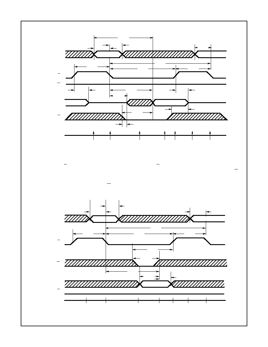
Timing Waveforms
The address information is latched in the on-chip registers
on the falling edge of E (T = 0), minimum address setup and
hold time requirements must be met. After the required hold
time, the addresses may change state without affecting
device operation. During time (T = 1), the outputs become
enabled but data is not valid until time (T = 2), W must
remain high throughout the read cycle. After the data has
been read, E may return high (T = 3). This will force the out-
put buffers into a high impedance mode at time (T = 4). G is
used to disable the output buffers when in a logical "1" state
(T = -1, 0, 3, 4, 5). After (T = 4) time, the memory is ready for
the next cycle.
Timing Waveforms
(Continued)
HIGH
NEXT
(11)
TAVEL
(12)
TELAX
ADD
(5)
TEHQZ
VALID DATA OUT
(5)
TEHQZ
(8)
TGHQZ
(7)
TGLQX
A
E
W
DQ
G
TIME
REFERENCE
-1
0
1
2
3
4
5
TAVQV
(2)
(11)
TAVEL
(18)
TELEL
(9)
TELEH
(10)
TEHEL
(10)
TEHEL
TELQV
(1)
TELQX
(3)
TGLQV
(6)
FIGURE 1. READ CYCLE
VALID ADD
(11)
TAVEL
(12)
TELAX
(11)
TAVEL
(17)
TWHDX
HIGH
VALID DATA IN
A
E
W
DQ
G
TIME
REFERENCE
-1
0
1
2
3
4
5
VALID ADD
NEXT ADD
(18)
TELEL
(10)
TEHEL
(10)
TEHEL
(9)
TELEH
(13)
TWLWH
(14)
TWLEH
(16)
TDVWH
FIGURE 2. WRITE CYCLE
(15)
TELWH
HM-6516
6-6
All Intersil semiconductor products are manufactured, assembled and tested under ISO9000 quality systems certification.
Intersil products are sold by description only. Intersil Corporation reserves the right to make changes in circuit design and/or specifications at any time without
notice. Accordingly, the reader is cautioned to verify that data sheets are current before placing orders. Information furnished by Intersil is believed to be accurate
and reliable. However, no responsibility is assumed by Intersil or its subsidiaries for its use; nor for any infringements of patents or other rights of third parties which
may result from its use. No license is granted by implication or otherwise under any patent or patent rights of Intersil or its subsidiaries.
For information regarding Intersil Corporation and its products, see web site http://www.intersil.com
Sales Office Headquarters
NORTH AMERICA
Intersil Corporation
P. O. Box 883, Mail Stop 53-204
Melbourne, FL 32902
TEL: (407) 724-7000
FAX: (407) 724-7240
EUROPE
Intersil SA
Mercure Center
100, Rue de la Fusee
1130 Brussels, Belgium
TEL: (32) 2.724.2111
FAX: (32) 2.724.22.05
ASIA
Intersil (Taiwan) Ltd.
Taiwan Limited
7F-6, No. 101 Fu Hsing North Road
Taipei, Taiwan
Republic of China
TEL: (886) 2 2716 9310
FAX: (886) 2 2715 3029
The write cycle is initiated on the falling edge of E (T = 0),
which latches the address information in the on-chip
registers. If a write cycle is to be performed where the output
is not to become active, G can be held high (inactive).
TDVWH and TWHDX must be met for proper device opera-
tion regardless of G. If E and G fall before W falls (read
mode), a possible bus conflict may exist. If E rises before W
rises, reference data setup and hold times to the E rising
edge. The write operation is terminated by the first rising edge
of W (T = 2) or E (T = 3). After the minimum E high time
(TEHEL), the next cycle may begin. If a series of consecutive
write cycles are to be performed, the W line may be held low
until all desired locations have been written. In this case, data
setup and hold times must be referenced to the rising of E.
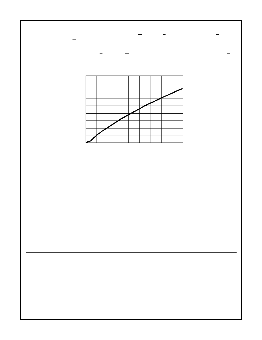
Typical Performance Curve
-55
-35
-15
5
25
45
65
85
105
125
-12
-11
-10
-9
-8
-7
-6
-5
-4
-3
V
CC
= 2.0V
LOG (I
CC
/(1A))
FIGURE 3. TYPICAL ICCDR vs T
A
HM-6516