
1
Æ
CAUTION: These devices are sensitive to electrostatic discharge; follow proper IC Handling Procedures.
1-888-INTERSIL or 321-724-7143
|
Intersil (and design) is a registered trademark of Intersil Americas Inc.
Copyright © Intersil Americas Inc. 2003. All Rights Reserved.
All other trademarks mentioned are the property of their respective owners.
General Purpose NPN Transistor Array
The CA3086 consists of five general-purpose silicon NPN
transistors on a common monolithic substrate. Two of the
transistors are internally connected to form a differentially
connected pair.
The transistors of the CA3086 are well suited to a wide
variety of applications in low-power systems at frequencies
from DC to 120MHz. They may be used as discrete
transistors in conventional circuits. However, they also
provide the very significant inherent advantages unique to
integrated circuits, such as compactness, ease of physical
handling and thermal matching.
Applications
∑ Power Applications from DC to 120MHz
∑ General-Purpose Use in Signal Processing Systems
Operating in the DC to 190MHz Range
∑ Temperature Compensated Amplifiers
∑ See Application Note, AN5296 "Application of the CA3018
Integrated-Circuit Transistor Array" for Suggested
Applications
Pinout
CA3086 (PDIP, SOIC)
TOP VIEW
Ordering Information
PART NUMBER
(BRAND)
TEMP.
RANGE (
o
C)
PACKAGE
PKG.
DWG. #
CA3086
-55 to 125
14 Ld PDIP
E14.3
CA3086M96
(3086)
-55 to 125
14 Ld SOIC Tape
and Reel
M14.15
SUBSTRATE
1
2
3
4
5
6
7
14
13
12
11
10
9
8
Q
1
Q
2
Q
5
Q
4
Q
3
FN483.5
CA3086
Data Sheet
August 2003

2
CA3086
Absolute Maximum Ratings
Thermal Information
The following ratings apply for each transistor in the device:
Collector-to-Emitter Voltage, V
CEO
. . . . . . . . . . . . . . . . . . . . .15V
Collector-to-Base Voltage, V
CBO
. . . . . . . . . . . . . . . . . . . . . . .20V
Collector-to-Substrate Voltage, V
CIO
(Note 1) . . . . . . . . . . . . .20V
Emitter-to-Base Voltage, V
EBO
. . . . . . . . . . . . . . . . . . . . . . . . .5V
Collector Current, I
C
. . . . . . . . . . . . . . . . . . . . . . . . . . . . . . . 50mA
Operating Conditions
Temperature Range. . . . . . . . . . . . . . . . . . . . . . . . . -55
o
C to 125
o
C
Thermal Resistance (Typical, Note 2)
JA
(
o
C/W)
JC
(
o
C/W)
PDIP Package . . . . . . . . . . . . . . . . . . .
110
N/A
SOIC Package . . . . . . . . . . . . . . . . . . .
130
N/A
Maximum Power Dissipation (Any one transistor) . . . . . . . . .300mW
Maximum Junction Temperature (Plastic Package) . . . . . . . .150
o
C
Maximum Storage Temperature Range . . . . . . . . . -65
o
C to 150
o
C
Maximum Lead Temperature (Soldering 10s) . . . . . . . . . . . . 300
o
C
(SOIC - Lead Tips Only)
CAUTION: Stresses above those listed in "Absolute Maximum Ratings" may cause permanent damage to the device. This is a stress only rating and operation of the
device at these or any other conditions above those indicated in the operational sections of this specification is not implied.
NOTES:
1. The collector of each transistor in the CA3086 is isolated from the substrate by an integral diode. The substrate (Terminal 13) must be connected
to the most negative point in the external circuit to maintain isolation between transistors and to provide for normal transistor action. To avoid
undesirable coupling between transistors, the substrate (Terminal 13) should be maintained at either DC or signal (AC) ground. A suitable
bypass capacitor can be used to establish a signal ground.
2.
JA
is measured with the component mounted on an evaluation PC board in free air.
Electrical Specifications
T
A
= 25
o
C, For Equipment Design
PARAMETER
SYMBOL
TEST CONDITIONS
MIN
TYP
MAX
UNITS
Collector-to-Base Breakdown Voltage
V
(BR)CBO
l
C
= 10
µ
A, I
E
= 0
20
60
-
V
Collector-to-Emitter Breakdown Voltage
V
(BR)CEO
I
C
= 1mA, I
B
= 0
15
24
-
V
Collector-to-Substrate Breakdown Voltage
V
(BR)ClO
I
C
= 10
µ
A, I
CI
= 0
20
60
-
V
Emitter-to-Base Breakdown Voltage
V
(BR)EBO
I
E
= 10
µ
A, I
C
= 0
5
7
-
V
Collector-Cutoff Current (Figure 1)
I
CBO
V
CB
= 10V, I
E
= 0,
-
0.002
100
nA
Collector-Cutoff Current (Figure 2)
I
CEO
V
CE
= 10V, I
B
= 0,
-
(Figure 2)
5
µ
A
DC Forward-Current Transfer Ratio (Figure 3)
h
FE
V
CE
= 3V, I
C
= 1mA
40
100
-
Electrical Specifications
T
A
= 25
o
C, Typical Values Intended Only for Design Guidance
PARAMETER
SYMBOL
TEST CONDITIONS
TYPICAL
VALUES
UNITS
DC Forward-Current Transfer Ratio
(Figure 3)
h
FE
V
CE
= 3V
I
C
= 10mA
100
I
C
= 10
µ
A
54
Base-to-Emitter Voltage (Figure 4)
V
BE
V
CE
= 3V
I
E
= 1 mA
0.715
V
I
E
= 10mA
0.800
V
V
BE
Temperature Coefficient (Figure 5)
V
BE
/
T V
CE
= 3V, l
C
= 1 mA
-1.9
mV/
o
C
Collector-to-Emitter
Saturation Voltage
V
CE SAT
I
B
= 1mA, I
C
= 10mA
0.23
V
Noise Figure (Low Frequency)
NF
f = 1kHz, V
CE
= 3V, I
C
= 100
µ
A,
R
S
= 1k
3.25
dB
3
CA3086
Low-Frequency, Small-Signal Equivalent-
Circuit Characteristics:
f = 1kHz,V
CE
= 3V, I
C
= 1mA
Forward Current-Transfer Ratio
(Figure 6)
h
FE
100
-
Short-Circuit Input Impedance
(Figure 6)
h
IE
3.5
k
Open-Circuit Output Impedance
(Figure 6)
h
OE
15.6
µ
S
Open-Circuit Reverse-Voltage
Transfer Ratio (Figure 6)
h
RE
1.8 X 10
-4
-
Admittance Characteristics:
f = 1MHz,V
CE
= 3V, l
C
= 1mA
Forward Transfer Admittance
(Figure 7)
y
FE
31 - j1.5
mS
Input Admittance (Figure 8)
y
IE
0.3 + j0.04
mS
Output Admittance (Figure 9)
y
OE
0.001 + j0.03
mS
Reverse Transfer Admittance
(Figure 10)
y
RE
See Figure 10
-
Gain-Bandwidth Product (Figure 11)
f
T
V
CE
= 3V, I
C
= 3mA
550
MHz
Emitter-to-Base Capacitance
C
EBO
V
EB
= 3V, I
E
= 0
0.6
pF
Collector-to-Base Capacitance
C
CBO
V
CB
= 3V, I
C
= 0
0.58
pF
Collector-to-Substrate Capacitance
C
ClO
V
C l
= 3V, I
C
= 0
2.8
pF
Electrical Specifications
T
A
= 25
o
C, Typical Values Intended Only for Design Guidance (Continued)
PARAMETER
SYMBOL
TEST CONDITIONS
TYPICAL
VALUES
UNITS
Typical Performance Curves
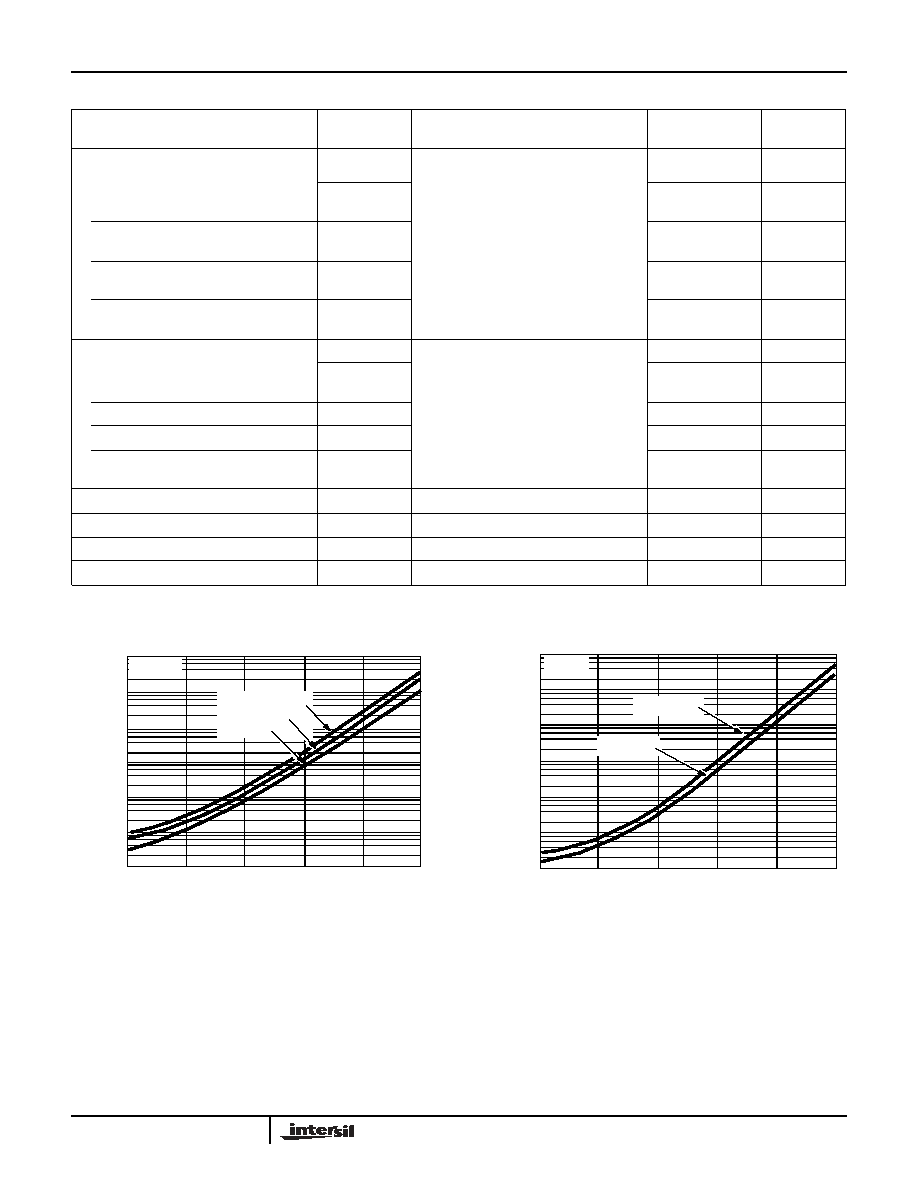
FIGURE 1. I
CBO
vs TEMPERATURE
FIGURE 2. I
CEO
vs TEMPERATURE
10
2
10
-1
10
1
10
-2
10
-3
10
-4
COLLECTOR
CUTOFF
CURRENT (nA)
0
25
50
75
100
125
TEMPERATURE (
o
C)
V
CB
= 15V
V
CB
= 10V
V
CB
= 5V
I
E
= 0
10
2
10
-1
10
1
10
-2
10
-3
COLLECTOR CUTOFF
CURRENT (nA)
0
25
50
75
100
125
TEMPERATURE (
o
C)
I
B
= 0
V
CE
= 10V
V
CE
= 5V
10
3

