8-33
May 1999
CA3126
TV Chroma Processor
CAUTION: These devices are sensitive to electrostatic discharge. Users should follow proper IC Handling Procedures.
Copyright
©
Harris Corporation 1999
File Number
860.5
Features
∑ Phase Locked Subcarrier Regeneration Utilizes
Sample-and-Hold Techniques
∑ Automatic Chrominance Control (ACC)/Killer Detector
Employs Sample-and-Hold Techniques
∑ Supplementary ACC with an Overload Detector to
Prevent Oversaturation of this Picture Tube
∑ Sinusoidal Subcarrier Output
∑ Keyed Chroma Output
∑ Emitter Follower Buffered Outputs for Low Output
Impedance
∑ Linear DC Saturation Control
Applications
∑ TV/CATV Receiver Circuits
∑ NTSC Color Decoder/Processor
∑ Computer Graphics Subcarrier Regenerator
∑ Timing Reference for Frame Grabbers
∑ DSP Clock Timing Reference Source
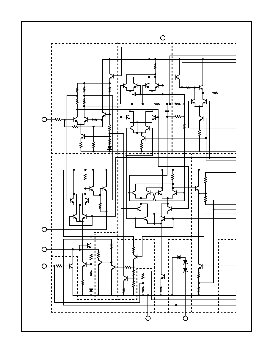
Description
The Harris CA3126 is a monolithic silicon integrated circuit
designed for TV chroma processing and is ideally suited for
NTSC color graphic applications that require subcarrier
regeneration of the color burst signal.
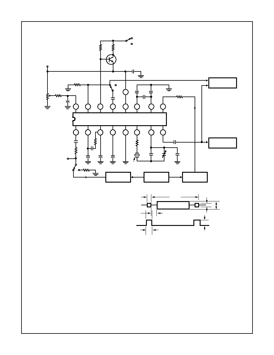
Pinouts
Part Number Information
PART NUMBER
TEMP.
RANGE (
o
C)
PACKAGE
PKG.
NO.
CA3126E
-40 to 85
16 Ld PDIP
E16.3
CA3126M1
-40 to 85
20 Ld SOIC
M20.3
CA3126
(PDIP)
TOP VIEW
CA3126
(SOIC)
TOP VIEW
14
15
16
9
13
12
11
10
1
2
3
4
5
7
6
8
CHROMA IN
AFPC FILTER +
AFPC FILTER -
RF BYPASS
GROUND
VCO OUT
CARRIER OUT
VCO IN
CHROMA GAIN CONT.
ZENER REF
OVERLOAD DET.
V+
ACC+
ACC-
HORIZ. KEY IN
CHROMA OUT
11
12
13
14
15
16
17
18
20
19
10
9
8
7
6
5
4
3
2
1
CHROMA IN
AFPC FILTER +
NC
AFPC FILTER -
RF BYPASS
GROUND
VCO IN
VCO OUT
NC
NC
CHROMA GAIN CONT.
NC
ZENER REF
OVERLOAD DET.
CHROMA OUT
V+
ACC +
ACC -
HORIZ. KEY IN
CARRIER OUT
[ /Title
(CA31
26)
/Sub-
ject
(TV
Chrom
a Pro-
cessor)
/Autho
r ()
/Key-
words
(Har-
ris
Semi-
con-
ductor,
TV
chroma
pro-
cessor,
subcar-
rier
regen-
era-
tion,
ntsc,
acc,
over-
load
detec-
tor,
keyed
chroma
out-
put,
color
proces-
sor,
indus-
trial
OBSOLETE PR
ODUCT
NO RECOMMENDED REPLA
CEMENT
Call Central Applications 1-800-442-7747
or email: centapp@harris.com
8-34
Absolute Maximum Ratings
Thermal Information
DC Supply Voltage (V+ to GND) (Note 1). . . . . . . . . . . . . . . . . 13.2V
DC Current:
Into V+ Pin . . . . . . . . . . . . . . . . . . . . . . . . . . . . . . . . . . . . . . 38mA
Into Zener Reference Pin . . . . . . . . . . . . . . . . . . . . . . . . . . . 20mA
DC Voltage (Horizontal Key In)
Negative Rating . . . . . . . . . . . . . . . . . . . . . . . . . . . . . . . . . . . -5V
Positive Rating . . . . . . . . . . . . . . . . . . . . . . . . . . . . . . . . . . . . . 3V
Operating Conditions
Temperature Range . . . . . . . . . . . . . . . . . . . . . . . . . -40
o
C to 85
o
C
Thermal Resistance (Typical, Note 1)
JA
(
o
C/W)
PDIP Package . . . . . . . . . . . . . . . . . . . . . . . . . . . . .
100
SOIC Package . . . . . . . . . . . . . . . . . . . . . . . . . . . . .
85
Maximum Junction Temperature (Plastic Packages) . . . . . . . 150
o
C
Maximum Storage Temperature Range . . . . . . . . . -65
o
C to 150
o
C
Maximum Lead Temperature (Soldering 10s) . . . . . . . . . . . . . 300
o
C
(SOIC - Lead Tips Only)
CAUTION: Stresses above those listed in "Absolute Maximum Ratings" may cause permanent damage to the device. This is a stress only rating and operation
of the device at these or any other conditions above those indicated in the operational sections of this specification is not implied.
NOTES:
1. This rating does not apply when using the internal zener reference in conjunction with an external pass transistor.
2.
JA
is measured with the component mounted on an evaluation PC board in free air.
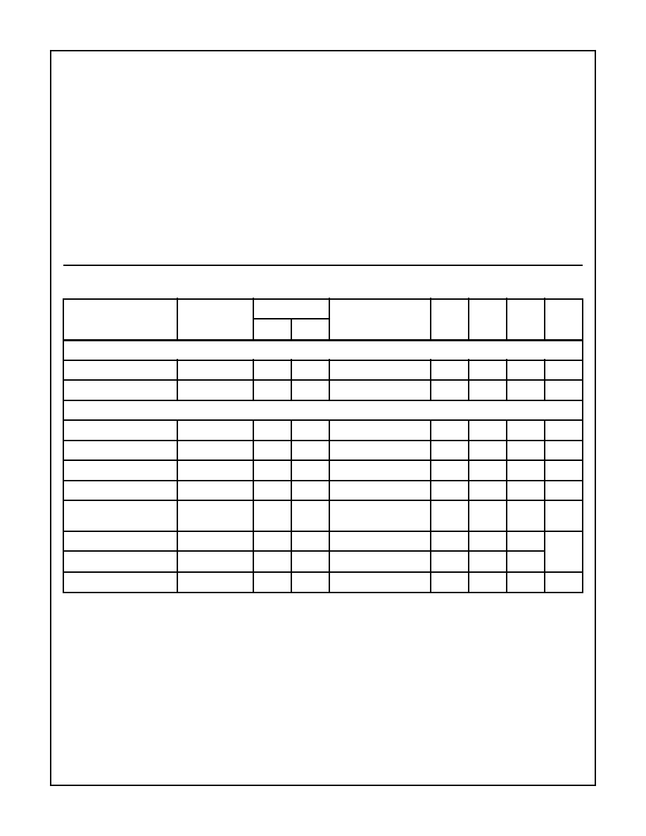
Electrical Specifications
T
A
= 25
o
C, Chroma Gain Control at maximum position for all tests except as noted. Electrical
specifications referenced to test circuit.
PARAMETER
TERMINAL,
MEASUREMENT
AND SYMBOL
SWITCH POS.
V
CHROMA
INPUT TP
1
UNITS
S
1
S
2
MIN
TYP
MAX
DC ELECTRICAL SPECIFICATIONS
Voltage Regulator
V
12
2
2
0
10.1
11.2
12.1
V
Supply Current
I
12
2
2
0
16
25
38
mA
SWITCHING ELECTRICAL SPECIFICATIONS (Note 3)
Pull-In Range (Note 4)
V
8
(Note 6)
2
0.5V
P-P
±
250
-
-
Hz
Oscillator Output
V
8
2
2
0
0.6
1.0
-
V
P-P
100% Chroma Output
V
15
1
2
0.5V
P-P
1.4
2.7
-
V
P-P
Overload Detector
V
15
1
1
0.5V
P-P
0.4
-
0.7
V
P-P
Minimum Chroma Output
(Note 5)
V
15
1
2
0.5V
P-P
-
-
20
mV
P-P
200% Chroma Output
V
15
1
2
1V
P-P
70
100
140
% of
100%
Reading
20% Chroma Output
V
15
1
2
0.1V
P-P
40
-
105
Kill Level
V
TP1
1
2
Vary
5
-
60
mV
P-P
NOTES:
3. Except for pull-in range testing, tune oscillator trimmer capacitor for free running frequency of 3.579545MHz
±
10Hz.
4. Set Switch 1 to Position 2, detune oscillator
±
250Hz, set Switch 1 to Position 1, and check for oscillator pull-in.
5. Set Chroma Gain Control to minimum position (CCW).
CA3126