 | –≠–ª–µ–∫—Ç—Ä–æ–Ω–Ω—ã–π –∫–æ–º–ø–æ–Ω–µ–Ω—Ç: CA3141 | –°–∫–∞—á–∞—Ç—å:  PDF PDF  ZIP ZIP |

1
Semiconductor
January 1999
CA3141
High-Voltage Diode Array For Commercial,
Industrial and Military Applications
Features
∑ Matched Monolithic Construction
- V
F
Match (Each Diode Pair) . . . . 0.55mV At I
F
= 1mA
∑ Low Diode Capacitance. . . . . . . 0.3pF (Typ) at V
R
= 2V
∑ High Diode-to-Substrate Breakdown. . . . . . . . . 30V (Min)
∑ Low Reverse (Leakage) Current . . . . . . . 100nA (Max)
Applications
∑ Balanced Modulators or Demodulators
∑ Analog Switches
∑ High-Voltage Diode Gates
∑ Current Ratio Detectors
Description
The CA3141E High Voltage Diode Array Consists of ten gen-
eral purpose high reverse breakdown diodes. Six diodes are
internally connected to form three common cathode diode
pairs, and the remaining four diodes are internally connected
to form two common anode diode pairs. Integrated circuit
construction assures excellent static and dynamic matching
of the diodes, making the CA3141 extremely useful for a
wide variety of applications in communications and switching
systems.
Pinout
CA3141
(PDIP)
TOP VIEW
Part Number Information
PART NUMBER
TEMP.
RANGE (
o
C)
PACKAGE
PKG.
NO.
CA3141E
-55 to 125
16 Ld PDIP
E16.3
14
15
16
9
13
12
11
10
1
2
3
4
5
7
6
8
D
1
D
2
D
10
D
9
D
3
D
4
D
7
D
8
D
5
D
6
CAUTION: These devices are sensitive to electrostatic discharge. Users should follow proper IC Handling Procedures.
Copyright
©
Harris Corporation 1999
File Number
906.4
OBSOLETE PR
ODUCT
NO RECOMMENDED REPLA
CEMENT
Call Central Applications 1-800-442-7747
or email: centapp@harris.com

2
Absolute Maximum Ratings
Thermal Information
Inverse Voltage (PIV) . . . . . . . . . . . . . . . . . . . . . . . . . . . . . . . . . 30V
Peak Diode -to-Substrate Voltage . . . . . . . . . . . . . . . . . . . . . . . 30V
Peak Forward Surge Current [I
F
(Surge)] . . . . . . . . . . . . . . . . 100mA
DC Forward Current (I
F
) . . . . . . . . . . . . . . . . . . . . . . . . . . . . . . 25mA
Operating Conditions
Temperature Range . . . . . . . . . . . . . . . . . . . . . . . . . -55
o
C to 125
o
C
Thermal Resistance (Typical, Note 1)
JA
(
o
C/W)
PDIP Package . . . . . . . . . . . . . . . . . . . . . . . . . . . . .
90
Maximum Power Dissipation (Any One Diode) . . . . . . . . . . . . . . 50mW
Maximum Junction Temperature (Die). . . . . . . . . . . . . . . . . . . . 175
o
C
Maximum Junction Temperature (Plastic Package) . . . . . . . . 150
o
C
Maximum Storage Temperature Range . . . . . . . . . .-65
o
C to 150
o
C
Maximum Lead Temperature (Soldering 10s) . . . . . . . . . . . . . 300
o
C
CAUTION: Stresses above those listed in "Absolute Maximum Ratings" may cause permanent damage to the device. This is a stress only rating and operation
of the device at these or any other conditions above those indicated in the operational sections of this specification is not implied.
NOTE:
1.
JA
is measured with the component mounted on an evaluation PC board in free air.
Electrical Specifications
T
A
= 25
o
C
PARAMETER
SYMBOL
TEST CONDITIONS
MIN
TYP
MAX
UNITS
DC Forward Voltage Drop
V
F
I
F
(Anode)
100
µ
A
-
0.7
0.9
V
1mA
-
0.78
1
V
10mA
-
0.93
1.2
V
DC Reverse Breakdown Voltage
V
(BR)R
I
F
= -10
µ
A
30
50
-
V
DC Breakdown Voltage Between Any Diode and
Substrate
V
(BR)DI
I
DI
= 10
µ
A
30
50
-
V
DC Reverse (Leakage) Current
I
R
V
F
= -20V
-
-
100
nA
DC Reverse (Leakage) Current Between Any Diode
and Substrate
I
DI
V
DI
= 20V
-
-
100
nA
Magnitude of Diode Offset Voltage Between Diode Pairs
V
DI
= 20V, I
FA
= 1mA
-
0.55
-
mV
Temperature Coefficient of Forward Voltage Drop
V
F
/
T
I
F
= 1mA
-
-1.5
-
mV/
o
C
Reverse Recovery Time
tRR
I
F
= 2mA, I
R
= 2mA
-
50
-
ns
Diode Capacitance
C
D
See Figure 4
pF
Diode Anode-to-Substrate Capacitance
C
DAI
See Figure 5
pF
Diode Cathode-to-Substrate Capacitance
C
DCI
See Figure 6
pF
Magnitude of Cathode-to-Anode Current Ratio
|I
FC
/I
FA
|
I
FA
= 1mA, V
DS
= 10V
0.9
0.96
-
-
Typical Performance Curves
FIGURE 1. DC FORWARD VOLTAGE DROP vs FORWARD
CURRENT
FIGURE 2. DC FORWARD VOLTAGE DROP vs
TEMPERATURE
FORWARD CURRENT (
µ
A)
DC FOR
W
ARD V
O
L
T
A
GE DR
OP (V)
T
A
= 25
o
C
1
0.8
0.6
0.4
0.2
0
0.1
1
10
10
2
10
3
10
4
DC FOR
W
ARD V
O
L
T
A
GE DR
OP (V)
1.2
0.8
0.6
0.4
0.2
0
-100
1
-50
0
50
100
150
TEMPERATURE (
o
C)
I
F
= 10mA
I
F
= 3mA
I
F
= 1mA
I
F
= 300
µ
A
I
F
= 100
µ
A
I
F
= 10
µ
A
I
F
= 1
µ
A
I
F
= 100nA
CA3141

3
FIGURE 3. 3. DIODE OFFSET VOLTAGE vs MAGNITUDE OF
ANODE CURRENT
FIGURE 4. DIODE CAPACITANCE vs CATHODE-TO-ANODE
REVERSE VOLTAGE
FIGURE 5. DIODE ANODE-TO-SUBSTRATE CAPACITANCE vs
REVERSE VOLTAGE
FIGURE 6. DIODE CATHODE-TO-SUBSTRATE CAPACITANCE vs
CATHODE-TO-SUBSTRATE DC REVERSE VOLTAGE
FIGURE 7. FORWARD (CATHODE) CURRENT vs FORWARD
(ANODE) CURRENT
FIGURE 8. DC LEAKAGE CURRENT vs TEMPERATURE
Typical Performance Curves
(Continued)
MAGNITUDE OF ANODE CURRENT (
µ
A)
DIODE OFFSET V
O
L
T
A
GE (mV)
0
1
10
10
2
10
3
10
4
10
5
0.5
1
1.5
2
2.5
3
T
A
= 25
o
C
|V
F1
- V
F2
| , |V
F3
- V
F4
| , |V
F5
- V
F6
|
|V
F7
- V
F8
| , |V
F9
- V
F10
|
CATHODE-TO-ANODE DC REVERSE VOLTAGE (V)
DIODE CAP
A
CIT
ANCE (pF)
0
0
0.2
0.4
0.6
0.8
1
1.2
5
10
15
20
T
A
= 25
o
C
D
5
, D
9
D
7
, D
8
D
1
, D
6
D
3
, D
10
D
2
D
4
T
A
= 25
o
C
ANODE (TERMINALS 2, 8, 11, 16)
ANODE (TERMINAL 1)
ANODE (TERMINAL 15)
ANODE (TERMINALS 4, 5)
DIODE ANODE-T
O-SUBSTRA
TE
CAP
A
CIT
ANCE (pF)
1.6
1.5
1.4
1.3
1.2
1.1
1
0.9
0.8
0.7
0.6
0.5
ANODE-TO-SUBSTRATE DC REVERSE VOLTAGE (V)
0
1
2
3
4
5
6
7
8
9
10
T
A
= 25
o
C
CATHODE (TERMINALS 3, 6, 14)
DIODE CA
THODE-T
O-SUBSTRA
TE
CAP
A
CIT
ANCE (pF)
CATHODE-TO-SUBSTRATE DC REVERSE VOLTAGE (V)
CATHODE (TERMINALS 7, 10, 12, 13)
12
10
8
6
4
2
0
0
5
10
15
20
T
A
= 25
o
C
V
DI
= 10V
FOR
W
ARD (CA
THODE) CURRENT (mA)
FORWARD (ANODE) CURRENT (mA)
10
1
0.1
0.01
0.01
0.1
1
10
DC LEAKA
GE CURRENT (pA)
TEMPERATURE (
o
C)
DIODE-TO-SUBSTRATE
LEAKAGE CURRENT
DIODE REVERSE
(LEAKAGE) CURRENT
10
5
10
4
10
3
10
2
10
1
0.1
-100
-50
0
50
100
150
CA3141
4
CA3141
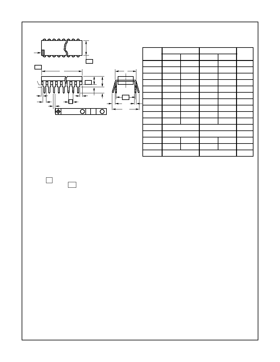
NOTES:
1. Controlling Dimensions: INCH. In case of conflict between
English and Metric dimensions, the inch dimensions control.
2. Dimensioning and tolerancing per ANSI Y14.5M-1982.
3. Symbols are defined in the "MO Series Symbol List" in Section
2.2 of Publication No. 95.
4. Dimensions A, A1 and L are measured with the package seated
in JEDEC seating plane gauge GS-3.
5. D, D1, and E1 dimensions do not include mold flash or protru-
sions. Mold flash or protrusions shall not exceed 0.010 inch
(0.25mm).
6. E and
are measured with the leads constrained to be per-
pendicular to datum
.
7. e
B
and e
C
are measured at the lead tips with the leads uncon-
strained. e
C
must be zero or greater.
8. B1 maximum dimensions do not include dambar protrusions.
Dambar protrusions shall not exceed 0.010 inch (0.25mm).
9. N is the maximum number of terminal positions.
10. Corner leads (1, N, N/2 and N/2 + 1) for E8.3, E16.3, E18.3,
E28.3, E42.6 will have a B1 dimension of 0.030 - 0.045 inch
(0.76 - 1.14mm).
C
L
E
e
A
C
e
B
e
C
-B-
E1
INDEX
1 2 3
N/2
N
AREA
SEATING
BASE
PLANE
PLANE
-C-
D1
B1
B
e
D
D1
A
A2
L
A1
-A-
0.010 (0.25)
C
A
M
B S
e
A
-C-
Dual-In-Line Plastic Packages (PDIP)
E16.3
(JEDEC MS-001-BB ISSUE D)
16 LEAD DUAL-IN-LINE PLASTIC PACKAGE
SYMBOL
INCHES
MILLIMETERS
NOTES
MIN
MAX
MIN
MAX
A
-
0.210
-
5.33
4
A1
0.015
-
0.39
-
4
A2
0.115
0.195
2.93
4.95
-
B
0.014
0.022
0.356
0.558
-
B1
0.045
0.070
1.15
1.77
8, 10
C
0.008
0.014
0.204
0.355
-
D
0.735
0.775
18.66
19.68
5
D1
0.005
-
0.13
-
5
E
0.300
0.325
7.62
8.25
6
E1
0.240
0.280
6.10
7.11
5
e
0.100 BSC
2.54 BSC
-
e
A
0.300 BSC
7.62 BSC
6
e
B
-
0.430
-
10.92
7
L
0.115
0.150
2.93
3.81
4
N
16
16
9
Rev. 0 12/93