 | –≠–ª–µ–∫—Ç—Ä–æ–Ω–Ω—ã–π –∫–æ–º–ø–æ–Ω–µ–Ω—Ç: CD22100E | –°–∫–∞—á–∞—Ç—å:  PDF PDF  ZIP ZIP |
4-184
Semiconductor
Description
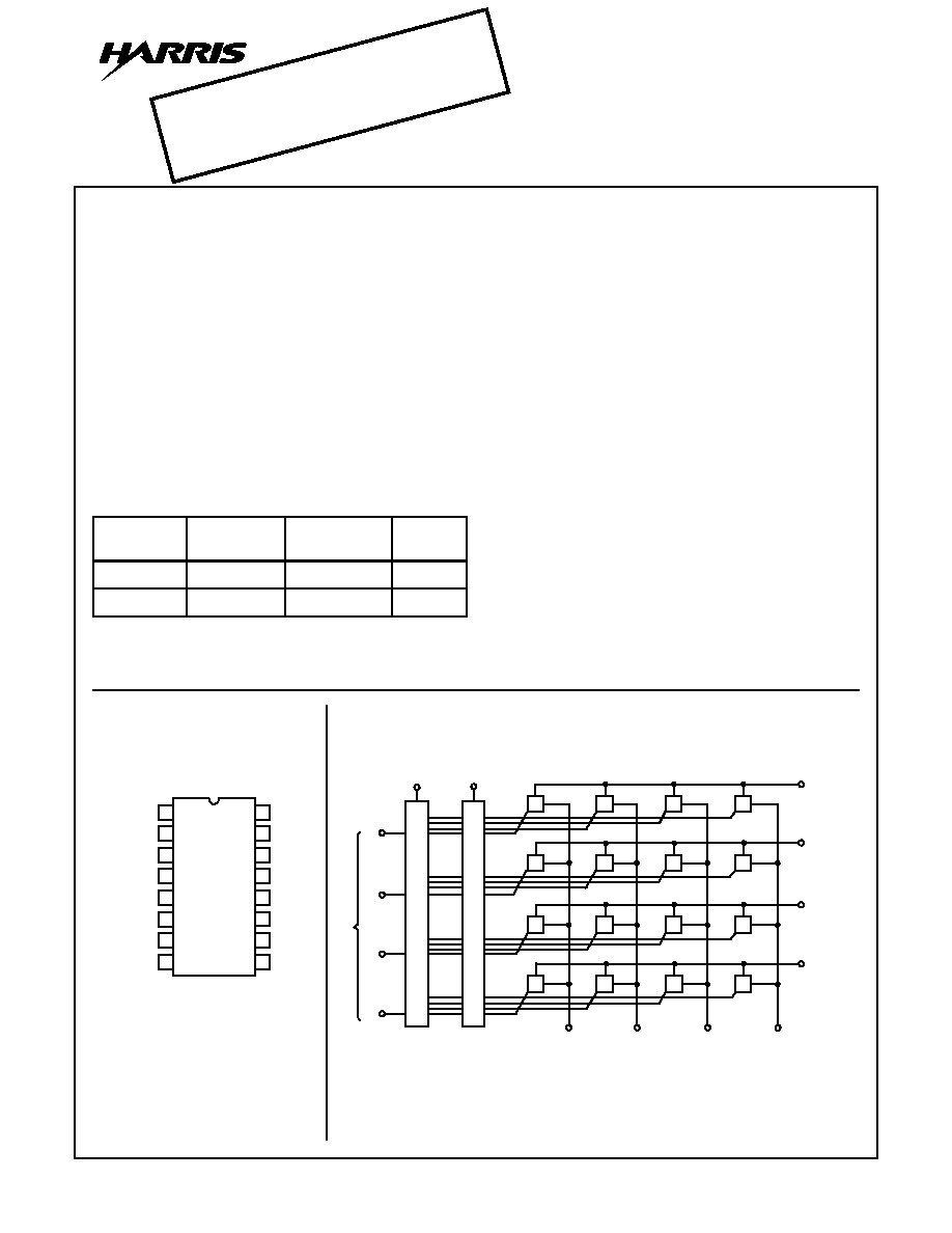
CD22100 combines a 4 x 4 array of crosspoints (transmis-
sion gates) with a 4-line to 16-line decoder and 16 latch
circuits. Any one of the sixteen transmission gates (cross-
points) can be selected by applying the appropriate four line
address. The selected transmission gate can be turned on or
off by applying a logic one or zero, respectively, to the data
input and strobing the strobe input to a logic one. Any
number of the transmission gates can be ON simultaneously.
When the required operating power is applied to the
CD22100, the states of the 16 switches are indeterminate.
Therefore, all switches must be turned off by putting the
strobe high and data in low, and then addressing all switches
in succession.
Features
∑ Low ON Resistance . . . . . . . . . .75
(Typ) at V
DD
= 12V
∑ "Built-In" Control Latches
∑ Large Analog Signal Capability
. . . . . . . . . . . . . . . ±
V
DD
/2
∑ 10MHz Switch Bandwidth
∑ Matched Switch Characteristics
R
ON
= 18
(Typ) at
V
DD
= 12V
∑ High Linearity - 0.5% Distortion (Typ) at f = 1kHz,
V
IN
= 5V
P-P
, V
DD
= 10V, and R
L
= 1k
∑ Standard CMOS Noise Immunity
∑ 100% Tested for Maximum Quiescent Current at 20V
Ordering Information
PART
NUMBER
TEMP. RANGE
(
o
C)
PACKAGE
PKG. NO.
CD22100E
-40 to 85
16 Ld PDIP
E16.3
CD22100F
-55 to 125
16 Ld CERDIP
F16.3
February 1999
Pinout
CD22100
(PDIP, CERDIP)
TOP VIEW
Functional Diagram
14
15
16
9
13
12
11
10
1
2
3
4
5
7
6
8
V
DD
V
SS
Y1
Y2
X4
X3
Y4
Y3
X1
STROBE
X2
DATA IN
C
D
B
A
ADDRESS
4-LINE T
O
16-LINE DECODER
16 CONTR
OL LA
TCHES
12
13
14
15
0
1
2
3
4
5
6
7
8
9
10
11
DATA
IN
2
STROBE
7
6
A
5
B
3
C
4
D
X1
X2
X3
X4
9
1
12
13
Y4
11
Y3
10
Y2
14
Y1
15
CAUTION: These devices are sensitive to electrostatic discharge. Users should follow proper IC Handling Procedures.
Copyright
©
Harris Corporation 1999
File Number
1076.4
CD22100
CMOS 4 x 4 Crosspoint Switch with Control Memory
High-Voltage Type (20V Rating)
[ /Title
(CD22
100)
/Sub-
ject
(CMO
S 4 x 4
Cross-
point
Switch
with
Con-
trol
Mem-
ory
High-
Volt-
age
Type
(20V
Rat-
ing))
/
Author
()
/Key-
words
(Har-
ris
Semi-
con-
ductor,
Tele-
com,
SLICs,
SLACs
, Tele-
phone,
OBSOLETE PR
ODUCT
NO RECOMMENDED REPLA
CEMENT
Call Central Applications 1-800-442-7747
or email: centapp@harris.com
4-185
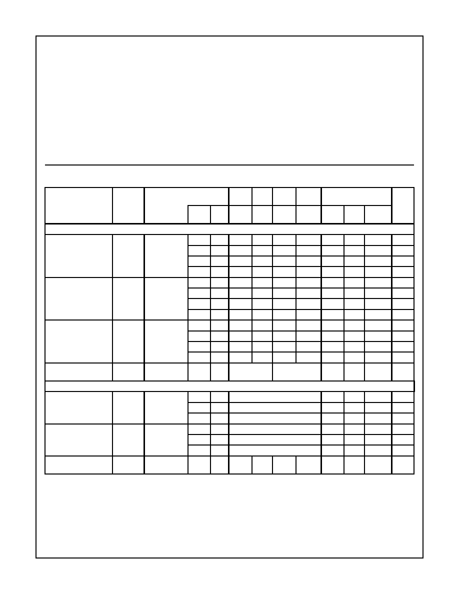
CD22100
Absolute Maximum Ratings
Thermal Information
Supply Voltage (Referenced to VSS Terminal) . . . . . . . . .-0.5 to 20V
Input Voltage (All Inputs) . . . . . . . . . . . . . . . . . . . . -0.5 to V
DD
0.5V
Input Current (Any one input (Note 1))
. . . . . . . . . . . . . . . . . . . .±
10mA
Power Dissipation
For T
A
= -40
o
C to 60
o
C (Package Type E) . . . . . . . . . . . . 500mW
For T
A
= 60
o
C to 85
o
C
(Package Type E) . . . . . . . . Derate Linearly 12mW/
o
C to 200mW
For T
A
= -55
o
C to 100
o
C (Package Type F) . . . . . . . . . . . 500mW
For T
A
= 100
o
C to 125
o
C
(Package Type F) . . . . . . . . Derate Linearly 12mW/
o
C to 200mW
Device Dissipation per Transmission Gate
For T
A
= Full Package Temperature Range (All Types) . . . . . 100mW
Maximum Junction Temperature . . . . . . . . . . . . . . . . . . . . . . . 175
o
C
Maximum Junction Temperature (Plastic Package) . . . . . . . . 150
o
C
Storage Temperature Range . . . . . . . . . . . . . . . -65
o
C
T
A
150
o
C
Maximum Lead Temperature (Soldering 10s) . . . . . . . . . . . . . 300
o
C
Operating Conditions
Temperature Range
Package Type F . . . . . . . . . . . . . . . . . . . . . . . -55
o
C
T
A
125
o
C
Package Type E . . . . . . . . . . . . . . . . . . . . . . . . -40
o
C
T
A
85
o
C
Supply Voltage Range
For T
A
= Full Package Temperature Range . . . . . . . . . . . . . . 3V to 18V
CAUTION: Stresses above those listed in "Absolute Maximum Ratings" may cause permanent damage to the device. This is a stress only rating and operation
of the device at these or any other conditions above those indicated in the operational sections of this specification is not implied.
Electrical Specifications
Values at -55
o
C, 25
o
C, 125
o
C Apply to F Package
Values at -40
o
C, 25
o
C, 85
o
C Apply to E Package
PARAMETER
SYMBOL
TEST
CONDITIONS
-55
o
C
-40
o
C
85
o
C
125
o
C
25
o
C
UNITS
FIG.
V
DD
(V)
MAX
MAX
MAX
MAX
MIN
TYP
MAX
STATIC CROSSPOINTS
Quiescent Device
Current
I
DD
(Max)
1
5
5
5
150
150
-
0.04
5
µ
A
1
10
10
10
300
300
-
0.04
10
µ
A
1
15
20
20
600
600
-
0.04
20
µ
A
1
20
100
100
3000
3000
-
0.08
100
µ
A
On Resistance
R
ON
(Max) Any Switch
V
IS
= 0 to V
DD
11
5
475
500
725
800
-
225
600
12
10
135
145
205
230
-
85
180
-
12
100
110
155
175
-
75
135
13
15
70
75
110
125
-
65
95
R
ON
Resistance
R
ON
Between any
two switches
-
5
-
-
-
-
-
25
-
-
10
-
-
-
-
-
10
-
-
12
-
-
-
-
-
8
-
-
15
-
-
-
-
-
5
-
OFF Switch Leakage
Current
I
L
(Max)
All switches
OFF, V
IS
= 18V
3
18
±
100
±
1000
-
±
1
±
100
(Note 2)
nA
STATIC CONTROLS
Input Low Voltage
V
IL
(Max) OFF switch
I
L
< 0.2
µ
A
-
5
1.5
-
-
1.5
V
-
10
3
-
-
3
V
-
15
4
-
-
4
V
Input High Voltage
V
IH
(Min)
ON switch
see R
ON
characteristic
-
5
3.5
3.5
-
-
V
-
10
7
7
-
-
V
-
15
11
11
-
-
V
Input Current
I
IN
(Max)
Any control
V
IN
= 0, 18V
2
18
±
0.1
±
0.1
±
1
±
1
-
±
10
-5
±
0.1
µ
A
NOTES:
1. Maximum current through transmission gates (switches) = 25mA.
2. Determined by minimum feasible leakage measurement for automatic testing.
4-186
CD22100
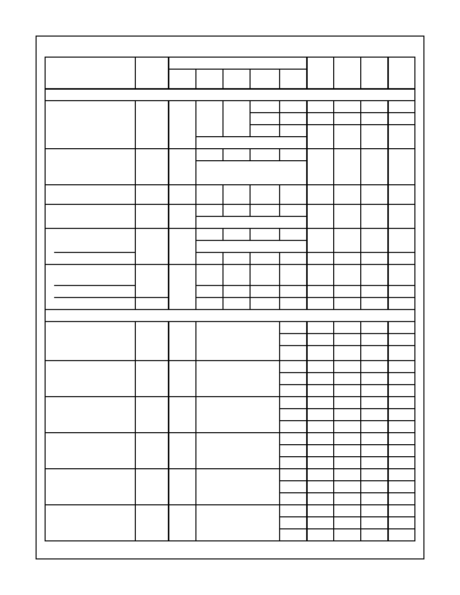
Electrical Specifications
T
A
= 25
o
C
PARAMETER
SYMBOL
TEST CONDITIONS
MIN
TYP
MAX
UNITS
FIGURE
f
IS
(kHz)
R
L
(k
)
V
IS
(V)
(Note 3)
V
DD
(V)
DYNAMIC CROSSPOINTS
Propagation Delay Time,
(Switch ON) Signal Input to
Output
t
PHL
, t
PLH
5
-
10
5
5
-
30
60
ns
10
10
-
15
30
ns
15
15
-
10
20
ns
C
L
= 50pF; t
R
, t
F
= 20ns
Frequency Response (Any
Switch ON)
f
3dB
16
1
1
5
10
-
40
-
MHz
Sine Wave Input,
Sine Wave Response
(Distortion)
THD
1
1
5
10
-
0.5
-
%
Feedthrough (All switches OFF)
F
DT
1.6
1
5
10
-
-80
-
dB
Sine Wave Input
Frequency for Signal Crosstalk
F
CT
7
-
1
10
10
Attenuation of 40dB
Sine Wave Input
-
1.5
-
MHz
Attenuation of 110dB
-
-
-
-
-
0.1
-
kHz
Capacitance:
C
IS
Xn to Ground
-
-
-
5 - 15
-
18
-
pF
Yn to Ground
-
-
-
5 - 15
-
30
-
pF
Feedthrough
C
IOS
-
-
-
-
-
0.4
-
pF
DYNAMIC CONTROLS
Propagation Delay Time:
t
PZH
8
R
L
= 1k
,
C
L
= 50pF,
t
R
, t
F
= 20ns
5
-
300
600
ns
Strobe to Output
(Switch Turn-ON to High
Level)
10
-
125
250
ns
15
-
80
160
ns
Propagation Delay Time:
t
PZH
9
R
L
= 1k
,
C
L
= 50pF,
t
R
, t
F
= 20ns
5
-
110
220
ns
Data-In to Output
(Turn-ON to High Level)
10
-
40
80
ns
15
-
25
50
ns
Propagation Delay Time:
t
PZH
10
R
L
= 1k
,
C
L
= 50pF,
t
R
, t
F
= 20ns
5
-
350
700
ns
Address to Output
(Turn-ON to High Level)
10
-
135
270
ns
15
-
90
180
ns
Propagation Delay Time:
t
PHZ
8
R
L
= 1k
,
C
L
= 50pF,
t
R
, t
F
= 20ns
5
-
165
330
ns
Strobe to Output
(Switch Turn-OFF)
10
-
85
170
ns
15
-
70
140
ns
Propagation Delay Time:
t
PZL
9
R
L
= 1k
,
C
L
= 50pF,
t
R
, t
F
= 20ns
5
-
210
420
ns
Data-In to Output
(Turn-ON to Low Level)
10
-
110
220
ns
15
-
100
200
ns
Propagation Delay Time:
t
PHZ
10
R
L
= 1k
,
C
L
= 50pF,
t
R
, t
F
= 20ns
5
-
435
870
ns
Address to Output
(Turn-OFF)
10
-
210
420
ns
15
-
160
320
ns
20 log
V
OS
V
IS
------------
-3dB
=
4-187
CD22100
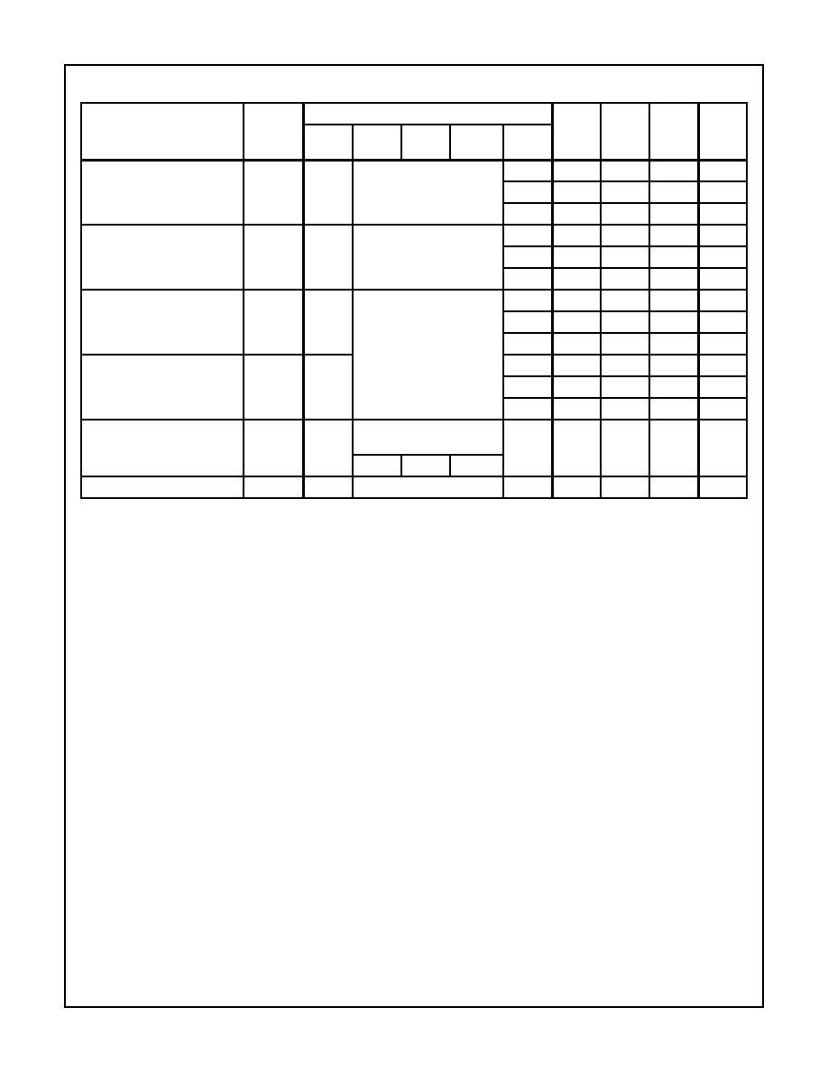
Minimum Setup Time
Data-In to Strobe, Address
t
S
8, 10
R
L
= 1k
,
C
L
= 50pF,
t
R
, t
F
= 20ns
5
-
95
190
ns
10
-
25
50
ns
15
-
15
30
ns
Minimum Hold Time
Data-In to Strobe, Address
t
H
8, 10
R
L
= 1k
,
C
L
= 50pF,
t
R
, t
F
= 20ns
5
-
180
360
ns
10
-
110
220
ns
15
-
35
70
ns
Maximum Switching Frequency
f
ÿ
R
L
= 1k
,
C
L
= 50pF,
t
R
, t
F
= 20ns
5
0.6
1.2
-
MHz
10
1.6
3.2
-
MHz
15
2.5
5
-
MHz
Minimum Strobe Pulse Width
t
W
8
5
-
300
600
ns
10
-
120
240
ns
15
-
90
180
ns
Control Crosstalk, Data-In,
Address or Strobe to Output
6
Square Wave Input;
t
R
, t
F
= 20ns
10
-
75
-
mV
PEAK
-
10
10
Input Capacitance
C
IN
Any Control Input
-
-
5
7.5
pF
NOTE:
3. Peak-to-peak voltage symmetrical about
.
Electrical Specifications
T
A
= 25
o
C (Continued)
PARAMETER
SYMBOL
TEST CONDITIONS
MIN
TYP
MAX
UNITS
FIGURE
f
IS
(kHz)
R
L
(k
)
V
IS
(V)
(Note 3)
V
DD
(V)
V
DD
2
-------------
4-188
CD22100
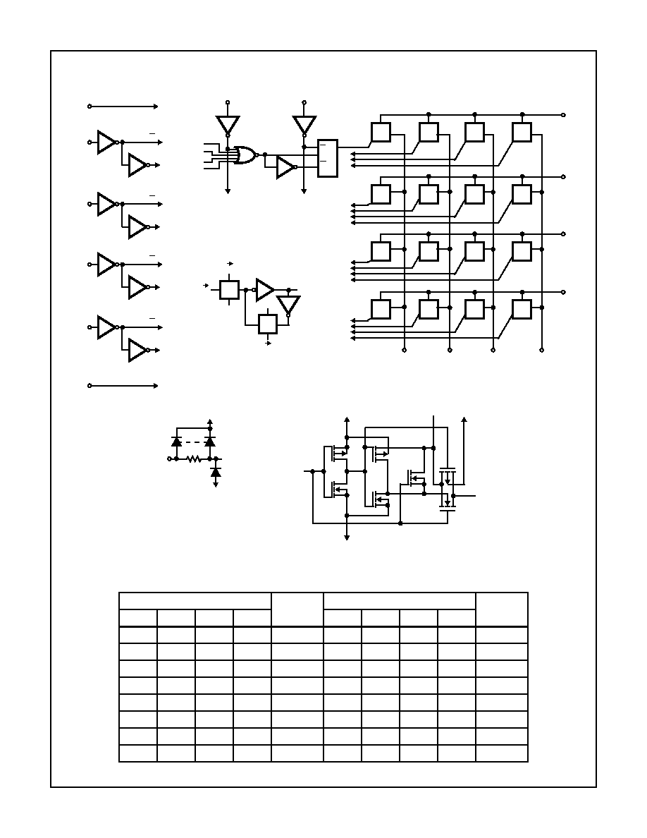
Schematic Diagram
TRUTH TABLE
ADDRESS
SELECT
ADDRESS
SELECT
A
B
C
D
A
B
C
D
0
0
0
0
X1Y1
0
0
0
1
X1Y3
1
0
0
0
X2Y1
1
0
0
1
X2Y3
0
1
0
0
X3Y1
0
1
0
1
X3Y3
1
1
0
0
X4Y1
1
1
0
1
X4Y3
0
0
1
0
X1Y2
0
0
1
1
X1Y4
1
0
1
0
X2Y2
1
0
1
1
X2Y4
0
1
1
0
X3Y2
0
1
1
1
X3Y4
1
1
1
0
X4Y2
1
1
1
1
X4Y4
(NOTE)
6
A
A
A
(NOTE)
5
B
B
B
(NOTE)
3
C
C
C
(NOTE)
4
D
D
D
V
SS
8
V
DD
16
A
B
C
D
D Q
¯
¯
0
1
2
3
LATCH
¯
= 1
ENABLES DATA
TG
TG
TG
TG
4
5
6
7
TG
TG
TG
TG
8
9
10
11
TG
TG
TG
TG
12
13
14
15
TG
TG
TG
TG
9
1
12
13
11
10
14
15
Y4
Y3
Y2
Y1
X4
X3
X2
X1
D
Q
¯
¯
p
n
¯
¯
p
n
DETAIL OF LATCHES
TO OTHER DECODER
GATES/LATCHES
V
DD
V
DD
V
SS
IN
OUT
Q
DETAIL OF TRANSMISSION GATES
(NOTE)
STROBE
7
2
(NOTE)
DATA IN
V
DD
V
SS
NOTE: INPUTS PROTECTED
BY COS/MOS
PROTECTION
NETWORK
(1 OF 16)
LEVEL TRIGGERED