4-165
Semiconductor
February 1999
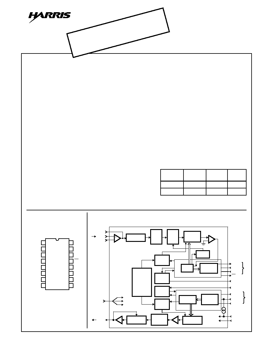
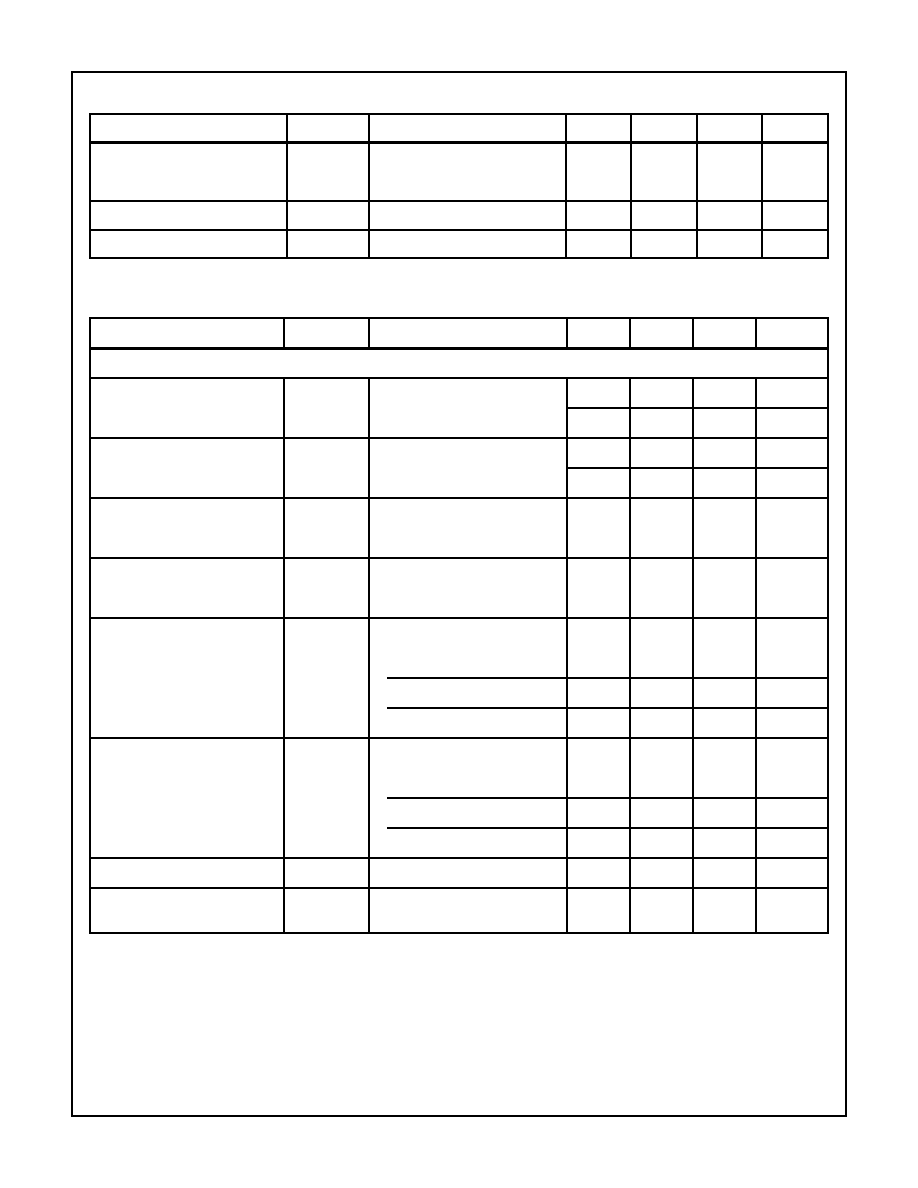
Pinout
CD22354A, CD22357A
(PDIP)
TOP VIEW
Functional Block Diagram
FULL-FEATURE PCM CODEC
14
15
16
9
13
12
11
10
1
2
3
4
5
7
6
8
BCLK
X
MCLK
X
D
X
FS
X
GS
X
VF
X
1+
VF
X
1-
TS
X
V-
GND
VF
R
O
V+
FS
R
D
R
BCLK
R
/
CLKSEL
MCLK
R
/
PDN
R
CV
V
REF
XMIT
V
REF
COMPARATOR
XMIT
CLOCK
CIRCUIT
BAND
GAP
REFERENCE
XMIT DIGITAL
R
CV
DIGITAL
3
VF
R
O
+5V
-5V
V+
V-
11
10
12
13
9
8
5
7
6
4
D
X
FS
X
FS
R
D
R
PARALLEL
TO
SERIAL
S.A.R.
SIGN
BIT INT.
TRANSMIT
D/A
LADDER
RECEIVE
FILTER
FILTER
RECEIVE
D/A LADDER
FILTER
XMIT
LOW
PASS
FILTER
XMIT
HIGH
PASS
FILTER
14
+
15
2
BCLK
R
/
CLKSEL
MCLK
R
/
PDN
MCLK
X
SERIAL
TO
PARALLEL
D/A
REGISTER
BCLK
X
TS
X
16
1
SMOOTHING
GND
VF
X
1+
VF
X
1-
GS
X
ANTI-ALLAS
LOW PASS
R
CV
CLOCK
CIRCUIT
FR
OM SLIC
T
O
SLIC
DDIGIT
AL OUT
DDIGIT
AL IN
CD22354A,
CD22357A
CMOS Single-Chip,
Full-Feature PCM CODEC
File Number
1682.4
CAUTION: These devices are sensitive to electrostatic discharge. Users should follow proper IC Handling Procedures.
Copyright
�
Harris Corporation 1999
Description
The CD22354A and CD22357A are monolithic silicon-
gate, double-poly CMOS integrated circuits containing
the band-limiting filters and the companding A/D and D/A
conversion circuits that conform to the AT&T D3/D4
specifications
and
CCITT
recommendations.
The
CD22354A provides the AT&T
�
-law and the CD22357A
provides the CCITT A-law companding characteristic.
The primary applications for the CD22354A and
CD22357A are in telephone systems. These circuits
perform the analog and digital conversions between the
subscriber loop and the PCM highway in a digital
switching system. The functional block diagram is
shown below.
With flexible features, including synchronous and
asynchronous operations and variable data rates, the
CD22354A and CD22357A are ideally suited for PABX,
central office switching system, digital telephones as
well as other applications that require accurate A/D and
D/A conversions and minimal conversion time.
Ordering Information
PART
NUMBER
TEMP.
RANGE (
o
C)
PACKAGE PKG. NO.
CD22354AE
-40 to 80
16 Ld PDIP E16.3
CD22357AE
-40 to 80
16 Ld PDIP E16.3
Features
� Meets or Exceeds All AT&T D3/D4 Specifications and CCITT
Recommendations
� Complete CODEC and Filtering Systems: No External Components
for Sample-and-Hold and Auto-Zero Functions. Receive Output Fil-
ter with (SIN X)/X Correction and Additional 8kHz Suppression
� Variable Data Clocks - From 64kHz . . . . . . . . . . . . . . . . . . . . . 2.1MHz
� Receiver Includes Power-Up Click Filter
� TTL or CMOS-Compatible Logic
� ESD Protection on All Inputs and Outputs
Applications
� PABX
� Central Office Switching Systems
� Accurate A/D and D/A Conversions
� Digital Telephones
� Cellular Telephone Switching Systems
� Voice Scramblers - Descramblers
� T1 Conference Bridges
� Voice Storage and Retrieval Systems
� Sound Based Security Systems
� Computerized Voice Analysis
� Mobile Radio Telephone Systems
� Microwave Telephone Networks
� Fiber-Optic Telephone Networks
[ /Title
(CD22
354A,
CD223
57A)
/Sub-
ject
(CMO
S Sin-
gle-
Chip,
Full-
Fea-
ture
PCM
CODE
C)
/
Author
()
/Key-
words
(Har-
ris
Semi-
con-
ductor,
RSLIC
18,
Tele-
com,
SLICs,
SLACs
, Tele-
phone,
Tele-
phony,
WLL,
Wire-
less
Local
Loop,
OBSOLETE PR
ODUCT
NO RECOMMENDED REPLA
CEMENT
Call Central Applications 1-800-442-7747
or email: centapp@harris.com
4-166
CD22354A, CD22357A
Absolute Maximum Ratings
Thermal Information
DC Supply-Voltage, (V+) . . . . . . . . . . . . . . . . . . . . . . . . . .-0.5 to 7V
DC Supply-Voltage, (V-) . . . . . . . . . . . . . . . . . . . . . . . . . . .0.5 to -7V
DC Input Diode Current,
I
IK
(V
I
< V- -0.5V or V
I
> V+ 0.5V)
. . . . . . . . . . . . . . . . . . . . . . . .�
20mA
DC Output Diode Current,
I
OK
(V
I
< V- -0.5V or V
O
> V+ 0.5V)
. . . . . . . . . . . . . . . . . . . . . . .�
20mA
DC Drain Current, Per Output
I
O
(V- -0.5V < V
O
< V+ 0.5V)
. . . . . . . . . . . . . . . . . . . . . . . . . . . .�
25mA
DC Supply/Ground Current
. . . . . . . . . . . . . . . . . . . . . . . . . . . . .�
50mA
Power Dissipation Per Package (P
D
):
For T
A
= -40
o
C to 60
o
C . . . . . . . . . . . . . . . . . . . . . . . . . . . 500mW
For T
A
= 60
o
C to 85
o
C . . . . . . . . . . . . Derate Linearly at 8mW/
o
C
to 300mW
Maximum Junction Temperature . . . . . . . . . . . . . . . . . . . . . . . 175
o
C
Maximum Junction Temperature (Plastic Package) . . . . . . . . 150
o
C
Maximum Storage Temperature Range (T
STG
) . . . . . -65
o
C to 150
o
C
Maximum Lead Temperature (Soldering 10s) . . . . . . . . . . . . . 300
o
C
Operating Conditions
Operating-Temperature Range (T
A
) . . . . . . . . . . . . . . -40
o
C to 80
o
C
CAUTION: Stresses above those listed in "Absolute Maximum Ratings" may cause permanent damage to the device. This is a stress only rating and operation
of the device at these or any other conditions above those indicated in the operational sections of this specification is not implied.
Electrical Specifications
At T
A
= 25
o
C
PARAMETER
SYMBOL
TEST CONDITIONS
MIN
TYP
MAX
UNITS
STATIC SPECIFICATIONS
Positive Power Supply
V+
4.75
5
5.25
V
Negative Power Supply
V-
-4.75
-5
-5.25
V
Power Dissipation (Operating)
P
OPR
V+ = 5V
-
75
90
mW
Power Dissipation (Standby)
P
STBY
V- = -5V
-
9
15
mW
Electrical Specifications
At T
A
= 0
o
C to 70
o
C; V+ = 5V
�
5%, V- = -5V
�
5%
PARAMETER
SYMBOL
TEST CONDITIONS
MIN
TYP
MAX
UNITS
STATIC SPECIFICATIONS
Analog Input Resistance
R
INA
10
-
-
M
Input Capacitance
C
IN
All Logic and Analog Inputs
-
5
-
pF
Input Leakage Current, Digital
I
I
V
I
= 0V or V+
-10
-
10
�
A
Low Level Input Voltage
V
IL
I
IL
=
�
10
�
A (Max)
-
-
0.8
V
High Level Input Voltage
V
IH
I
IH
=
�
10
�
A (Max)
2
-
-
V
Low Level Output Voltage
V
OL
I
OL
= 3.2mA
-
-
0.4
V
High Level Output Voltage
V
OH
I
OH
= 1.0mA
2.4
-
-
V
Open State Output Current
I
OZ
GND < D
X
< V+
-10
-
10
�
A
Input Leakage Current, Analog
I
I
-2.5V
VF
X
< 2.5V
-200
-
200
nA
4-167
CD22354A, CD22357A
Electrical Specifications
V+ = 5V
�
5%, V- = -5V
�
5%, BCLK
R
= BCLK
X
= MCLK
X
= 1.544MHz, V
IN
= 0dBm0,
T
A
= 0
o
C to 70
o
C
PARAMETER
SYMBOL
TEST CONDITIONS
MIN
TYP
MAX
UNITS
TRANSMIT AND RECEIVE FILTER TRANSFER CHARACTERISTICS
Transmit Gain
(Relative to Gain at 1020Hz)
Input Amplifier Set to Unity Gain
G
RX
f = 16Hz
-
-
-40
dB
f = 50Hz
-
-
-30
dB
f = 60Hz
-
-
-26
dB
f = 200Hz
-1.8
-
-0.1
dB
f = 300Hz to 3000Hz
-0.15
-
0.15
dB
f = 3300Hz
-0.35
-
0.05
dB
f = 3400Hz
-0.7
-
0
dB
f = 4000Hz
-
-
-14
dB
f
4600Hz,
Measure 0 - 4kHz Response
-
-
-32
dB
Receive Gain
(Relative to Gain at 1020Hz)
(Includes (SIN X)/X Compensation)
G
RR
f = 0Hz to 3000Hz
-0.15
-
0.15
dB
f = 3300Hz
-0.35
-
0.05
dB
f = 3400Hz
-0.9
-
0
dB
f = 4000Hz
-
-
-14
dB
AC Specifications
Definition
Unless otherwise specified, the following conditions apply:
V+ = 5V
�
5%, V- = -5V
�
5%
GND
A
, GND
D
= 0V, F
FX
= 1020Hz at 0dBm0
Transmit input amplifier operating in a unity gain configuration
Temperature . . . . . . . . . . . . . . . . . . . . . . . . . . . . . . . . . . 0
o
C to 70
o
C
Receive output is measured single-ended. All output levels are
(SIN X)/X corrected.
AMPLITUDE RESPONSE
Absolute Levels Definition:
V
REF
= -2.5V
Nominal 0dBm0 level. . . . . . . . . . . . . . . . . . . . . . 4dBm into 600
1.2276V
RMS
Maximum Overload Level:
Voltage reference (V
REF
) of -2.5V . . . . . . . . . . . . . . . . 2.5V
�
-Law
2.49V A-Law
AC Specifications Encoding Format at D
X
Output
CD22354A
�
-LAW
CD22357A
A-LAW
(INCLUDES EVEN BIT INVERSION)
V
IN
(at GS
X
) = +Full-Scale
1
0
0
0
0
0
0
0
1
0
1
0
1
0
1
0
V
IN
(at GS
X
) = 0V
1
1
1
1
1
1
1
1
1
1
0
1
0
1
0
1
0
1
1
1
1
1
1
1
0
1
0
1
0
1
0
1
V
IN
(at GS
X
) = -Full-Scale
0
0
0
0
0
0
0
0
0
0
1
0
1
0
1
0
4-168
CD22354A, CD22357A
Electrical Specifications
PARAMETER
SYMBOL
TEST CONDITIONS
MIN
TYP
MAX
UNITS
AC DISTORTION
Signal to Total Distortion
Xmit or R
CV
STD
X
, STD
R
Level = +3dBm0
33
-
-
dBc
Level = 0 to -30dBm0
36
-
-
dBc
Level = -40dBm0
30
-
-
dBc
Level = -55dBm0, XMT
14
-
-
dBc
Level = -55dBm0, R
CV
15
-
-
dBc
Single Frequency Distortion
Xmit or R
CV
SFD
X
, SFD
R
-
-
-46
dBc
Intermodulation
(End-to-End Measurement)
2-Tone
IMD
V
FX
= -4dBm0 to -21dBm0
f1, f2 from 300 to 3400Hz
-
-
-41
dB
Transmit Delay, Absolute
t
DAX
f = 1600Hz
-
280
315
�
s
Transmit Envelope Delay
Relative to t
DAX
t
DEX
f = 500-600Hz
-
170
220
�
s
f = 600-1000Hz
-
70
145
�
s
f = 1000-2600Hz
-
40
75
�
s
f = 2600-2800Hz
-
90
105
�
s
Receive Delay, Absolute
t
DAR
f = 1600Hz
-
180
200
�
s
Receive Envelope Delay
Relative to t
DAR
t
DER
f = 500-600Hz
-40
-25
-
�
s
f = 600-1000Hz
-40
-25
-
�
s
f = 1000-2600Hz
-
60
90
�
s
f = 2600-2800Hz
-
110
125
�
s
Electrical Specifications
PARAMETER
SYMBOL
TEST CONDITIONS
MIN
TYP
MAX
UNITS
AC GAIN TRACKING
Transmit Gain Tracking Error
GTX
+3 to -40dBm0
-
-
�
0.2
dB
-40 to -50dBm0
-
-
�
0.4
dB
-50 to -55dBm0
-
-
�
1.2
dB
Receive Gain Tracking Error
GTR
+3 to -40dBm0
-
-
�
0.2
dB
-40 to -50dBm0
-
-
�
0.4
dB
-50 to -55dBm0
-
-
�
1.2
dB
Transmit Input Amplifier Gain,
Open Loop
A
OL
R
L
1M
at GS
X
68
-
-
dB
4-169
CD22354A, CD22357A
Transmit Input Amplifier Gain,
Unity
A
CL
Unity Gain Configuration
Inverting or Non-Inverting
R
L
10K, C
L
50pF
-0.01
-
0.01
dB
Transmit Gain, Absolute
G
XA
R
L
10K, C
L
50pF
-0.15
-
0.15
dB
Receive Gain, Absolute
G
RA
R
L
600
, C
L
500pF
-0.15
-
0.15
dB
Electrical Specifications
PARAMETER
SYMBOL
TEST CONDITIONS
MIN
TYP
MAX
UNITS
AC NOISE
Transmit Noise
N
X
VF
X
I- = GND
-
12
15
dBrnc0
VF
X
I+ = GND
-
-74
-67
dBrn0p
Receive Noise
N
R
PCM Code Equivalent to 0V
-
7
11
dBrnc0
-
-83
-79
dBrn0p
V+ Power Supply Rejection
Transmit
PSRR
VF
X
I+ = 0V
V+ = 5V + (100mV
RMS
)
f = 0kHz to 50kHz
40
-
-
dBc
V- Power Supply Rejection
Transmit
PSRR
VF
X
I- = 0V
V- = -5V + (100mV
RMS
)
f = 0kHz to 50kHz
40
-
-
dBc
V+ Power Supply Rejection
Receive
PSRR
PCM Code = All 1 Code
V+ = 5V + (100mV
RMS
)
f = 0kHz to 4kHz
40
-
-
dBc
f = 4kHz to 25kHz
37
-
-
dB
f = 25kHz to 50kHz
36
-
-
dB
V- Power Supply Rejection
Receive
PSRR
PCM Code = All 1 Code
V- = -5V + (100mV
RMS
)
f = 0kHz to 4kHz
40
-
-
dBc
f = 4kHz to 25kHz
40
-
-
dB
f = 25kHz to 50kHz
36
-
-
dB
Cross Talk Transmit to Receive
CT
XR
VF
X
I- = 0dBm0 at 1020Hz
-
-80
-70
dB
Cross Talk Receive to Transmit
CT
RX
D
R
= 0dBm0 at 1020Hz,
VF
X
I- = 0V
-
-76
-70
dB
Electrical Specifications
(Continued)
PARAMETER
SYMBOL
TEST CONDITIONS
MIN
TYP
MAX
UNITS