7-1294
CAUTION: These devices are sensitive to electrostatic discharge; follow proper IC Handling Procedures.
1-888-INTERSIL or 321-724-7143 | Copyright © Intersil Corporation 1999
CD40102BMS
CD40103BMS
CMOS 8-Stage Presettable
Synchronous Down Counters
Description
CD40102BMS and CD40103BMS consist of an 8-stage syn-
chronous down counter with a single output which is active
when the internal count is zero. The CD40102BMS is config-
ured as two cascaded 4-bit BCD counters, and the
CD40103BMS contains a single 8-bit binary counter. Each
type has control inputs for enabling or disabling the clock, for
clearing the counter to its maximum count, and for presetting
the counter either synchronously or asynchronously. All con-
trol inputs and the CARRY-OUT/ZERO-DETECT output are
active-low logic.
In normal operation, the counter is decremented by one
count on each positive transition of the CLOCK. Counting is
inhibited when the CARRY-IN/COUNTER ENABLE (CI/CE)
inputs is high. The CARRY-OUT/ZERO-DETECT (CO/ZD)
output goes low when the count reaches zero if the CI/CE
input is low, and remains low for one full clock period.
When the SYNCHRONOUS PRESET-ENABLE (SPE) input
is low, data at the JAM input is clocked into the counter on
the next positive clock transition regardless of the state of
the CI/CE input. When the ASYNCHRONOUS PRESET-
ENABLE (APE) input is low, data at the JAM inputs is asyn-
chronously forced into the counter regardless of the state of
the SPE, CI/CE, or CLOCK inputs. JAM inputs J0-J7 repre-
sent two 4-bit BCD words for the CD40102BMS and a single
8-bit binary word for the CD40103BMS.
When the CLEAR (CLR) input is low, the counter is asyn-
chronously cleared to its maximum count (99
10
for the
CD40102BMS and 255
10
for the CD40103BMS) regardless
of the state of any other input. The precedence relationship
between control inputs is indicated in the truth table.
If all control inputs except CI/CE are high at the time of zero
count, the counters will jump to the maximum count, giving a
counting sequence of 100 or 256 clock pulses long.
This causes the CO/ZD output to go low to enable the clock
on each succeeding clock pulse.
The CD40102BMS and CD40103BMS may be cascaded
using the CI/CE input and the CO/ZD output, in either a syn-
chronous or ripple mode as shown in Figures 16 and 17.
The CD40102MS and CD40103BMS are supplied in these
16-lead outline packages:
Braze Seal DIP
*H4W
H4X
Frit Seal DIP
*H1L
H1F
Ceramic Flatpack
H6W
*CD40102B Only
CD40130B Only
Features
∑ High Voltage Type (20V Rating)
∑ CD40102BMS: 2-Decade BCD Type
∑ CD40103BMS: 8-Bit Binary Type
∑ Synchronous or Asynchronous Preset
∑ Medium Speed Operation
- fCL = 3.6MHz (Typ) at 10V
∑ Cascadable
∑ 100% Tested for Quiescent Current at 20V
∑ Maximum Input Current of 1
µ
A at 18V Over Full Pack-
age Temperature Range; 100nA at 18V and +25
o
C
∑ Noise Margin (Over Full Package/Temperature Range)
- 1V at VDD = 5V
- 2V at VDD = 10V
- 2.5V at VDD = 15V
∑ Standardized Symmetrical Output Characteristics
∑ 5V, 10V and 15V Parametric Ratings
∑ Meets All Requirements of JEDEC Tentative Standard
No. 13B, "Standard Specifications for Description of
`B' Series CMOS Devices"
Applications
∑ Divide-By- "N" Counters
∑ Programmable Times
∑ Interrupt Timers
∑ Cycle/Program Counter
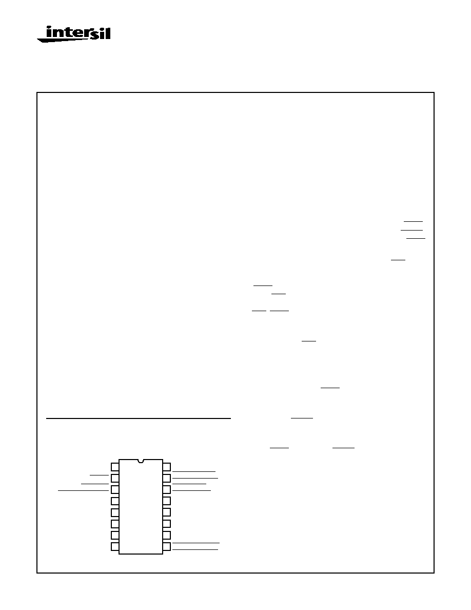
Pinout
CD40102BMS, CD40130BMS
TOP VIEW
14
15
16
9
13
12
11
10
1
2
3
4
5
7
6
8
CLOCK
CLEAR
CARRY IN/
J0
J1
J2
VSS
J3
VDD
CARRY OUT/
J7
J6
J5
J4
ASYNCHRONOUS
SYNCHRONOUS
COUNTER ENABLE
PRESET ENABLE
ZERO DETECT
PRESET ENABLE
File Number
3351
December 1992
7-1295
Specifications CD40102BMS, CD40103BMS
Absolute Maximum Ratings
Reliability Information
DC Supply Voltage Range, (VDD) . . . . . . . . . . . . . . . -0.5V to +20V
(Voltage Referenced to VSS Terminals)
Input Voltage Range, All Inputs . . . . . . . . . . . . .-0.5V to VDD +0.5V
DC Input Current, Any One Input
. . . . . . . . . . . . . . . . . . . . . . . .±
10mA
Operating Temperature Range . . . . . . . . . . . . . . . . -55
o
C to +125
o
C
Package Types D, F, K, H
Storage Temperature Range (TSTG) . . . . . . . . . . . -65
o
C to +150
o
C
Lead Temperature (During Soldering) . . . . . . . . . . . . . . . . . +265
o
C
At Distance 1/16
±
1/32 Inch (1.59mm
±
0.79mm) from case for
10s Maximum
Thermal Resistance
ja
jc
Ceramic DIP Package . . . . . . . . . . . . .
80
o
C/W
20
o
C/W
Flatpack Package . . . . . . . . . . . . . . . .
70
o
C/W
20
o
C/W
Maximum Package Power Dissipation (PD) at +125
o
C
For T
A
= -55
o
C to +100
o
C (Package Type D, F, K) . . . . . . 500mW
For T
A
= +100
o
C to +125
o
C (Package Type D, F, K). . . . . . Derate
Linearity at 12mW/
o
C to 200mW
Device Dissipation per Output Transistor . . . . . . . . . . . . . . . 100mW
For T
A
= Full Package Temperature Range (All Package Types)
Junction Temperature . . . . . . . . . . . . . . . . . . . . . . . . . . . . . . +175
o
C
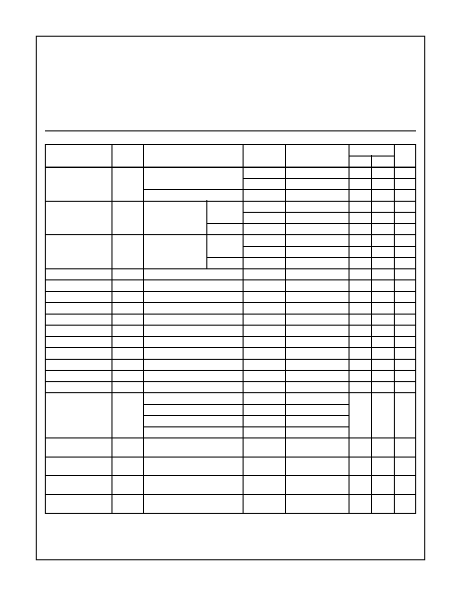
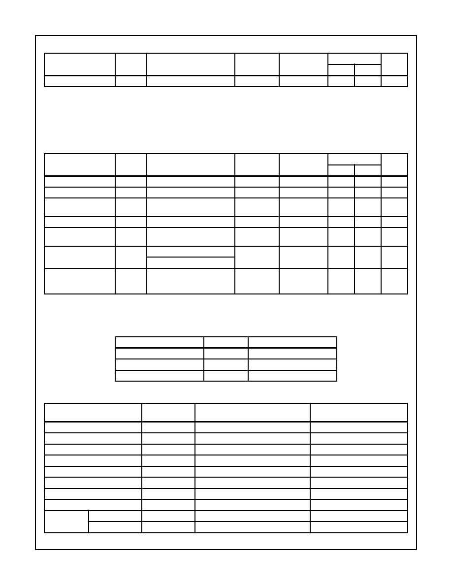
TABLE 1. DC ELECTRICAL PERFORMANCE CHARACTERISTICS
PARAMETER
SYMBOL
CONDITIONS (NOTE 1)
GROUP A
SUBGROUPS
TEMPERATURE
LIMITS
UNITS
MIN
MAX
Supply Current
IDD
VDD = 20V, VIN = VDD or GND
1
+25
o
C
-
10
µ
A
2
+125
o
C
-
1000
µ
A
VDD = 18V, VIN = VDD or GND
3
-55
o
C
-
10
µ
A
Input Leakage Current
IIL
VIN = VDD or GND
VDD = 20V
1
+25
o
C
-100
-
nA
2
+125
o
C
-1000
-
nA
VDD = 18V
3
-55
o
C
-100
-
nA
Input Leakage Current
IIH
VIN = VDD or GND
VDD = 20V
1
+25
o
C
-
100
nA
2
+125
o
C
-
1000
nA
VDD = 18V
3
-55
o
C
-
100
nA
Output Voltage
VOL15
VDD = 15V, No Load
1, 2, 3
+25
o
C, +125
o
C, -55
o
C
-
50
mV
Output Voltage
VOH15
VDD = 15V, No Load (Note 3)
1, 2, 3
+25
o
C, +125
o
C, -55
o
C 14.95
-
V
Output Current (Sink)
IOL5
VDD = 5V, VOUT = 0.4V
1
+25
o
C
0.53
-
mA
Output Current (Sink)
IOL10
VDD = 10V, VOUT = 0.5V
1
+25
o
C
1.4
-
mA
Output Current (Sink)
IOL15
VDD = 15V, VOUT = 1.5V
1
+25
o
C
3.5
-
mA
Output Current (Source)
IOH5A
VDD = 5V, VOUT = 4.6V
1
+25
o
C
-
-0.53
mA
Output Current (Source)
IOH5B
VDD = 5V, VOUT = 2.5V
1
+25
o
C
-
-1.8
mA
Output Current (Source)
IOH10
VDD = 10V, VOUT = 9.5V
1
+25
o
C
-
-1.4
mA
Output Current (Source)
IOH15
VDD = 15V, VOUT = 13.5V
1
+25
o
C
-
-3.5
mA
N Threshold Voltage
VNTH
VDD = 10V, ISS = -10
µ
A
1
+25
o
C
-2.8
-0.7
V
P Threshold Voltage
VPTH
VSS = 0V, IDD = 10
µ
A
1
+25
o
C
0.7
2.8
V
Functional
F
VDD = 2.8V, VIN = VDD or GND
7
+25
o
C
VOH >
VDD/2
VOL <
VDD/2
V
VDD = 20V, VIN = VDD or GND
7
+25
o
C
VDD = 18V, VIN = VDD or GND
8A
+125
o
C
VDD = 3V, VIN = VDD or GND
8B
-55
o
C
Input Voltage Low
(Note 2)
VIL
VDD = 5V, VOH > 4.5V, VOL < 0.5V
1, 2, 3
+25
o
C, +125
o
C, -55
o
C
-
1.5
V
Input Voltage High
(Note 2)
VIH
VDD = 5V, VOH > 4.5V, VOL < 0.5V
1, 2, 3
+25
o
C, +125
o
C, -55
o
C
3.5
-
V
Input Voltage Low
(Note 2)
VIL
VDD = 15V, VOH > 13.5V,
VOL < 1.5V
1, 2, 3
+25
o
C, +125
o
C, -55
o
C
-
4
V
Input Voltage High
(Note 2)
VIH
VDD = 15V, VOH > 13.5V,
VOL < 1.5V
1, 2, 3
+25
o
C, +125
o
C, -55
o
C
11
-
V
NOTES: 1. All voltages referenced to device GND, 100% testing being
implemented.
2. Go/No Go test with limits applied to inputs.
3. For accuracy, voltage is measured differentially to VDD. Limit
is 0.050V max.
7-1296
Specifications CD40102BMS, CD40103BMS
TABLE 2. AC ELECTRICAL PERFORMANCE CHARACTERISTICS
PARAMETER
SYMBOL
CONDITIONS (NOTE 1, 2)
GROUP A
SUBGROUPS
TEMPERATURE
LIMITS
UNITS
MIN
MAX
Propagation Delay
Clock to Output
TPHL1
TPLH1
VDD = 5V, VIN = VDD or GND
9
+25
o
C
-
600
ns
10, 11
+125
o
C, -55
o
C
-
810
ns
Propagation Delay
Carry In/Counter Enable
to Output
TPHL2
TPLH2
VDD = 5V, VIN = VDD or GND
9
+25
o
C
-
400
ns
10, 11
+125
o
C, -55
o
C
-
540
ns
Propagation Delay
Asynchronous Preset
Enable to Output
TPHL3
TPLH3
VDD = 5V, VIN = VDD or GND
9
+25
o
C
-
1300
ns
10, 11
+125
o
C, -55
o
C
-
1755
ns
Propagation Delay
Clear to Output
TPLH4
VDD = 5V, VIN = VDD or GND
9
+25
o
C
-
750
ns
10, 11
+125
o
C, -55
o
C
-
1012
ns
Transition Time
TTHL
TTLH
VDD = 5V, VIN = VDD or GND
9
+25
o
C
-
200
ns
10, 11
+125
o
C, -55
o
C
-
270
ns
Maximum Clock Input
Frequency
FCL
VDD = 5V, VIN = VDD or GND
9
+25
o
C
.7
-
MHz
10, 11
+125
o
C, -55
o
C
.52
-
MHz
NOTES:
1. CL = 50pF, RL = 200K, Input TR, TF < 20ns.
2. -55
o
C and +125
o
C limits guaranteed, 100% testing being implemented.
TABLE 3. ELECTRICAL PERFORMANCE CHARACTERISTICS
PARAMETER
SYMBOL
CONDITIONS
NOTES
TEMPERATURE
LIMITS
UNITS
MIN
MAX
Supply Current
IDD
VDD = 5V, VIN = VDD or GND
1, 2
-55
o
C, +25
o
C
-
5
µ
A
+125
o
C
-
150
µ
A
VDD = 10V, VIN = VDD or GND
1, 2
-55
o
C, +25
o
C
-
10
µ
A
+125
o
C
-
300
µ
A
VDD = 15V, VIN = VDD or GND
1, 2
-55
o
C, +25
o
C
-
10
µ
A
+125
o
C
-
600
µ
A
Output Voltage
VOL
VDD = 5V, No Load
1, 2
+25
o
C, +125
o
C,
-55
o
C
-
50
mV
Output Voltage
VOL
VDD = 10V, No Load
1, 2
+25
o
C, +125
o
C,
-55
o
C
-
50
mV
Output Voltage
VOH
VDD = 5V, No Load
1, 2
+25
o
C, +125
o
C,
-55
o
C
4.95
-
V
Output Voltage
VOH
VDD = 10V, No Load
1, 2
+25
o
C, +125
o
C,
-55
o
C
9.95
-
V
Output Current (Sink)
IOL5
VDD = 5V, VOUT = 0.4V
1, 2
+125
o
C
0.36
-
mA
-55
o
C
0.64
-
mA
Output Current (Sink)
IOL10
VDD = 10V, VOUT = 0.5V
1, 2
+125
o
C
0.9
-
mA
-55
o
C
1.6
-
mA
Output Current (Sink)
IOL15
VDD = 15V, VOUT = 1.5V
1, 2
+125
o
C
2.4
-
mA
-55
o
C
4.2
-
mA
Output Current (Source)
IOH5A
VDD = 5V, VOUT = 4.6V
1, 2
+125
o
C
-
-0.36
mA
-55
o
C
-
-0.64
mA
Output Current (Source)
IOH5B
VDD = 5V, VOUT = 2.5V
1, 2
+125
o
C
-
-1.15
mA
-55
o
C
-
-2.0
mA
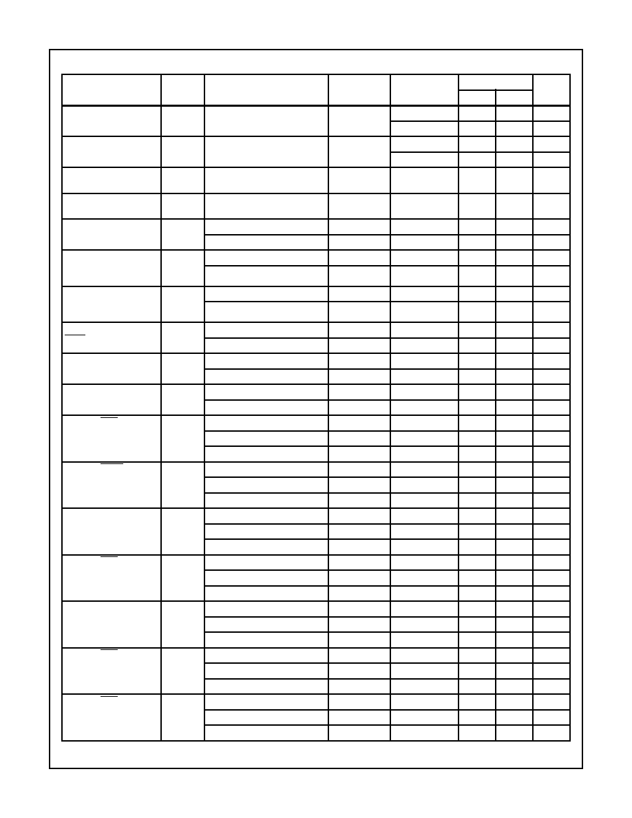
7-1297
Specifications CD40102BMS, CD40103BMS
Output Current (Source)
IOH10
VDD = 10V, VOUT = 9.5V
1, 2
+125
o
C
-
-0.9
mA
-55
o
C
-
-1.6
mA
Output Current (Source)
IOH15
VDD =15V, VOUT = 13.5V
1, 2
+125
o
C
-
-2.4
mA
-55
o
C
-
-4.2
mA
Input Voltage Low
VIL
VDD = 10V, VOH > 9V, VOL < 1V
1, 2
+25
o
C, +125
o
C,
-55
o
C
-
3
V
Input Voltage High
VIH
VDD = 10V, VOH > 9V, VOL < 1V
1, 2
+25
o
C, +125
o
C,
-55
o
C
7
-
V
Propagation Delay
Clock to Output
TPHL1
TPLH1
VDD = 10V
1, 2, 3
+25
o
C
-
260
ns
VDD = 15V
1, 2, 3
+25
o
C
-
190
ns
Propagation Delay
Carry In/Counter Enable
to Output
TPHL2
TPLH2
VDD = 10V
1, 2, 3
+25
o
C
-
180
ns
VDD = 15V
1, 2, 3
+25
o
C
-
130
ns
Propagation Delay
Asynchronous Preset En-
able to Output
TPHL3
TPLH3
VDD = 10V
1, 2, 3
+25
o
C
-
600
ns
VDD = 15V
1, 2, 3
+25
o
C
-
400
ns
Propagation Delay
Clear to Output
TPLH4
VDD = 10V
1, 2, 3
+25
o
C
-
360
ns
VDD = 15V
1, 2, 3
+25
o
C
-
200
ns
Transition Time
TTHL1
TTLH1
VDD = 10V
1, 2, 3
+25
o
C
-
100
ns
VDD = 15V
1, 2, 3
+25
o
C
-
80
ns
Maximum Clock Input
Frequency
FCL
VDD = 10V
1, 2
+25
o
C
1.8
-
MHz
VDD = 15V
1, 2
+25
o
C
2.4
-
MHz
Minimum SPE Setup
Time
TSU
VDD = 5V
1, 2, 3
+25
o
C
-
280
ns
VDD = 10V
1, 2, 3
+25
o
C
-
140
ns
VDD = 15V
1, 2, 3
+25
o
C
-
100
ns
Minimum CI/CE Setup
Time
TSU
VDD = 5V
1, 2, 3
+25
o
C
-
500
ns
VDD = 10V
1, 2, 3
+25
o
C
-
250
ns
VDD = 15V
1, 2, 3
+25
o
C
-
150
ns
Minimum Clock Pulse
Width
TW
VDD = 5V
1, 2, 3
+25
o
C
-
300
ns
VDD = 10V
1, 2, 3
+25
o
C
-
180
ns
VDD = 15V
1, 2, 3
+25
o
C
-
80
ns
Minimum APE Pulse
Width
TW
VDD = 5V
1, 2, 3
+25
o
C
-
360
ns
VDD = 10V
1, 2, 3
+25
o
C
-
160
ns
VDD = 15V
1, 2, 3
+25
o
C
-
120
ns
Minimum JAM Setup
Time (Synchronous Pre-
setting)
TSU
VDD = 5V
1, 2, 3
+25
o
C
-
200
ns
VDD = 10V
1, 2, 3
+25
o
C
-
80
ns
VDD = 15V
1, 2, 3
+25
o
C
-
60
ns
Minimum APE Removal
Time
TREM
VDD = 5V
1, 2, 3
+25
o
C
-
220
ns
VDD = 10V
1, 2, 3
+25
o
C
-
100
ns
VDD = 15V
1, 2, 3
+25
o
C
-
70
ns
Minimum CLR Pulse
Width
TW
VDD = 5V
1, 2, 3
+25
o
C
-
320
ns
VDD = 10V
1, 2, 3
+25
o
C
-
160
ns
VDD = 15V
1, 2, 3
+25
o
C
-
100
ns
TABLE 3. ELECTRICAL PERFORMANCE CHARACTERISTICS (Continued)
PARAMETER
SYMBOL
CONDITIONS
NOTES
TEMPERATURE
LIMITS
UNITS
MIN
MAX
7-1298
Specifications CD40102BMS, CD40103BMS
Input Capacitance
CIN
Any Input
1, 2
+25
o
C
-
7.5
pF
NOTES:
1. All voltages referenced to device GND.
2. The parameters listed on Table 3 are controlled via design or process and are not directly tested. These parameters are characterized
on initial design release and upon design changes which would affect these characteristics.
3. CL = 50pF, RL = 200K, Input TR, TF < 20ns.
TABLE 4. POST IRRADIATION ELECTRICAL PERFORMANCE CHARACTERISTICS
PARAMETER
SYMBOL
CONDITIONS
NOTES
TEMPERATURE
LIMITS
UNITS
MIN
MAX
Supply Current
IDD
VDD = 20V, VIN = VDD or GND
1, 4
+25
o
C
-
25
µ
A
N Threshold Voltage
VNTH
VDD = 10V, ISS = -10
µ
A
1, 4
+25
o
C
-2.8
-0.2
V
N Threshold Voltage
Delta
VTN
VDD = 10V, ISS = -10
µ
A
1, 4
+25
o
C
-
±
1
V
P Threshold Voltage
VTP
VSS = 0V, IDD = 10
µ
A
1, 4
+25
o
C
0.2
2.8
V
P Threshold Voltage
Delta
VTP
VSS = 0V, IDD = 10
µ
A
1, 4
+25
o
C
-
±
1
V
Functional
F
VDD = 18V, VIN = VDD or GND
1
+25
o
C
VOH >
VDD/2
VOL <
VDD/2
V
VDD = 3V, VIN = VDD or GND
Propagation Delay Time
TPHL
TPLH
VDD = 5V
1, 2, 3, 4
+25
o
C
-
1.35 x
+25
o
C
Limit
ns
NOTES: 1. All voltages referenced to device GND.
2. CL = 50pF, RL = 200K, Input TR, TF < 20ns.
3. See Table 2 for +25
o
C limit.
4. Read and Record
TABLE 5. BURN-IN AND LIFE TEST DELTA PARAMETERS +25
o
C
PARAMETER
SYMBOL
DELTA LIMIT
Supply Current - MSI-2
IDD
±
1.0
µ
A
Output Current (Sink)
IOL5
±
20% x Pre-Test Reading
Output Current (Source)
IOH5A
±
20% x Pre-Test Reading
TABLE 6. APPLICABLE SUBGROUPS
CONFORMANCE GROUP
MIL-STD-883
METHOD
GROUP A SUBGROUPS
READ AND RECORD
Initial Test (Pre Burn-In)
100% 5004
1, 7, 9
IDD, IOL5, IOH5A
Interim Test 1 (Post Burn-In)
100% 5004
1, 7, 9
IDD, IOL5, IOH5A
Interim Test 2 (Post Burn-In)
100% 5004
1, 7, 9
IDD, IOL5, IOH5A
PDA (Note 1)
100% 5004
1, 7, 9, Deltas
Interim Test 3 (Post Burn-In)
100% 5004
1, 7, 9
IDD, IOL5, IOH5A
PDA (Note 1)
100% 5004
1, 7, 9, Deltas
Final Test
100% 5004
2, 3, 8A, 8B, 10, 11
Group A
Sample 5005
1, 2, 3, 7, 8A, 8B, 9, 10, 11
Group B
Subgroup B-5
Sample 5005
1, 2, 3, 7, 8A, 8B, 9, 10, 11, Deltas
Subgroups 1, 2, 3, 9, 10, 11
Subgroup B-6
Sample 5005
1, 7, 9
TABLE 3. ELECTRICAL PERFORMANCE CHARACTERISTICS (Continued)
PARAMETER
SYMBOL
CONDITIONS
NOTES
TEMPERATURE
LIMITS
UNITS
MIN
MAX