 | –≠–ª–µ–∫—Ç—Ä–æ–Ω–Ω—ã–π –∫–æ–º–ø–æ–Ω–µ–Ω—Ç: CD40105 | –°–∫–∞—á–∞—Ç—å:  PDF PDF  ZIP ZIP |
7-1317
CAUTION: These devices are sensitive to electrostatic discharge; follow proper IC Handling Procedures.
1-888-INTERSIL or 321-724-7143 | Copyright © Intersil Corporation 1999
CD40105BMS
CMOS FIFO Register
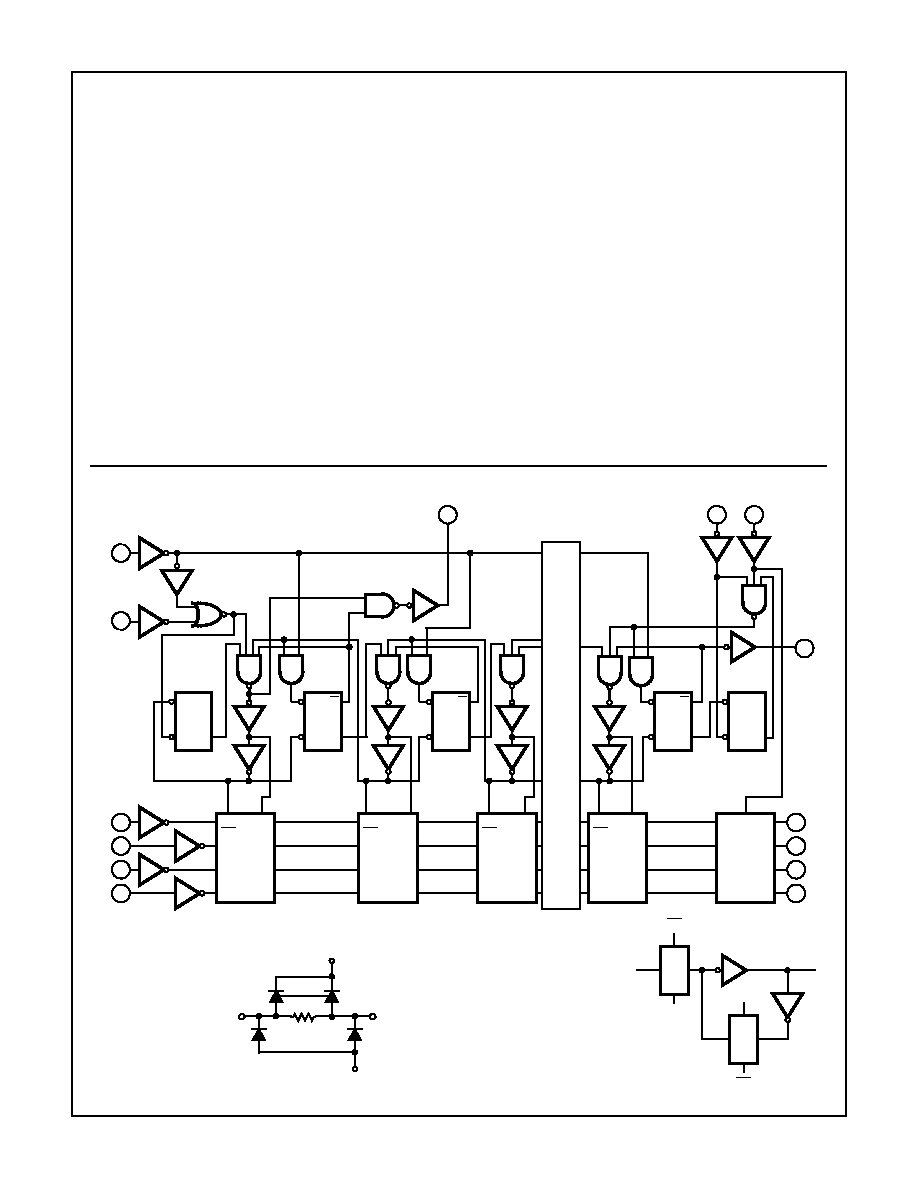
Description
CD40105BMS is a low-power first-in-first-out (FIFO) "elastic"
storage register that can store 16 4-bit words. It is capable of
handling input and output data at different shifting rates. This
feature makes it particularly useful as a buffer between asyn-
chronous systems.
Each word position in the register is clocked by a control flip-
flop, which stores a marker bit. A "1" signifies that the posi-
tion's data is filled and a "0" denotes a vacancy in that posi-
tion. The control flip-flop detects the state of the preceding
flip-flop and communicates its own status to the succeeding
flip-flop. When a control flip-flop is in the "0" state and sees a
"1" in the preceding flip-flop, it generates a clock pulse that
transfers data from the preceding four data latches into its
own four data latches and resets the preceding flip-flop to
"0". The first and last control flip-flops have buffered outputs.
Since all empty locations "bubble" automatically to the input
end, and all valid data ripple through to the output end, the
status of the first control flip-flop (DATA-IN READY) indicates
if the FIFO is full, and the status of the last flip-flop (DATA-
OUT READY) indicates if the FIFO contains data. As the
earliest data are removed from the bottom of the data stack
(the output end), all data entered later will automatically
propagate (ripple) toward the output.
Loading Data - Data can be entered whenever the DATA-IN
READY (DIR) flag is high, by a low to high transition on the
SHIFT-IN (SI) input. This input must go low momentarily
before the next word is accepted by the FIFO. The DIR flag
will go low momentarily, until that data have been transferred
to the second location. The flag will remain low when all 16-
word locations are filled with valid data, and further pulses
on the SI input will be ignored until DIR goes high.
Features
∑ 4 Bits x 16 Words
∑ High Voltage Type (20V Rating)
∑ Independent Asynchronous Inputs and Outputs
∑ 3-State Outputs
∑ Expandable in Either Direction
∑ Status Indicators on Input and Output
∑ Reset Capability
∑ Standardized Symmetrical Output Characteristics
∑ 100% Tested for Quiescent Current at 20V
∑ 5V, 10V and 15V Parametric Ratings
∑ Maximum Input Current of 1
µ
A at 18V Over Full Pack-
age Temperature Range; 100nA at 18V and +25
o
C
∑ Noise Margin (Over Full Package/Temperature Range)
- 1V at VDD = 5V
- 2V at VDD = 10V
- 2.5V at VDD = 15V
∑ Meets All Requirements of JEDEC Tentative Standard
No. 13B, "Standard Specifications for Description of
`B' Series CMOS Devices"
Applications
∑ Bit Rate Smoothing
∑ CPU/Terminal Buffering
∑ Data Communications
∑ Peripheral Buffering
∑ Line Printer Input Buffers
∑ Auto Dialers
∑ CRT Buffer Memories
∑ Radar Data Acquisition
December 1992
File Number
3353
Continued on next page
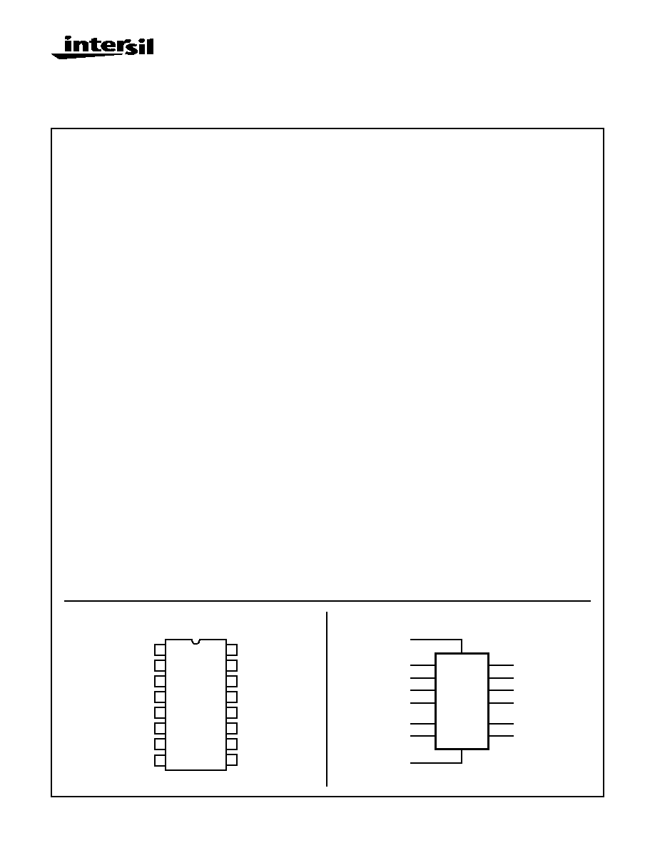
Pinout
CD40105BMS
TOP VIEW
14
15
16
9
13
12
11
10
1
2
3
4
5
7
6
8
3 - STATE
DIR
SI
D0
D1
D2
VSS
D3
VDD
DOR
Q0
Q1
Q2
Q3
MR
SO
CONTROL
Functional Diagram
13
12
11
10
14
2
Q0
Q1
Q2
Q3
DATA-OUT
READY
DATA-IN
READY
4
5
6
7
3
15
D0
D1
D2
D3
SHIFT IN
SHIFT OUT
1
9
3-STATE
CONTROL
MASTER
RESET
VDD = 16
VSS = 8
7-1318
CD40105BMS
Unloading Data - As soon as the first word has rippled to
the output, DATA-OUT READY (DOR) goes high, and data
can be removed by a falling edge on the SO input. This fall-
ing edge causes the DOR signal to go low while the word on
the output is dumped and the next word moves to the output.
As long as valid data are available in the FIFO, the DOR sig-
nal will go high again signifying that the next word is ready at
the output. When the FIFO is empty, DOR will remain low,
and any further commands will be ignored until a "1" marker
ripples down to the last control register, when DOR goes
high. Unloading of data is inhibited while the 3-state control
input is high. The 3-state control signal should not be shifted
from high to low (data outputs turned on) while the SHIFT-
OUT is at logic 0. This level change would cause the first
word to be shifted out (unloaded) immediately and the data
to be lost.
Cascading - The CD40105BMS can be cascaded to form
longer registers simply by connecting the DIR to SO and
DOR to SI. In the cascaded mode, a MASTER RESET pulse
must be applied after the supply voltage is turned on. For
words wider than 4 bits, the DIR and the DOR outputs must
be gated together with AND gates. Their outputs drive the SI
and SO inputs in parallel, if expanding is done in both direc-
tions (see Figures 9 and 11).
3-State Outputs - In order to facilitate data busing, 3-state
outputs are provided on the data output lines, while the load
condition of the register can be detected by the state of the
DOR output.
Master Reset - A high on the MASTER RESET (MR) sets all
the control logic marker bits to "0". DOR goes low and DIR
goes high. The contents of the data register are not
changed, only declared invalid, and will be superseded when
the first word is loaded. The shift-in must be low during Mas-
ter Reset.
The CD40105BMS is supplied in these 16-lead outline pack-
ages:
Braze Seal DIP
H4X
Frit Seal DIP
H1F
Ceramic Flatpack
H6W
Logic Diagram
CL
CL
2
15
1
9
3
4
5
6
7
R
S
Q
R
S
Q
Q
1
R
S
Q
Q
2
POSITIONS
4 - 15
R
S
Q
Q
16
R
S
Q
CL
4
LATCHES
CL
CL
4
LATCHES
CL
CL
4
LATCHES
CL
CL
4
LATCHES
CL
3
STATE
OUTPUT
BUFFERS
13
12
11
10
*
*
*
*
*
*
*
ALL INPUTS PROTECTED BY
COS/MOS PROTECTION
NETWORK
POS 1
POS 2
POS 3
POS 16
MASTER
RESET
SHIFT
IN
D0
D1
D2
D3
DATA IN READY
(DIR)
SHIFT
OUT
3 - STATE
CONTROL
(OUTPUT
ENABLE)
DATA
READY
(DOR)
Q0
Q1
Q2
Q3
*
*
VDD
VSS
p
n
CL
CL
p
n
DETAIL OF LATCHES
14
7-1319
Specifications CD40105BMS
Absolute Maximum Ratings
Reliability Information
DC Supply Voltage Range, (VDD) . . . . . . . . . . . . . . . -0.5V to +20V
(Voltage Referenced to VSS Terminals)
Input Voltage Range, All Inputs . . . . . . . . . . . . .-0.5V to VDD +0.5V
DC Input Current, Any One Input
. . . . . . . . . . . . . . . . . . . . . . . .±
10mA
Operating Temperature Range . . . . . . . . . . . . . . . . -55
o
C to +125
o
C
Package Types D, F, K, H
Storage Temperature Range (TSTG) . . . . . . . . . . . -65
o
C to +150
o
C
Lead Temperature (During Soldering) . . . . . . . . . . . . . . . . . +265
o
C
At Distance 1/16
±
1/32 Inch (1.59mm
±
0.79mm) from case for
10s Maximum
Thermal Resistance . . . . . . . . . . . . . . . .
ja
jc
Ceramic DIP and FRIT Package . . . . .
80
o
C/W
20
o
C/W
Flatpack Package . . . . . . . . . . . . . . . .
70
o
C/W
20
o
C/W
Maximum Package Power Dissipation (PD) at +125
o
C
For T
A
= -55
o
C to +100
o
C (Package Type D, F, K) . . . . . . 500mW
For T
A
= +100
o
C to +125
o
C (Package Type D, F, K). . . . . . Derate
Linearity at 12mW/
o
C to 200mW
Device Dissipation per Output Transistor . . . . . . . . . . . . . . . 100mW
For T
A
= Full Package Temperature Range (All Package Types)
Junction Temperature . . . . . . . . . . . . . . . . . . . . . . . . . . . . . . +175
o
C
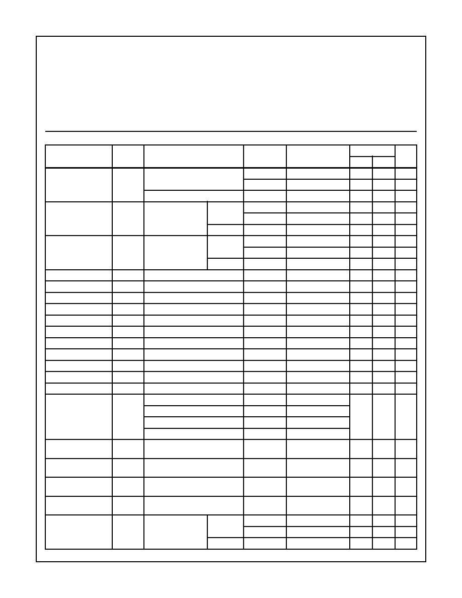
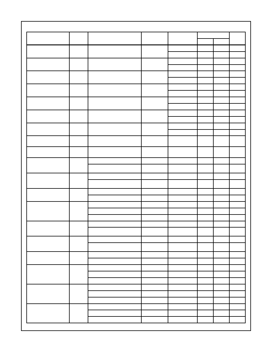
TABLE 1. DC ELECTRICAL PERFORMANCE CHARACTERISTICS
PARAMETER
SYMBOL
CONDITIONS (NOTE 1)
GROUP A
SUBGROUPS
TEMPERATURE
LIMITS
UNITS
MIN
MAX
Supply Current
IDD
VDD = 20V, VIN = VDD or GND
1
+25
o
C
-
10
µ
A
2
+125
o
C
-
1000
µ
A
VDD = 18V, VIN = VDD or GND
3
-55
o
C
-
10
µ
A
Input Leakage Current
IIL
VIN = VDD or GND
VDD = 20
1
+25
o
C
-100
-
nA
2
+125
o
C
-1000
-
nA
VDD = 18V
3
-55
o
C
-100
-
nA
Input Leakage Current
IIH
VIN = VDD or GND
VDD = 20
1
+25
o
C
-
100
nA
2
+125
o
C
-
1000
nA
VDD = 18V
3
-55
o
C
-
100
nA
Output Voltage
VOL15
VDD = 15V, No Load
1, 2, 3
+25
o
C, +125
o
C, -55
o
C
-
50
mV
Output Voltage
VOH15
VDD = 15V, No Load (Note 3)
1, 2, 3
+25
o
C, +125
o
C, -55
o
C 14.95
-
V
Output Current (Sink)
IOL5
VDD = 5V, VOUT = 0.4V
1
+25
o
C
0.53
-
mA
Output Current (Sink)
IOL10
VDD = 10V, VOUT = 0.5V
1
+25
o
C
1.4
-
mA
Output Current (Sink)
IOL15
VDD = 15V, VOUT = 1.5V
1
+25
o
C
3.5
-
mA
Output Current (Source)
IOH5A
VDD = 5V, VOUT = 4.6V
1
+25
o
C
-
-0.53
mA
Output Current (Source)
IOH5B
VDD = 5V, VOUT = 2.5V
1
+25
o
C
-
-1.8
mA
Output Current (Source)
IOH10
VDD = 10V, VOUT = 9.5V
1
+25
o
C
-
-1.4
mA
Output Current (Source)
IOH15
VDD = 15V, VOUT = 13.5V
1
+25
o
C
-
-3.5
mA
N Threshold Voltage
VNTH
VDD = 10V, ISS = -10
µ
A
1
+25
o
C
-2.8
-0.7
V
P Threshold Voltage
VPTH
VSS = 0V, IDD = 10
µ
A
1
+25
o
C
0.7
2.8
V
Functional
(Note 4)
F
VDD = 2.8V, VIN = VDD or GND
7
+25
o
C
VOH >
VDD/2
VOL <
VDD/2
V
VDD = 20V, VIN = VDD or GND
7
+25
o
C
VDD = 18V, VIN = VDD or GND
8A
+125
o
C
VDD = 3V, VIN = VDD or GND
8B
-55
o
C
Input Voltage Low
(Note 2)
VIL
VDD = 5V, VOH > 4.5V, VOL < 0.5V
1, 2, 3
+25
o
C, +125
o
C, -55
o
C
-
1.5
V
Input Voltage High
(Note 2)
VIH
VDD = 5V, VOH > 4.5V, VOL < 0.5V
1, 2, 3
+25
o
C, +125
o
C, -55
o
C
3.5
-
V
Input Voltage Low (Note
2)
VIL
VDD = 15V, VOH > 13.5V, VOL < 1.5V
1, 2, 3
+25
o
C, +125
o
C, -55
o
C
-
4
V
Input Voltage High
(Note 2)
VIH
VDD = 15V, VOH > 13.5V, VOL < 1.5V
1, 2, 3
+25
o
C, +125
o
C, -55
o
C
11
-
V
Tri-State Output
Leakage
IOZL
VIN = VDD or GND
VOUT = 0V
VDD = 20V
1
+25
o
C
-0.4
-
µ
A
2
+125
o
C
-12
-
µ
A
VDD = 18V
3
-55
o
C
-0.4
-
µ
A
7-1320
Specifications CD40105BMS
Tri-State Output
Leakage
IOZH
VIN = VDD or GND
VOUT = VDD
VDD = 20V
1
+25
o
C
-
0.4
µ
A
2
+125
o
C
-
12
µ
A
VDD = 18V
3
-55
o
C
-
0.4
µ
A
NOTES: 1. All voltages referenced to device GND, 100% testing being
implemented.
2. Go/No Go test with limits applied to inputs.
3. For accuracy, voltage is measured differentially to VDD. Limit
is 0.050V max.
4. VDD = 2.8V/3.0V, RL = 100K to VDD
VDD = 20V/18V, RL = 10K to VDD
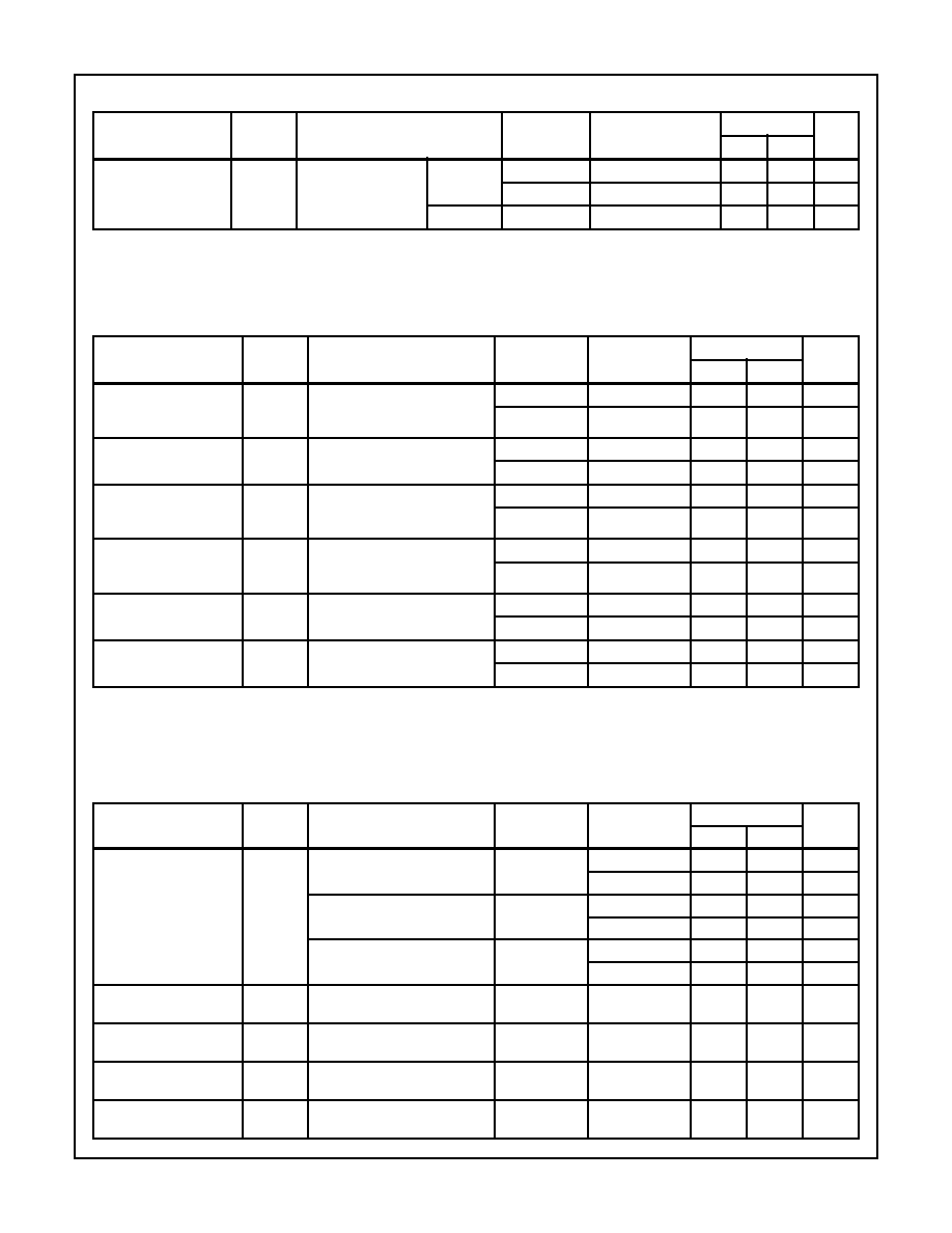
TABLE 2. AC ELECTRICAL PERFORMANCE CHARACTERISTICS
PARAMETER
SYMBOL
CONDITIONS (NOTE 1)
GROUP A
SUBGROUPS
TEMPERATURE
LIMITS
UNITS
MIN
MAX
Propagation Delay
Shift Out or Reset to
Data-Out Ready
TPHL1
VDD = 5V, VIN = VDD or GND
(Note 1, 2)
9
+25
o
C
-
370
ns
10, 11
+125
o
C, -55
o
C
-
500
ns
Propagation Delay
Shift In to Data-In Ready
TPHL2
VDD = 5V, VIN = VDD or GND
(Note 1, 2)
9
+25
o
C
-
320
ns
10, 11
+125
o
C, -55
o
C
-
432
ns
Propagation Delay
Ripple through Delay In-
put to Output
TPLH3
VDD = 5V, VIN = VDD or GND
(Note 1, 2)
9
+25
o
C
-
4
µ
s
10, 11
+125
o
C, -55
o
C
-
5.4
µ
s
Propagation Delay
3-State Control to Data
Out
TPZH
VDD = 5V, VIN = VDD or GND
(Note 2, 3)
9
+25
o
C
-
280
ns
10, 11
+125
o
C, -55
o
C
-
378
ns
Transition Time
TTHL
TTLH
VDD = 5V, VIN = VDD or GND
(Note 1, 2)
9
+25
o
C
-
200
ns
10, 11
+125
o
C, -55
o
C
-
270
ns
Maximum Shift-In or
Shift-Out Rate
FCL
VDD = 5V (Note 1, 2),
VIN = VDD or GND
9
+25
o
C
1.5
-
MHz
10, 11
+125
o
C, -55
o
C
1.11
-
MHz
NOTES:
1. CL = 50pF, RL = 200K, Input TR, TF < 20ns.
2. -55
o
C and +125
o
C limits guaranteed, 100% testing being implemented.
3. CL = 50pF, RL = 1K, Input TR, TF < 20ns.
TABLE 3. ELECTRICAL PERFORMANCE CHARACTERISTICS
PARAMETER
SYMBOL
CONDITIONS
NOTES
TEMPERATURE
LIMITS
UNITS
MIN
MAX
Supply Current
IDD
VDD = 5V, VIN = VDD or GND
1, 2
-55
o
C, +25
o
C
-
5
µ
A
+125
o
C
-
150
µ
A
VDD = 10V, VIN = VDD or GND
1, 2
-55
o
C, +25
o
C
-
10
µ
A
+125
o
C
-
300
µ
A
VDD = 15V, VIN = VDD or GND
1, 2
-55
o
C, +25
o
C
-
10
µ
A
+125
o
C
-
600
µ
A
Output Voltage
VOL
VDD = 5V, No Load
1, 2
+25
o
C, +125
o
C,
-55
o
C
-
50
mV
Output Voltage
VOL
VDD = 10V, No Load
1, 2
+25
o
C, +125
o
C,
-55
o
C
-
50
mV
Output Voltage
VOH
VDD = 5V, No Load
1, 2
+25
o
C, +125
o
C,
-55
o
C
4.95
-
V
Output Voltage
VOH
VDD = 10V, No Load
1, 2
+25
o
C, +125
o
C,
-55
o
C
9.95
-
V
TABLE 1. DC ELECTRICAL PERFORMANCE CHARACTERISTICS
PARAMETER
SYMBOL
CONDITIONS (NOTE 1)
GROUP A
SUBGROUPS
TEMPERATURE
LIMITS
UNITS
MIN
MAX
7-1321
Specifications CD40105BMS
Output Current (Sink)
IOL5
VDD = 5V, VOUT = 0.4V
1, 2
+125
o
C
0.36
-
mA
-55
o
C
0.64
-
mA
Output Current (Sink)
IOL10
VDD = 10V, VOUT = 0.5V
1, 2
+125
o
C
0.9
-
mA
-55
o
C
1.6
-
mA
Output Current (Sink)
IOL15
VDD = 15V, VOUT = 1.5V
1, 2
+125
o
C
2.4
-
mA
-55
o
C
4.2
-
mA
Output Current (Source)
IOH5A
VDD = 5V, VOUT = 4.6V
1, 2
+125
o
C
-
-0.36
mA
-55
o
C
-
-0.64
mA
Output Current (Source)
IOH5B
VDD = 5V, VOUT = 2.5V
1, 2
+125
o
C
-
-1.15
mA
-55
o
C
-
-2.0
mA
Output Current (Source)
IOH10
VDD = 10V, VOUT = 9.5V
1, 2
+125
o
C
-
-0.9
mA
-55
o
C
-
-1.6
mA
Output Current (Source)
IOH15
VDD =15V, VOUT = 13.5V
1, 2
+125
o
C
-
-2.4
mA
-55
o
C
-
-4.2
mA
Input Voltage Low
VIL
VDD = 10V, VOH > 9V, VOL < 1V
1, 2
+25
o
C, +125
o
C,
-55
o
C
-
3
V
Input Voltage High
VIH
VDD = 10V, VOH > 9V, VOL < 1V
1, 2
+25
o
C, +125
o
C,
-55
o
C
7
-
V
Propagation Delay
Shift or Reset to Data Out
Ready
TPHL1
VDD = 10V
1, 2, 3
+25
o
C
-
180
ns
VDD = 15V
1, 2, 3
+25
o
C
-
130
ns
Propagation Delay Ripple
through Delay Input to
Output
TPLH3
VDD = 10V
1, 2, 3
+25
o
C
-
2
µ
s
VDD = 15V
1, 2, 3
+25
o
C
-
1.4
µ
s
Propagation Delay
Shift-In to Data-In Ready
TPHL2
VDD = 10V
1, 2, 3
+25
o
C
-
130
ns
VDD = 15V
1, 2, 3
+25
o
C
-
90
ns
Propagation Delay
Shift Out to QN Out
TPHL4
TPLH4
VDD = 5V
1, 2, 3
+25
o
C
-
420
ns
VDD = 10V
1, 2, 3
+25
o
C
-
380
ns
VDD = 15V
1, 2, 3
+25
o
C
-
250
ns
Propagation Delay
3-State Control to Data
Out
TPZH
TPZL
VDD = 10V
1, 2, 4
+25
o
C
-
120
ns
VDD = 15V
1, 2, 4
+25
o
C
-
80
ns
Propagation Delay
3-State Control to Data
Out
TTHZ
TPLZ
VDD = 10V
1, 2, 3
+25
o
C
-
100
ns
VDD = 15V
1, 2, 3
+25
o
C
-
80
ns
Maximum Shift-In or
Shift-Out Rate
FCL
VDD = 10V
1, 2
+25
o
C
3
-
MHz
VDD = 15V
1, 2
+25
o
C
4
-
MHz
Maximum Shift-In or
Shift-Out Rise Time
TR
VDD = 5V
3
+25
o
C
-
15
µ
s
VDD = 10V
3
+25
o
C
-
15
µ
s
VDD = 15V
3
+25
o
C
-
15
µ
s
Maximum Shift-In Fall
Time
TF
VDD = 5V
3
+25
o
C
-
15
µ
s
VDD = 10V
3
+25
o
C
-
15
µ
s
VDD = 15V
3
+25
o
C
-
15
µ
s
Maximum Shift-Out Fall
Time
TF
VDD = 5V
3
+25
o
C
-
15
µ
s
VDD = 10V
3
+25
o
C
-
5
µ
s
VDD = 15V
3
+25
o
C
-
5
µ
s
TABLE 3. ELECTRICAL PERFORMANCE CHARACTERISTICS (Continued)
PARAMETER
SYMBOL
CONDITIONS
NOTES
TEMPERATURE
LIMITS
UNITS
MIN
MAX