7-1419
CAUTION: These devices are sensitive to electrostatic discharge; follow proper IC Handling Procedures.
1-888-INTERSIL or 321-724-7143 | Copyright © Intersil Corporation 1999
CD40192BMS
CD40193BMS
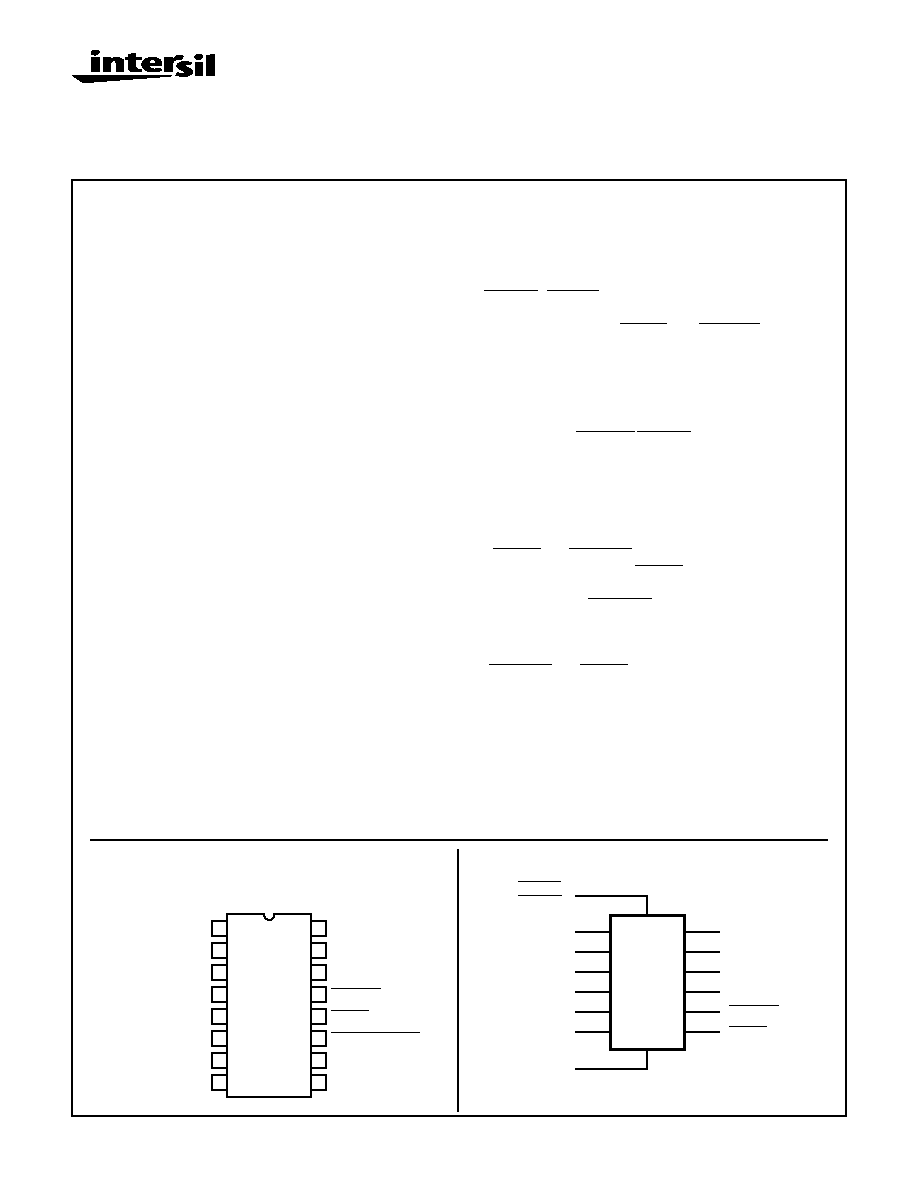
CMOS Presettable Up/Down Counters
(Dual Clock With Reset)
Description
CD40192BMS Presettable BCD Up/Down Counter and the
CD40193BMS Presettable Binary Up/Down Counter each con-
sist of 4 synchronously clocked, gated "D" type flip-flops con-
nected as a counter. The inputs consist of 4 individual jam lines,
a PRESET ENABLE control, individual CLOCK UP and
CLOCK DOWN signals and a master RESET. Four buffered Q
signal outputs as well as CARRY and BORROW outputs for
multiple-stage counting schemes are provided.
The counter is cleared so that all outputs are in a low state by a
high on the RESET line. A RESET is accomplished asynchro-
nously with the clock. Each output is individually programmable
asynchronously with the clock to the level on the corresponding
jam input when the PRESET ENABLE control is low.
The counter counts up one count on the positive clock edge of
the CLOCK UP signal provided the CLOCK DOWN line is high.
The counter counts down one count on the positive clock edge
of the CLOCK DOWN signal provided the CLOCK UP line is
high.
The CARRY and BORROW signals are high when the counter
is counting up or down. The CARRY signal goes low one-half
clock cycle after the counter reaches its maximum count in the
count-up mode. The BORROW signal goes low one-half clock
cycle after the counter reaches its minimum count in the count-
down mode. Cascading of multiple packages is easily accom-
plished without the need for additional external circuitry by tying
the BORROW and CARRY outputs to the CLOCK DOWN and
CLOCK UP inputs, respectively, of the succeeding counter
package.
The CD40192BMS and CD40193BMS are supplied in these
16-lead outline packages:
Braze Seal DIP
*H4W,
H4X
Frit Seal DIP
H1F
Ceramic Flatpack
*H6P,
H6W
* CD40192B Only
CD40193B Only
Features
∑ CD40192BMS - BCD Type
∑ CD40193BMS - Binary Type
∑ High Voltage Type (20V Rating)
∑ Individual Clock Lines for Counting Up or Counting
Down
∑ Synchronous High-Speed Carry and Borrow Propaga-
tion Delays for Cascading
∑ Asynchronous Reset and Preset Capability
∑ Medium Speed Operation
- fCL = 8MHz (typ.) at 10V
∑ 5V, 10V and 15V Parametric Ratings
∑ Standardize Symmetrical Output Characteristics
∑ 100% Tested for Quiescent Current at 20V
∑ Maximum Input Current of 1
µ
A at 18V Over Full Pack-
age Temperature Range; 100nA at 18V and +25
o
C
∑ Noise Margin (Over Full Package/Temperature Range)
- 1V at VDD = 5V
- 2V at VDD = 10V
- 2.5V at VDD = 15V
∑ Meets All Requirements of JEDEC Tentative Standard
No. 13B, "Standard Specifications for Description of
`B' Series CMOS Devices"
Applications
∑ Up/Down Difference Counting
∑ Multistage Ripple Counting
∑ Synchronous Frequency Dividers
∑ A/D and D/A Conversion
∑ Programmable Binary or BCD Counting
File Number
3363
December 1992
Pinout
CD40192BMS, CD40193BMS
TOP VIEW
14
15
16
9
13
12
11
10
1
2
3
4
5
7
6
8
J2
Q2
Q1
CLOCK UP
Q3
VSS
Q4
VDD
RESET
BORROW
CARRY
PRESET ENABLE
J3
J4
J1
CLOCK DOWN
Functional Diagram
3
2
6
7
12
Q1
Q2
Q3
Q4
BORROW
CARRY
15
1
10
9
5
J1
J2
J3
J4
CLOCK UP
CLOCK DOWN
11
14
PRESET
ENABLE
RESET
VDD = 16
VSS = 8
13
4
7-1420
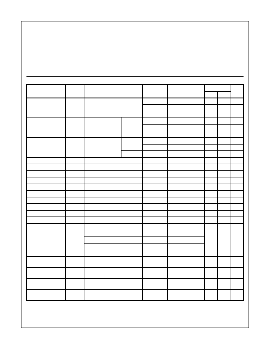
Specifications CD40192BMS, CD40193BMS
Absolute Maximum Ratings
Reliability Information
DC Supply Voltage Range, (VDD) . . . . . . . . . . . . . . . -0.5V to +20V
(Voltage Referenced to VSS Terminals)
Input Voltage Range, All Inputs . . . . . . . . . . . . .-0.5V to VDD +0.5V
DC Input Current, Any One Input
. . . . . . . . . . . . . . . . . . . . . . . .±
10mA
Operating Temperature Range . . . . . . . . . . . . . . . . -55
o
C to +125
o
C
Package Types D, F, K, H
Storage Temperature Range (TSTG) . . . . . . . . . . . -65
o
C to +150
o
C
Lead Temperature (During Soldering) . . . . . . . . . . . . . . . . . +265
o
C
At Distance 1/16
±
1/32 Inch (1.59mm
±
0.79mm) from case for
10s Maximum
Thermal Resistance
ja
jc
Ceramic DIP and FRIT Package . . . . .
80
o
C/W
20
o
C/W
Flatpack Package . . . . . . . . . . . . . . . .
70
o
C/W
20
o
C/W
Maximum Package Power Dissipation (PD) at +125
o
C
For T
A
= -55
o
C to +100
o
C (Package Type D, F, K) . . . . . . 500mW
For T
A
= +100
o
C to +125
o
C (Package Type D, F, K). . . . . . Derate
Linearity at 12mW/
o
C to 200mW
Device Dissipation per Output Transistor . . . . . . . . . . . . . . . 100mW
For T
A
= Full Package Temperature Range (All Package Types)
Junction Temperature . . . . . . . . . . . . . . . . . . . . . . . . . . . . . . +175
o
C
TABLE 1. DC ELECTRICAL PERFORMANCE CHARACTERISTICS
PARAMETER
SYMBOL
CONDITIONS (NOTE 1)
GROUP A
SUBGROUPS
TEMPERATURE
LIMITS
UNITS
MIN
MAX
Supply Current
IDD
VDD = 20V, VIN = VDD or GND
1
+25
o
C
-
10
µ
A
2
+125
o
C
-
1000
µ
A
VDD = 18V, VIN = VDD or GND
3
-55
o
C
-
10
µ
A
Input Leakage Current
IIL
VIN = VDD or GND
VDD = 20V
1
+25
o
C
-100
-
nA
2
+125
o
C
-1000
-
nA
VDD = 18V
3
-55
o
C
-100
-
nA
Input Leakage Current
IIH
VIN = VDD or GND
VDD = 20V
1
+25
o
C
-
100
nA
2
+125
o
C
-
1000
nA
VDD = 18V
3
-55
o
C
-
100
nA
Output Voltage
VOL15
VDD = 15V, No Load
1, 2, 3
+25
o
C, +125
o
C, -55
o
C
-
50
mV
Output Voltage
VOH15
VDD = 15V, No Load (Note 3)
1, 2, 3
+25
o
C, +125
o
C, -55
o
C 14.95
-
V
Output Current (Sink)
IOL5
VDD = 5V, VOUT = 0.4V
1
+25
o
C
0.53
-
mA
Output Current (Sink)
IOL10
VDD = 10V, VOUT = 0.5V
1
+25
o
C
1.4
-
mA
Output Current (Sink)
IOL15
VDD = 15V, VOUT = 1.5V
1
+25
o
C
3.5
-
mA
Output Current (Source)
IOH5A
VDD = 5V, VOUT = 4.6V
1
+25
o
C
-
-0.53
mA
Output Current (Source)
IOH5B
VDD = 5V, VOUT = 2.5V
1
+25
o
C
-
-1.8
mA
Output Current (Source)
IOH10
VDD = 10V, VOUT = 9.5V
1
+25
o
C
-
-1.4
mA
Output Current (Source)
IOH15
VDD = 15V, VOUT = 13.5V
1
+25
o
C
-
-3.5
mA
N Threshold Voltage
VNTH
VDD = 10V, ISS = -10
µ
A
1
+25
o
C
-2.8
-0.7
V
P Threshold Voltage
VPTH
VSS = 0V, IDD = 10
µ
A
1
+25
o
C
0.7
2.8
V
Functional
F
VDD = 2.8V, VIN = VDD or GND
7
+25
o
C
VOH >
VDD/2
VOL <
VDD/2
V
VDD = 20V, VIN = VDD or GND
7
+25
o
C
VDD = 18V, VIN = VDD or GND
8A
+125
o
C
VDD = 3V, VIN = VDD or GND
8B
-55
o
C
Input Voltage Low
(Note 2)
VIL
VDD = 5V, VOH > 4.5V, VOL < 0.5V
1, 2, 3
+25
o
C, +125
o
C, -55
o
C
-
1.5
V
Input Voltage High
(Note 2)
VIH
VDD = 5V, VOH > 4.5V, VOL < 0.5V
1, 2, 3
+25
o
C, +125
o
C, -55
o
C
3.5
-
V
Input Voltage Low
(Note 2)
VIL
VDD = 15V, VOH > 13.5V,
VOL < 1.5V
1, 2, 3
+25
o
C, +125
o
C, -55
o
C
-
4
V
Input Voltage High
(Note 2)
VIH
VDD = 15V, VOH > 13.5V,
VOL < 1.5V
1, 2, 3
+25
o
C, +125
o
C, -55
o
C
11
-
V
NOTES: 1. All voltages referenced to device GND, 100% testing being
implemented.
2. Go/No Go test with limits applied to inputs.
3. For accuracy, voltage is measured differentially to VDD. Limit
is 0.050V max.
7-1421
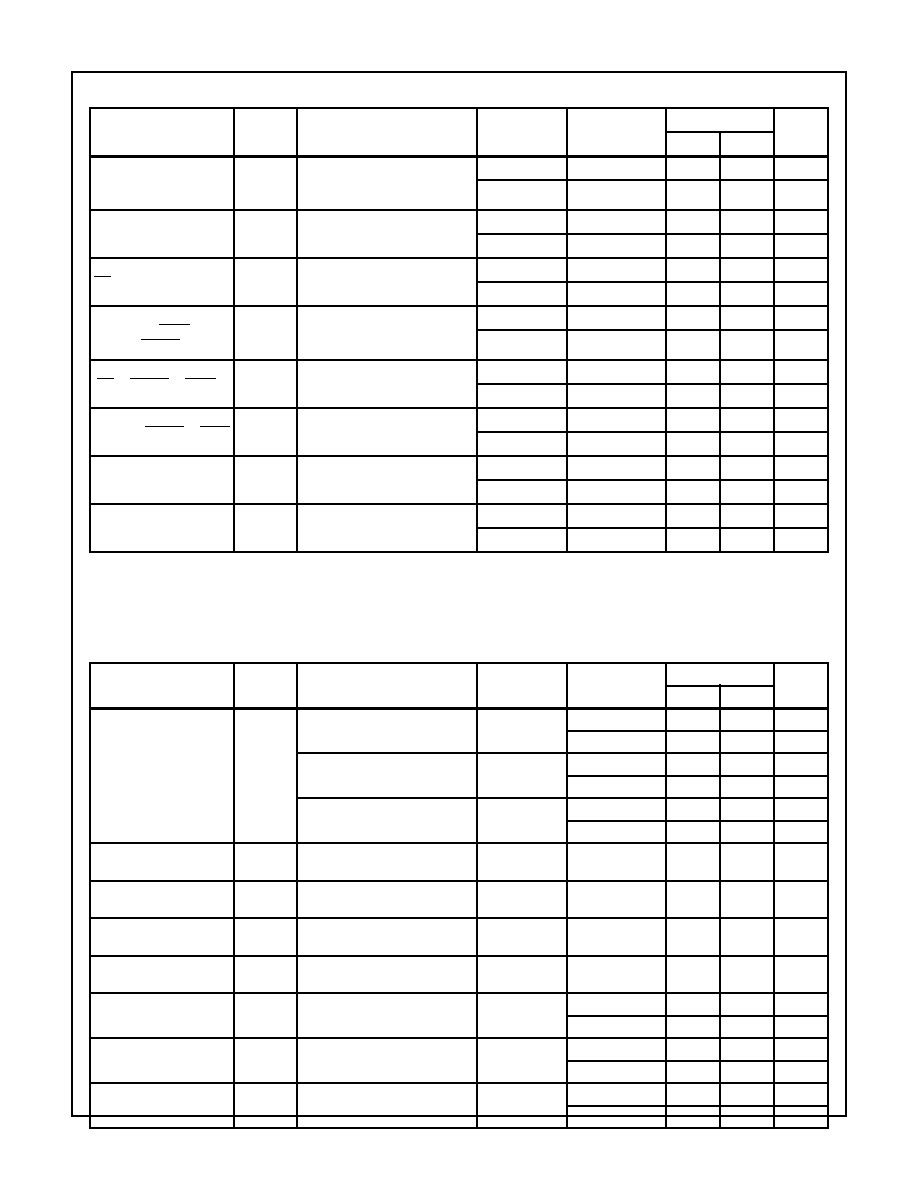
Specifications CD40192BMS, CD40193BMS
TABLE 2. AC ELECTRICAL PERFORMANCE CHARACTERISTICS
PARAMETER
SYMBOL
CONDITIONS (NOTES 1, 2)
GROUP A
SUBGROUPS
TEMPERATURE
LIMITS
UNITS
MIN
MAX
Propagation Delay
Clock Up or Clock Down
to Q
TPHL1
TPLH1
VDD = 5V, VIN = VDD or GND
9
+25
o
C
-
500
ns
10, 11
+125
o
C, -55
o
C
-
675
ns
Propagation Delay
Reset to Q
TPHL2
VDD = 5V, VIN = VDD or GND
9
+25
o
C
-
500
ns
10, 11
+125
o
C, -55
o
C
-
675
ns
Propagation Delay
PE to Q
TPHL3
TPLH3
VDD = 5V, VIN = VDD or GND
9
+25
o
C
-
400
ns
10, 11
+125
o
C, -55
o
C
-
540
ns
Propagation Delay
Clock Up to Carry, Clock
Down to Borrow
TPHL4
TPLH4
VDD = 5V, VIN = VDD or GND
9
+25
o
C
-
320
ns
10, 11
+125
o
C, -55
o
C
-
432
ns
Propagation Delay
PE to Borrow or Carry
TPHL5
TPLH5
VDD = 5V, VIN = VDD or GND
9
+25
o
C
-
600
ns
10, 11
+125
o
C, -55
o
C
-
810
ns
Propagation Delay
Reset to Borrow or Carry
TPHL6
TPLH6
VDD = 5V, VIN = VDD or GND
9
+25
o
C
-
600
ns
10, 11
+125
o
C, -55
o
C
-
810
ns
Transition Time
TTHL
TTLH
VDD = 5V, VIN = VDD or GND
9
+25
o
C
-
200
ns
10, 11
+125
o
C, -55
o
C
-
270
ns
Maximum Clock Input
Frequency
FCL
VDD = 5V, VIN = VDD or GND
9
+25
o
C
2
-
MHz
10, 11
+125
o
C, -55
o
C
1.48
-
MHz
NOTES:
1. CL = 50pF, RL = 200K, Input TR, TF < 20ns.
2. -55
o
C and +125
o
C limits guaranteed, 100% testing being implemented.
TABLE 3. ELECTRICAL PERFORMANCE CHARACTERISTICS
PARAMETER
SYMBOL
CONDITIONS
NOTES
TEMPERATURE
LIMITS
UNITS
MIN
MAX
Supply Current
IDD
VDD = 5V, VIN = VDD or GND
1, 2
-55
o
C, +25
o
C
-
5
µ
A
+125
o
C
-
150
µ
A
VDD = 10V, VIN = VDD or GND
1, 2
-55
o
C, +25
o
C
-
10
µ
A
+125
o
C
-
300
µ
A
VDD = 15V, VIN = VDD or GND
1, 2
-55
o
C, +25
o
C
-
10
µ
A
+125
o
C
-
600
µ
A
Output Voltage
VOL
VDD = 5V, No Load
1, 2
+25
o
C, +125
o
C,
-55
o
C
-
50
mV
Output Voltage
VOL
VDD = 10V, No Load
1, 2
+25
o
C, +125
o
C,
-55
o
C
-
50
mV
Output Voltage
VOH
VDD = 5V, No Load
1, 2
+25
o
C, +125
o
C,
-55
o
C
4.95
-
V
Output Voltage
VOH
VDD = 10V, No Load
1, 2
+25
o
C, +125
o
C,
-55
o
C
9.95
-
V
Output Current (Sink)
IOL5
VDD = 5V, VOUT = 0.4V
1, 2
+125
o
C
0.36
-
mA
-55
o
C
0.64
-
mA
Output Current (Sink)
IOL10
VDD = 10V, VOUT = 0.5V
1, 2
+125
o
C
0.9
-
mA
-55
o
C
1.6
-
mA
Output Current (Sink)
IOL15
VDD = 15V, VOUT = 1.5V
1, 2
+125
o
C
2.4
-
mA
-55
o
C
4.2
-
mA
7-1422
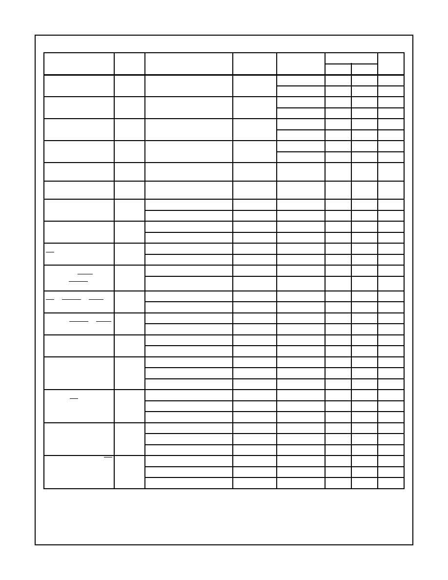
Specifications CD40192BMS, CD40193BMS
Output Current (Source)
IOH5A
VDD = 5V, VOUT = 4.6V
1, 2
+125
o
C
-
-0.36
mA
-55
o
C
-
-0.64
mA
Output Current (Source)
IOH5B
VDD = 5V, VOUT = 2.5V
1, 2
+125
o
C
-
-1.15
mA
-55
o
C
-
-2.0
mA
Output Current (Source)
IOH10
VDD = 10V, VOUT = 9.5V
1, 2
+125
o
C
-
-0.9
mA
-55
o
C
-
-1.6
mA
Output Current (Source)
IOH15
VDD =15V, VOUT = 13.5V
1, 2
+125
o
C
-
-2.4
mA
-55
o
C
-
-4.2
mA
Input Voltage Low
VIL
VDD = 10V, VOH > 9V, VOL < 1V
1, 2
+25
o
C, +125
o
C,
-55
o
C
-
3
V
Input Voltage High
VIH
VDD = 10V, VOH > 9V, VOL < 1V
1, 2
+25
o
C, +125
o
C,
-55
o
C
7
-
V
Propagation Delay
Clock Up or Down to Q
TPHL1
TPLH1
VDD = 10V
1, 2, 3
+25
o
C
-
240
ns
VDD = 15V
1, 2, 3
+25
o
C
-
180
ns
Propagation Delay
Reset to Q
TPHL2
VDD = 10V
1, 2, 3
+25
o
C
-
240
ns
VDD = 15V
1, 2, 3
+25
o
C
-
180
ns
Propagation Delay
PE to Q
TPHL3
TPLH3
VDD = 10V
1, 2, 3
+25
o
C
-
200
ns
VDD = 15V
1, 2, 3
+25
o
C
-
140
ns
Propagation Delay
Clock Up to Carry, Clock
Down to Borrow
TPHL4
TPLH4
VDD = 10V
1, 2, 3
+25
o
C
-
160
ns
VDD = 15V
1, 2, 3
+25
o
C
-
120
ns
Propagation Delay
PE to Borrow or Carry
TPHL5
TPLH5
VDD = 10V
1, 2, 3
+25
o
C
-
300
ns
VDD = 15V
1, 2, 3
+25
o
C
-
220
ns
Propagation Delay
Reset to Borrow or Carry
TPHL6
TPLH6
VDD = 10V
1, 2, 3
+25
o
C
-
300
ns
VDD = 15V
1, 2, 3
+25
o
C
-
220
ns
Transition Time
TTHL1
TTLH1
VDD = 10V
1, 2, 3
+25
o
C
-
100
ns
VDD = 15V
1, 2, 3
+25
o
C
-
80
ns
Maximum Clock Rise and
Fall Time
TRCL
TFCL
VDD = 5V
1, 2, 3, 4
+25
o
C
-
15
µ
s
VDD = 10V
1, 2, 3, 4
+25
o
C
-
15
µ
s
VDD = 15V
1, 2, 3, 4
+25
o
C
-
5
µ
s
Minimum Removal Time
Reset or PE
TREM
VDD = 5V
1, 2, 3, 5
+25
o
C
-
80
ns
VDD = 10V
1, 2, 3, 5
+25
o
C
-
40
ns
VDD = 15V
1, 2, 3, 5
+25
o
C
-
30
ns
Minimum Pulse Width
Reset
TW
VDD = 5V
1, 2, 3
+25
o
C
-
480
ns
VDD = 10V
1, 2, 3
+25
o
C
-
300
ns
VDD = 15V
1, 2, 3
+25
o
C
-
260
ns
Minimum Pulse Width PE
TW
VDD = 5V
1, 2, 3
+25
o
C
-
240
ns
VDD = 10V
1, 2, 3
+25
o
C
-
170
ns
VDD = 15V
1, 2, 3
+25
o
C
-
140
ns
TABLE 3. ELECTRICAL PERFORMANCE CHARACTERISTICS (Continued)
PARAMETER
SYMBOL
CONDITIONS
NOTES
TEMPERATURE
LIMITS
UNITS
MIN
MAX
7-1423
Specifications CD40192BMS, CD40193BMS
Minimum Clock Pulse
Width
TW
VDD = 5V
1, 2, 3
+25
o
C
-
180
ns
VDD = 10V
1, 2, 3
+25
o
C
-
90
ns
VDD = 15V
1, 2, 3
+25
o
C
-
60
ns
Input Capacitance
CIN
Reset
1, 2
+25
o
C
-
15
pF
Input Capacitance
CIN
All Other Inputs
1, 2
+25
o
C
-
7.5
pF
NOTES:
1. All voltages referenced to device GND.
2. The parameters listed on Table 3 are controlled via design or process and are not directly tested. These parameters are characterized on
initial design release and upon design changes which would affect these characteristics.
3. CL = 50pF, RL = 200K, Input TR, TF < 20ns.
4. If more than one unit is cascaded, TRCL should be made less than or equal to the sumof the transition time and the fixed propagation
delay of the output of the driving stage for the estimated capacitive load.
5. The time required for RESET or PRESET ENABLE control to be removed before clocking. See timing diagram defining TREM.
TABLE 4. POST IRRADIATION ELECTRICAL PERFORMANCE CHARACTERISTICS
PARAMETER
SYMBOL
CONDITIONS
NOTES
TEMPERATURE
LIMITS
UNITS
MIN
MAX
Supply Current
IDD
VDD = 20V, VIN = VDD or GND
1, 4
+25
o
C
-
25
µ
A
N Threshold Voltage
VNTH
VDD = 10V, ISS = -10
µ
A
1, 4
+25
o
C
-2.8
-0.2
V
N Threshold Voltage
Delta
VTN
VDD = 10V, ISS = -10
µ
A
1, 4
+25
o
C
-
±
1
V
P Threshold Voltage
VTP
VSS = 0V, IDD = 10
µ
A
1, 4
+25
o
C
0.2
2.8
V
P Threshold Voltage
Delta
VTP
VSS = 0V, IDD = 10
µ
A
1, 4
+25
o
C
-
±
1
V
Functional
F
VDD = 18V, VIN = VDD or GND
1
+25
o
C
VOH >
VDD/2
VOL <
VDD/2
V
VDD = 3V, VIN = VDD or GND
Propagation Delay Time
TPHL
TPLH
VDD = 5V
1, 2, 3, 4
+25
o
C
-
1.35 x
+25
o
C
Limit
ns
NOTES: 1. All voltages referenced to device GND.
2. CL = 50pF, RL = 200K, Input TR, TF < 20ns.
3. See Table 2 for +25
o
C limit.
4. Read and Record
TABLE 5. BURN-IN AND LIFE TEST DELTA PARAMETERS +25
o
C
PARAMETER
SYMBOL
DELTA LIMIT
Supply Current - MSI-2
IDD
±
1.0
µ
A
Output Current (Sink)
IOL5
±
20% x Pre-Test Reading
Output Current (Source)
IOH5A
±
20% x Pre-Test Reading
TABLE 3. ELECTRICAL PERFORMANCE CHARACTERISTICS (Continued)
PARAMETER
SYMBOL
CONDITIONS
NOTES
TEMPERATURE
LIMITS
UNITS
MIN
MAX