7-1431
CAUTION: These devices are sensitive to electrostatic discharge; follow proper IC Handling Procedures.
1-888-INTERSIL or 321-724-7143 | Copyright © Intersil Corporation 1999
CD40208BMS
CMOS 4 x 4 Multiport Register
Description
The CD40208BMS is a 4 x 4 multiport register containing
four 4-bit registers, write address decoder, two separate
read address decoders, and two 3-state output buses.
When the ENABLE input is low, the corresponding output
bus is switched, independently of the clock, to a high imped-
ance state. The high impedance third state provides the out-
puts with the capability of being connected to the bus lines in
a bus organized system without the need for interface or
pull-up components.
When the WRITE ENABLE input is high, all data input lines
are latched on the positive transition of the CLOCK and the
data is entered into the word selected by the write address
lines. When WRITE ENABLE is low, the CLOCK is inhibited
and no new data is entered. In either case, the contents of
any word may be accessed via the read address lines inde-
pendent of the state of the CLOCK input.
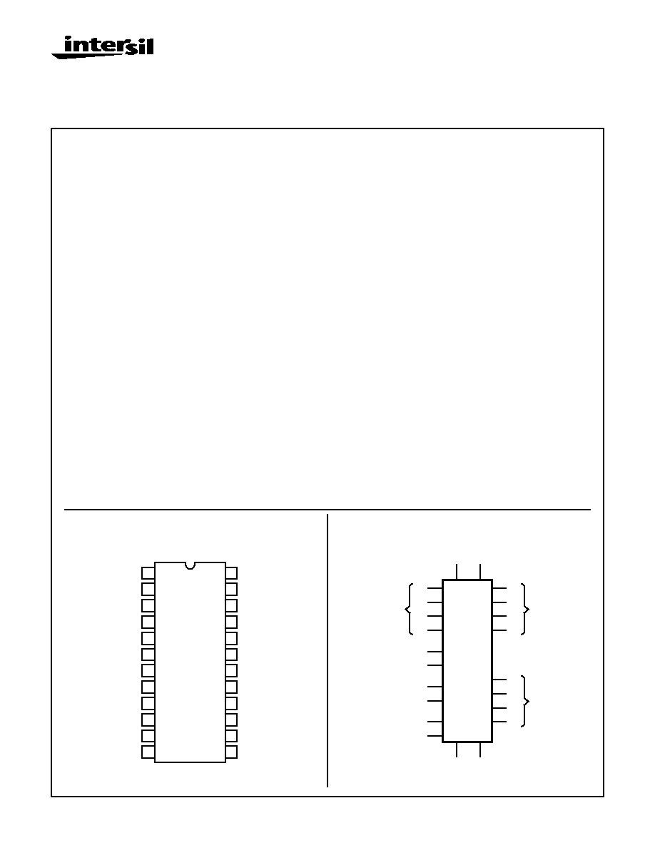
The CD40208BMS types are supplied in hermetic 24-lead
dual-in-line ceramic packages (D and F suffixes), 24-lead
dual-in-line plastic packages (E suffix), 24-lead ceramic flat
packages (K suffix), and in chip form (H suffix).
The CD40208BMS is supplied in these 24-lead outline pack-
ages:
Braze Seal DIP
HNZ
Ceramic Flatpack
H4P
Features
∑ High Voltage Types (20V Rating)
∑ One Input and Two Output Buses
∑ Unlimited Expansion in Bit and Word Directions
∑ Data Lines have Latched Inputs
∑ 3-State Outputs
∑ Separate Control of Each Bus, Allowing Simultaneous
Independent Reading of any of Four Registers on Bus
A and Bus B and Independent Writing Into any of the
Four Registers
∑ 100% Tested for Quiescent Current at 20V
∑ Standardized, Symmetrical Output Characteristics
∑ 5V, 10V and 15V Parametric Ratings
∑ Maximum Input Current of 1
µ
A at 18V Over Full Pack-
age-Temperature Range; 100nA at 18V and +25
o
C
∑ Noise Margin (Full Package-Temperature Range):
- 1V at VDD = 5V
- 2V at VDD = 10V
- 2.5V at VDD = 15V
∑ Meets All Requirements of JEDEC Tentative Stan-
dards No. 13B, "Standard Specifications for Descrip-
tion of "B" Series CMOS Devices"
Applications
∑ Scratch Pad Memories
∑ Arithmetic Units
∑ Data Storage
December 1992
File Number
3396
Pinout
CD40208BMS
TOP VIEW
1
2
3
4
5
6
7
8
9
10
11
12
Q3B
Q2B
ENABLE A
Q0A
Q1A
Q2A
Q3A
WRITE 0
WRITE 1
READ 0B
READ 1B
VSS
16
17
18
19
20
21
22
23
24
15
14
13
VDD
Q0B
ENABLE B
D0
D1
D3
WRITE ENABLE
READ 1A
READ 0A
Q1B
D2
CLOCK
Functional Diagram
WRITE
ENABLE
ENABLE A
3
15
20
19
18
17
8
9
14
13
11
10
4
5
6
7
22
23
2
1
Q0
Q1
Q2
Q3
Q0
Q1
Q2
Q3
READ 1A
READ 0A
READ 1B
READ 0B
16
21
WRITE 1
WRITE 0
D0
D1
D2
D3
DATA
INPUTS
WORD A
OUTPUT
WORD B
OUTPUT
CLOCK
ENABLE B
V
DD
= 24
V
SS
= 12
7-1432
Specifications CD40208BMS
Absolute Maximum Ratings
Reliability Information
DC Supply Voltage Range, (VDD) . . . . . . . . . . . . . . . -0.5V to +20V
(Voltage Referenced to VSS Terminals)
Input Voltage Range, All Inputs . . . . . . . . . . . . .-0.5V to VDD +0.5V
DC Input Current, Any One Input
. . . . . . . . . . . . . . . . . . . . . . . .±
10mA
Operating Temperature Range . . . . . . . . . . . . . . . . -55
o
C to +125
o
C
Package Types D, F, K, H
Storage Temperature Range (TSTG) . . . . . . . . . . . -65
o
C to +150
o
C
Lead Temperature (During Soldering) . . . . . . . . . . . . . . . . . +265
o
C
At Distance 1/16
±
1/32 Inch (1.59mm
±
0.79mm) from case for
10s Maximum
Thermal Resistance
ja
jc
Ceramic DIP and Frit Package . . . . . .
80
o
C/W
20
o
C/W
Flatpack Package . . . . . . . . . . . . . . . .
70
o
C/W
20
o
C/W
Maximum Package Power Dissipation (PD) at +125
o
C
For T
A
= -55
o
C to +100
o
C (Package Type D, F, K) . . . . . . 500mW
For T
A
= +100
o
C to +125
o
C (Package Type D, F, K). . . . . . Derate
Linearity at 12mW/
o
C to 200mW
Device Dissipation per Output Transistor . . . . . . . . . . . . . . . 100mW
For T
A
= Full Package Temperature Range (All Package Types)
Junction Temperature . . . . . . . . . . . . . . . . . . . . . . . . . . . . . . +175
o
C
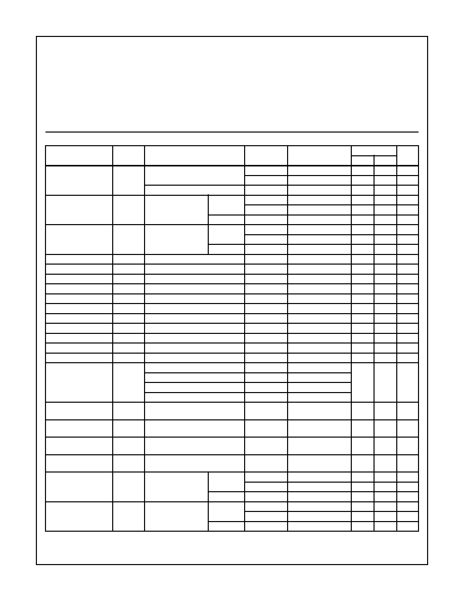
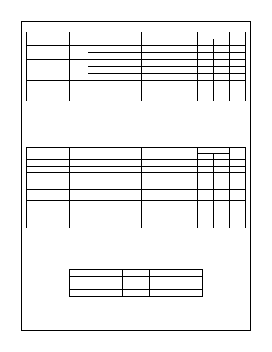
TABLE 1. DC ELECTRICAL PERFORMANCE CHARACTERISTICS
PARAMETER
SYMBOL
CONDITIONS (NOTE 1)
GROUP A
SUBGROUPS
TEMPERATURE
LIMITS
UNITS
MIN
MAX
Supply Current
IDD
VDD = 20V, VIN = VDD or GND
1
+25
o
C
-
10
µ
A
2
+125
o
C
-
1000
µ
A
VDD = 18V, VIN = VDD or GND
3
-55
o
C
-
10
µ
A
Input Leakage Current
IIL
VIN = VDD or GND
VDD = 20
1
+25
o
C
-100
-
nA
2
+125
o
C
-1000
-
nA
VDD = 18V
3
-55
o
C
-100
-
nA
Input Leakage Current
IIH
VIN = VDD or GND
VDD = 20
1
+25
o
C
-
100
nA
2
+125
o
C
-
1000
nA
VDD = 18V
3
-55
o
C
-
100
nA
Output Voltage
VOL15
VDD = 15V, No Load
1, 2, 3
+25
o
C, +125
o
C, -55
o
C
-
50
mV
Output Voltage
VOH15
VDD = 15V, No Load (Note 3)
1, 2, 3
+25
o
C, +125
o
C, -55
o
C 14.95
-
V
Output Current (Sink)
IOL5
VDD = 5V, VOUT = 0.4V
1
+25
o
C
0.53
-
mA
Output Current (Sink)
IOL10
VDD = 10V, VOUT = 0.5V
1
+25
o
C
1.4
-
mA
Output Current (Sink)
IOL15
VDD = 15V, VOUT = 1.5V
1
+25
o
C
3.5
-
mA
Output Current (Source)
IOH5A
VDD = 5V, VOUT = 4.6V
1
+25
o
C
-
-0.53
mA
Output Current (Source)
IOH5B
VDD = 5V, VOUT = 2.5V
1
+25
o
C
-
-1.8
mA
Output Current (Source)
IOH10
VDD = 10V, VOUT = 9.5V
1
+25
o
C
-
-1.4
mA
Output Current (Source)
IOH15
VDD = 15V, VOUT = 13.5V
1
+25
o
C
-
-3.5
mA
N Threshold Voltage
VNTH
VDD = 10V, ISS = -10
µ
A
1
+25
o
C
-2.8
-0.7
V
P Threshold Voltage
VPTH
VSS = 0V, IDD = 10
µ
A
1
+25
o
C
0.7
2.8
V
Functional
F
VDD = 2.8V, VIN = VDD or GND
7
+25
o
C
VOH >
VDD/2
VOL <
VDD/2
V
VDD = 20V, VIN = VDD or GND
7
+25
o
C
VDD = 18V, VIN = VDD or GND
8A
+125
o
C
VDD = 3V, VIN = VDD or GND
8B
-55
o
C
Input Voltage Low
(Note 2)
VIL
VDD = 5V, VOH > 4.5V, VOL < 0.5V
1, 2, 3
+25
o
C, +125
o
C, -55
o
C
-
1.5
V
Input Voltage High
(Note 2)
VIH
VDD = 5V, VOH > 4.5V, VOL < 0.5V
1, 2, 3
+25
o
C, +125
o
C, -55
o
C
3.5
-
V
Input Voltage Low
(Note 2)
VIL
VDD = 15V, VOH > 13.5V,
VOL < 1.5V
1, 2, 3
+25
o
C, +125
o
C, -55
o
C
-
4
V
Input Voltage High
(Note 2)
VIH
VDD = 15V, VOH > 13.5V,
VOL < 1.5V
1, 2, 3
+25
o
C, +125
o
C, -55
o
C
11
-
V
Tri-State Output
Leakage
IOZL
VIN = VDD or GND
VOUT = 0V
VDD = 20V
1
+25
o
C
-0.4
-
µ
A
2
+125
o
C
-12
-
µ
A
VDD = 18V
3
-55
o
C
-0.4
-
µ
A
Tri-State Output
Leakage
IOZH
VIN = VDD or GND
VOUT = VDD
VDD = 20V
1
+25
o
C
-
0.4
µ
A
2
+125
o
C
-
12
µ
A
VDD = 18V
3
-55
o
C
-
0.4
µ
A
NOTES: 1. All voltages referenced to device GND, 100% testing being
implemented.
2. Go/NoGo test with limits applied to inputs.
3. For accuracy, voltage is measured differentially to VDD. Limit
is 0.050V max.
7-1433
Specifications CD40208BMS
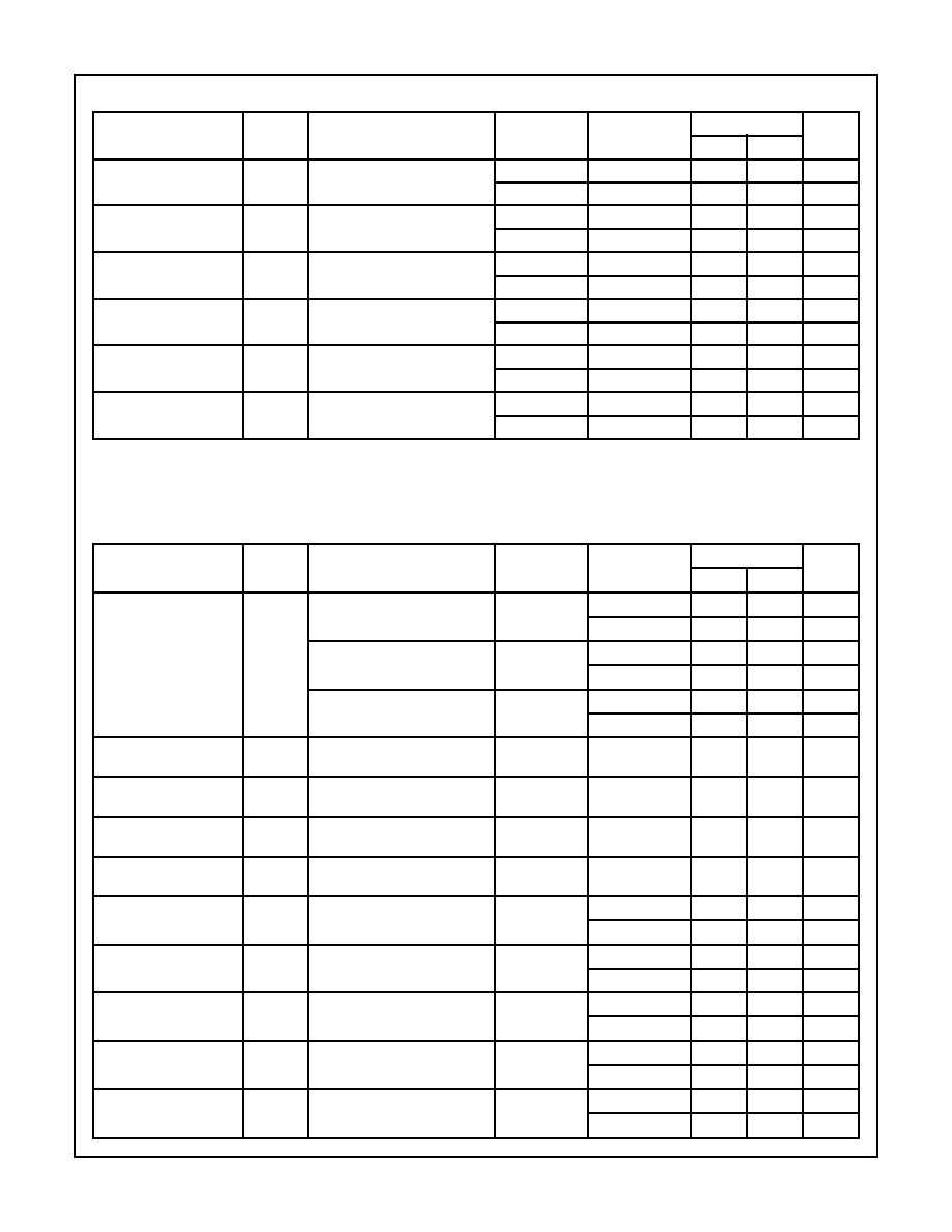
TABLE 2. AC ELECTRICAL PERFORMANCE CHARACTERISTICS
PARAMETER
SYMBOL
CONDITIONS (NOTE 1)
GROUP A
SUBGROUPS
TEMPERATURE
LIMITS
UNITS
MIN
MAX
Propagation Delay
Clock or Write Enable to Q
TPHL1
TPLH1
VDD = 5V, VIN = VDD or GND
(Notes 1, 2)
9
+25
o
C
-
720
ns
10, 11
+125
o
C, -55
o
C
-
972
ns
Propagation Delay
Read or Write Enable to Q
TPHL2
TPLH2
VDD = 5V, VIN = VDD or GND
(Notes 1, 2)
9
+25
o
C
-
600
ns
10, 11
+125
o
C, -55
o
C
-
810
ns
Propagation Delay
3-State Disable Delay Time
TPZH, HZ VDD = 5V, VIN = VDD or GND
(Notes 2, 3)
9
+25
o
C
-
200
ns
10, 11
+125
o
C, -55
o
C
-
270
ns
Propagation Delay
3-State Disable Delay Time
TPZL, LZ VDD = 5V, VIN = VDD or GND
(Notes 2, 3)
9
+25
o
C
-
260
ns
10, 11
+125
o
C, -55
o
C
-
351
ns
Transition Time
TTHL
TTLH
VDD = 5V, VIN = VDD or GND
(Notes 1, 2)
9
+25
o
C
-
200
ns
10, 11
+125
o
C, -55
o
C
-
270
ns
Maximum Clock Input
Frequency
FCL
VDD = 5V, VIN = VDD or GND
9
+25
o
C
1.5
-
MHz
10, 11
+125
o
C, -55
o
C
1.11
-
MHz
NOTES:
1. VDD = 5V, CL = 50pF, RL = 200K
2. -55
o
C and +125
o
C limits guaranteed, 100% testing being implemented.
TABLE 3. ELECTRICAL PERFORMANCE CHARACTERISTICS
PARAMETER
SYMBOL
CONDITIONS
NOTES
TEMPERATURE
LIMITS
UNITS
MIN
MAX
Supply Current
IDD
VDD = 5V, VIN = VDD or GND
1, 2
-55
o
C, +25
o
C
-
5
µ
A
+125
o
C
-
150
µ
A
VDD = 10V, VIN = VDD or GND
1, 2
-55
o
C, +25
o
C
-
10
µ
A
+125
o
C
-
300
µ
A
VDD = 15V, VIN = VDD or GND
1, 2
-55
o
C, +25
o
C
-
10
µ
A
+125
o
C
-
600
µ
A
Output Voltage
VOL
VDD = 5V, No Load
1, 2
+25
o
C, +125
o
C,
-55
o
C
-
50
mV
Output Voltage
VOL
VDD = 10V, No Load
1, 2
+25
o
C, +125
o
C,
-55
o
C
-
50
mV
Output Voltage
VOH
VDD = 5V, No Load
1, 2
+25
o
C, +125
o
C,
-55
o
C
4.95
-
V
Output Voltage
VOH
VDD = 10V, No Load
1, 2
+25
o
C, +125
o
C,
-55
o
C
9.95
-
V
Output Current (Sink)
IOL4
VDD = 4.5V, VOUT = 0.4V
1, 2
+125
o
C
-
-
mA
-55
o
C
-
-
mA
Output Current (Sink)
IOL5
VDD = 5V, VOUT = 0.4V
1, 2
+125
o
C
0.36
-
mA
-55
o
C
0.64
-
mA
Output Current (Sink)
IOL10
VDD = 10V, VOUT = 0.5V
1, 2
+125
o
C
0.9
-
mA
-55
o
C
1.6
-
mA
Output Current (Sink)
IOL15
VDD = 15V, VOUT = 1.5V
1, 2
+125
o
C
2.4
-
mA
-55
o
C
4.2
-
mA
Output Current (Source)
IOH5A
VDD = 5V, VOUT = 4.6V
1, 2
+125
o
C
-
-0.36
mA
-55
o
C
-
-0.64
mA
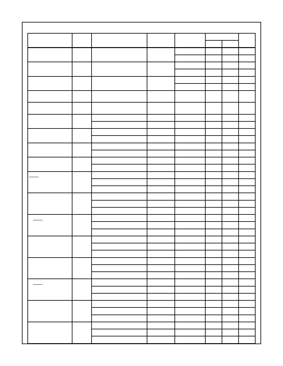
7-1434
Specifications CD40208BMS
Output Current (Source)
IOH5B
VDD = 5V, VOUT = 2.5V
1, 2
+125
o
C
-
-1.15
mA
-55
o
C
-
-2.0
mA
Output Current (Source)
IOH10
VDD = 10V, VOUT = 9.5V
1, 2
+125
o
C
-
-0.9
mA
-55
o
C
-
-1.6
mA
Output Current (Source)
IOH15
VDD =15V, VOUT = 13.5V
1, 2
+125
o
C
-
-2.4
mA
-55
o
C
-
-4.2
mA
Input Voltage Low
VIL
VDD = 10V, VOH > 9V, VOL < 1V
1, 2
+25
o
C, +125
o
C,
-55
o
C
-
3
V
Input Voltage High
VIH
VDD = 10V, VOH > 9V, VOL < 1V
1, 2
+25
o
C, +125
o
C,
-55
o
C
+7
-
V
Propagation Delay
Clock or Write Enable to Q
TPHL1
TPLH1
VDD = 10V
1, 2, 3
+25
o
C
-
280
ns
VDD = 15V
1, 2, 3
+25
o
C
-
200
ns
Propagation Delay
Read or Write Address to Q
TPHL2
TPLH2
VDD = 10V
1, 2, 3
+25
o
C
-
240
ns
VDD = 15V
1, 2, 3
+25
o
C
-
170
ns
Propagation Delay
Output Disable to Output
TPZL, LZ VDD = 10V
1, 2, 4
+25
o
C
-
120
ns
VDD = 15V
1, 2, 4
+25
o
C
-
100
ns
Propagation Delay
Output Disable to Output
TPZH, HZ VDD = 10V
1, 2, 4
+25
o
C
-
100
ns
VDD = 15V
1, 2, 4
+25
o
C
-
80
ns
Minimum Write Enable to
Clock Setup Time
TS (WE)
VDD = 5V
1, 2, 3
+25
o
C
-
250
ns
VDD = 10V
1, 2, 3
+25
o
C
-
100
ns
VDD = 15V
1, 2, 3
+25
o
C
-
70
ns
Minimum Data to Clock
Setup Time
TS (D)
VDD = 5V
1, 2, 3
+25
o
C
-
0
ns
VDD = 10V
1, 2, 3
+25
o
C
-
0
ns
VDD = 15V
1, 2, 3
+25
o
C
-
0
ns
Minimum Write Address
to Clock Setup Time
TS (WA)
VDD = 5V
1, 2, 3
+25
o
C
-
250
ns
VDD = 10V
1, 2, 3
+25
o
C
-
100
ns
VDD = 15V
1, 2, 3
+25
o
C
-
70
ns
Minimum Write Enable to
Clock Hold Time
TH (WE)
VDD = 5V
1, 2, 3
+25
o
C
-
270
ns
VDD = 10V
1, 2, 3
+25
o
C
-
130
ns
VDD = 15V
1, 2, 3
+25
o
C
-
80
ns
Minimum Data to Clock
Hold Time
TH (D)
VDD = 5V
1, 2, 3
+25
o
C
-
220
ns
VDD = 10V
1, 2, 3
+25
o
C
-
100
ns
VDD = 15V
1, 2, 3
+25
o
C
-
80
ns
Minimum Write Address
to Clock Hold Time
TH (WA)
VDD = 5V
1, 2, 3
+25
o
C
-
330
ns
VDD = 10V
1, 2, 3
+25
o
C
-
140
ns
VDD = 15V
1, 2, 3
+25
o
C
-
90
ns
Minimum Clock Pulse
Width, Clock or Write En-
able
TW (CL)
VDD = 5V
1, 2, 3
+25
o
C
-
350
ns
VDD = 10V
1, 2, 3
+25
o
C
-
130
ns
VDD = 15V
1, 2, 3
+25
o
C
-
90
ns
Minimum Clock Pulse
Width, Write Address
TW (WA)
VDD = 5V
1, 2, 3
+25
o
C
-
300
ns
VDD = 10V
1, 2, 3
+25
o
C
-
150
ns
VDD = 15V
1, 2, 3
+25
o
C
-
90
ns
TABLE 3. ELECTRICAL PERFORMANCE CHARACTERISTICS
(Continued)
PARAMETER
SYMBOL
CONDITIONS
NOTES
TEMPERATURE
LIMITS
UNITS
MIN
MAX
7-1435
Specifications CD40208BMS
Maximum Clock Input
Frequency
FCL
VDD = 10V
1, 2, 3
+25
o
C
3.5
-
MHz
VDD = 15V
1, 2, 3
+25
o
C
4.5
-
MHz
Clock Rise and Fall Time
tRCL
tFCL
VDD = 5V
1, 2, 3
+25
o
C
-
15
µ
s
VDD = 10V
1, 2, 3
+25
o
C
-
5
µ
s
VDD = 15V
1, 2, 3
+25
o
C
-
5
µ
s
Transition Time
TTHL
TTLH
VDD = 10V
1, 2, 3
+25
o
C
-
100
ns
VDD = 15V
1, 2, 3
+25
o
C
-
80
ns
Input Capacitance
CIN
Any Input
1, 2
+25
o
C
-
7.5
pF
NOTES:
1. All voltages referenced to device GND.
2. The parameters listed on Table 3 are controlled via design or process and are not directly tested. These parameters are characterized on
initial design release and upon design changes which would affect these characteristics.
3. CL = 50pF, RL = 200K., Input TR, TF < 20ns
4. CL = 50pF, RL = 1K, Input TR, TF < 20ns.
TABLE 4. POST IRRADIATION ELECTRICAL PERFORMANCE CHARACTERISTICS
PARAMETER
SYMBOL
CONDITIONS
NOTES
TEMPERATURE
LIMITS
UNITS
MIN
MAX
Supply Current
IDD
VDD = 20V, VIN = VDD or GND
1, 4
+25
o
C
-
25
µ
A
N Threshold Voltage
VNTH
VDD = 10V, ISS = -10
µ
A
1, 4
+25
o
C
-2.8
-0.2
V
N Threshold Voltage
Delta
VNTH
VDD = 10V, ISS= -10
µ
A
1, 4
+25
o
C
-
±
1
V
P Threshold Voltage
VPTH
VSS = 0V, IDD = 10
µ
A
1, 4
+25
o
C
0.2
2.8
V
P Threshold Voltage
Delta
VPTH
VSS = 0V, IDD = 10
µ
A
1, 4
+25
o
C
-
±
1
V
Functional
F
VDD = 18V, VIN = VDD or GND
1
+25
o
C
VOH >
VDD/2
VOL <
VDD/2
V
VDD = 3V, VIN = VDD or GND
Propagation Delay Time
TPHL
TPLH
VDD = 5V
1, 2, 3, 4
+25
o
C
-
1.35 x
+25
o
C
Limit
ns
NOTES:
1. All voltages referenced to device GND.
2. CL = 50pF, RL = 200K, Input tR, tF < 20ns.
3. See Table 2 for +25
o
C limit.
4. Read and Record.
TABLE 5. BURN-IN AND LIFE TEST DELTA PARAMETERS +25
o
C
PARAMETER
SYMBOL
DELTA LIMIT
Supply Current - MSI-2
IDD
±
1.0
µ
A
Output Current (Sink)
IOL5
±
20% x Pre-Test Reading
Output Current (Source)
IOH5A
±
20% x Pre-Test Reading
TABLE 3. ELECTRICAL PERFORMANCE CHARACTERISTICS
(Continued)
PARAMETER
SYMBOL
CONDITIONS
NOTES
TEMPERATURE
LIMITS
UNITS
MIN
MAX