 | –≠–ª–µ–∫—Ç—Ä–æ–Ω–Ω—ã–π –∫–æ–º–ø–æ–Ω–µ–Ω—Ç: EL2019 | –°–∫–∞—á–∞—Ç—å:  PDF PDF  ZIP ZIP |
1
Æ
FN7025
CAUTION: These devices are sensitive to electrostatic discharge; follow proper IC Handling Procedures.
1-888-INTERSIL or 321-724-7143
|
Intersil (and design) is a registered trademark of Intersil Americas Inc.
Copyright © Intersil Americas Inc. 2003. All Rights Reserved. Elantec is a registered trademark of Elantec Semiconductor, Inc.
All other trademarks mentioned are the property of their respective owners.
EL2019
Fast, High Voltage Comparator with
Master Slave Flip-Flop
The EL2019 offers a new feature
previously unavailable in a comparator
before--a master/slave edge triggered
flip-flop. The comparator output will only change output state
after a positive going clock edge is applied. Thus the output
can't feed back to the input and cause oscillation.
Manufactured with Elantec's proprietary Complementary
Bipolar process, this device uses fast PNP and NPN
transistors in the signal path. A unique circuit design gives
the inputs the ability to handle large common mode and
differential mode signals, yet retain high speed and excellent
accuracy. Careful design of the front end insures speed and
accuracy when operating with a mix of small and large
signals. The three-state output stage is designed to be TTL
compatible for any power supply combination, yet it draws a
constant current and does not generate current glitches.
When the output is disabled, the supply current consumption
drops by 50%, but the input stage and master slave flip-flop
remain active.
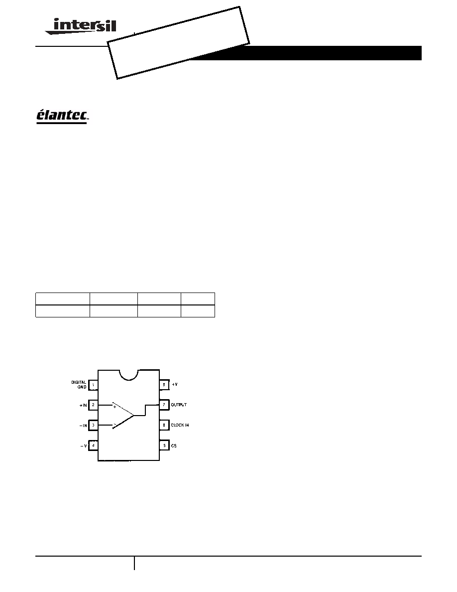
Pinout
EL2019
(8-PIN PDIP)
TOP VIEW
Features
∑ Comparator cannot oscillate
∑ Fast response--5ns data to clock setup, 20ns clock to
output
∑ Wide input differential voltage range--24V on ±15V
supplies
∑ Wide input common mode voltage range--±12V
∑ Precision input stage--V
OS
= 1.5mV
∑ Low input bias current--100nA
∑ Low input offset current--30nA
∑ ±4.5V to ±18V supplies
∑ Three-State TTL compatible output
∑ No supply current glitch during switching
∑ 103dB voltage gain (Low input uncertainty
30µV)
∑ 50% power reduction in shut-down mode
∑ Input and flip-flop remain active in shutdown mode
Applications
∑ Analog to digital converters
∑ ATE pin receiver
∑ Zero crossing detector
∑ Window detector
∑ "Go/no-go" detector
Ordering Information
PART NUMBER
TEMP. RANGE
PACKAGE
PKG. NO.
EL2019CN
-40∞C to +85∞C
8-Pin PDIP
MDP0006
Data Sheet
December 1995, Rev. G
OBS
OLE
TE P
ROD
UCT
NO R
ECO
MME
NDE
D RE
PLAC
EME
NT
cont
act o
ur Te
chni
cal S
uppo
rt Ce
nter
at
1-88
8-INT
ERS
IL or
www.
inter
sil.co
m/ts
c
2
Absolute Maximum Ratings
(T
A
= 25∞C)
V
S
Supply Voltage . . . . . . . . . . . . . . . . . . . . . . . . . . . . . . . .±18V
V
IN
Input Voltage+V
S
to -V
S
V
IN
Differential Input Voltage . . . . Limited only by Power Supplies
I
IN
Input Current (Pins 1, 2 or 3). . . . . . . . . . . . . . . . . . . . ±10mA
I
INS
Input Current (Pins 5 or 6). . . . . . . . . . . . . . . . . . . . . . . ±5mA
P
D
Maximum Power Dissipation
. . . . . . . . . . . . . . . . . . . .1.25W
The maximum power dissipation depends on package type, ambient
temperature and heat sinking. See the Typical Performance curves for more
details.
I
OP
Peak Output Current . . . . . . . . . . . . . . . . . . . . . . . . . . . 50mA
I
O
Continuous Output Current . . . . . . . . . . . . . . . . . . . . . . 25mA
T
A
Operating Temperature Range . . . . . . . . . . . . -40∞C to +85∞C
T
J
Operating Junction Temperature. . . . . . . . . . . . . . . . . . 150∞C
T
ST
Storage Temperature . . . . . . . . . . . . . . . . . . -65∞C to +150∞C
CAUTION: Stresses above those listed in "Absolute Maximum Ratings" may cause permanent damage to the device. This is a stress only rating and operation of the
device at these or any other conditions above those indicated in the operational sections of this specification is not implied.
IMPORTANT NOTE: All parameters having Min/Max specifications are guaranteed. Typical values are for information purposes only. Unless otherwise noted, all tests
are at the specified temperature and are pulsed tests, therefore: T
J
= T
C
= T
A
DC Electrical Specifications
V
S
= ±15V, unless otherwise specified
PARAMETER
DESCRIPTION
TEMP
LIMITS
UNITS
MIN
TYP
MAX
V
OS
Input Offset Voltage
V
CM
= 0V, V
O
Transition Point
25∞C
1.5
6
mV
T
MIN
, T
MAX
8
mV
I
B
Input Bias Current
V
CM
= 0V, Pin 2 or 3
25∞C
±100
±400
nA
T
MIN
, T
MAX
±600
nA
I
OS
Input Offset Current
V
CM
= 0V
25∞C
30
150
nA
T
MIN
, T
MAX
250
nA
CMRR
Common Mode Rejection
Ratio (Note 1)
25∞C
75
90
dB
PSRR
Power Supply Rejection
Ratio (Note 2)
25∞C
75
95
dB
V
CM
Common Mode Input
Range
25∞C
±12
±13
V
T
MIN
, T
MAX
±12
V
V
UNCER
Input Uncertainty Range
30
µV/RMS
V
OL
Output Voltage Logic Low
I
OL
= 8mA and I
OL
= 0mA)
25∞C
-0.05
0.15
0.4
V
T
MIN
, T
MAX
-0.1
0.4
V
V
OH
Output Voltage Logic High
V
S
= ±15V
V
S
= ±15V
V
S
= ±5V
V
S
= ±5V
V
S
= ±5V
25∞C
3.5
4.0
4.65
V
T
MIN
, T
MAX
3.5
4.65
V
25∞C
2.4
V
T
MIN
2.4
V
T
MAX
2.4
V
V
ODIS1
V
OUT
Range, Disabled,
I
OL
= -1mA
V
S
= ±15V
V
S
= ±15V
V
S
= ±5V
25∞C
4.65
V
T
MIN
, T
MAX
4.65
V
25∞C
3.65
V
V
ODIS2
V
OUT
Range, Disabled,
I
OL
= +1mA
V
S
= ±5V to +15V
All
-0.3
-1
V
EL2019
3
V
INH
Clock or CS Inputs
Logic High Input Voltage
25∞C
2
V
T
MIN
, T
MAX
2
V
I
IN
Clock or CS Inputs
Logic Input Current
V
IN
= 0V and V
IN
= 5V
25∞C
±200
µA
T
MIN
, T
MAX
±300
±300
µA
V
INL
Clock or CS Inputs
Logic Low Input Voltage
25∞C
0.8
V
T
MIN
, T
MAX
0.8
V
I
S+EN
Positive Supply
Current Enabled
25∞C
8.8
13
mA
T
MIN
, T
MAX
14
mA
I
S+DIS
Positive Supply
Current Disabled
25∞C
4.9
6
mA
T
MIN
, T
MAX
7
mA
I
S-EN
Negative Supply
Current Enabled
25∞C
14.5
17
mA
T
MIN
, T
MAX
18
mA
I
S-DIS
Negative Supply
Current Disabled
25∞C
6.4
8.0
mA
T
MIN
, T
MAX
8.0
mA
NOTES:
1. V
CM
= +12V to -12V
2. V
S
= ±5V to ±15V
DC Electrical Specifications
V
S
= ±15V, unless otherwise specified (Continued)
PARAMETER
DESCRIPTION
TEMP
LIMITS
UNITS
MIN
TYP
MAX
AC Electrical Specifications
V
S
= ±15V, T
A
= 25∞C
PARAMETER
DESCRIPTION
LIMITS
UNITS
MIN
TYP
MAX
T
S
Setup Time 5mV Overdrive
12
20
ns
T
H
Hold Time
-3
0
ns
T
OPOUT
Clock to Output Delay
20
25
ns
T
OPMIN
Minimum Clock Width
7
ns
T
EN
Output Three-State Enable Delay
40
70
ns
T
DIS
Output Three-State Disable Delay
150
300
ns
EL2019
4
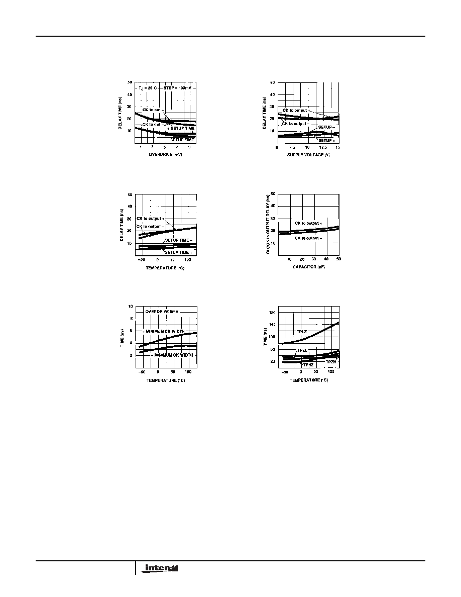
Typical AC Performance Curves
Delay Time vs
Input Overdrive
Delay Time vs
Supply Voltage
Delay Time vs
Temperature
Clock to Output Delay
vs Load Capacitor
Minimum Clock Width
vs Temperature
Enabled/Disabled Times
vs Temperature
EL2019
5
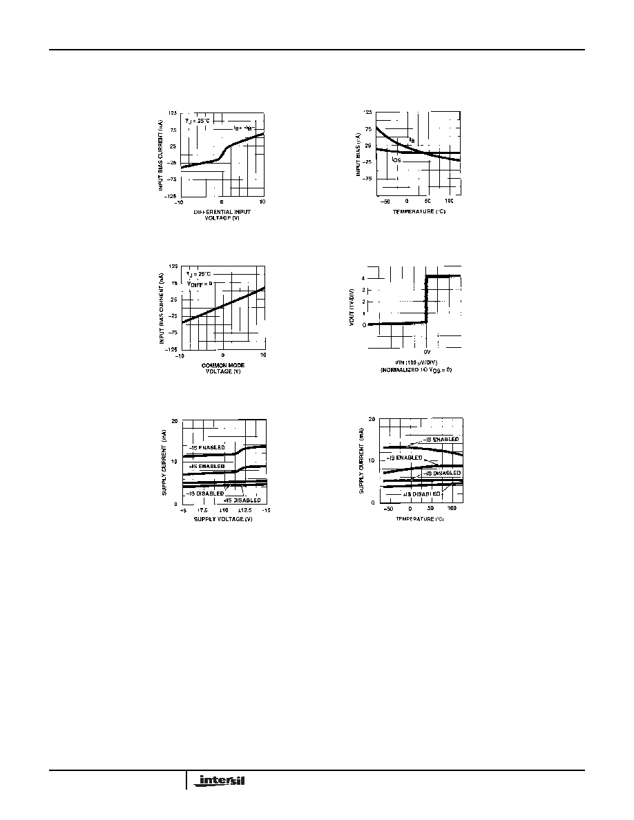
Typical AC Performance Curves
(Continued)
Input Bias Current vs
Differential Input Voltage
Input Bias Current
vs Temperature
Input Bias Current vs
Common Mode Voltage
V
O
/V
I
Transfer Characteristics
Supply Current
vs Supply Voltage
Supply Current
vs Temperature
EL2019