Äîêóìåíòàöèÿ è îïèñàíèÿ www.docs.chipfind.ru
1
®
FN7337.1
CAUTION: These devices are sensitive to electrostatic discharge; follow proper IC Handling Procedures.
1-888-INTERSIL or 321-724-7143
|
Intersil (and design) is a registered trademark of Intersil Americas Inc.
Copyright © Intersil Americas Inc. 2003. All Rights Reserved. Elantec is a registered trademark of Elantec Semiconductor, Inc.
All other trademarks mentioned are the property of their respective owners.
EL5126
8-Channel TFT-LCD Reference Voltage
Generator
The EL5126 is designed to produce
the reference voltages required in
TFT-LCD applications. Each output is
programmed to the required voltage with 10 bits of
resolution. Reference pins determine the high and low
voltages of the output range, which are capable of swinging
to either supply rail. Programming of each output is
performed using the serial interface.
A number of the EL5126 can be stacked for applications
requiring more than 8 outputs. The reference inputs can be
tied to the rails, enabling each part to output the full voltage
range, or alternatively, they can be connected to external
resistors to split the output range and enable finer
resolutions of the outputs.
The EL5126 has 8 outputs and is available in a 32-pin LPP
package. It is specified for operation over the full -40°C to
+85°C temperature range.
Features
· 8-channel reference outputs
· Accuracy of ±0.1%
· Supply voltage of 4.5V to 16.5V
· Digital supply 3.3V to 5V
· Low supply current of 10mA
· Rail-to-rail capability
· I
2
C control interface
Applications
· TFT-LCD drive circuits
· Reference voltage generators
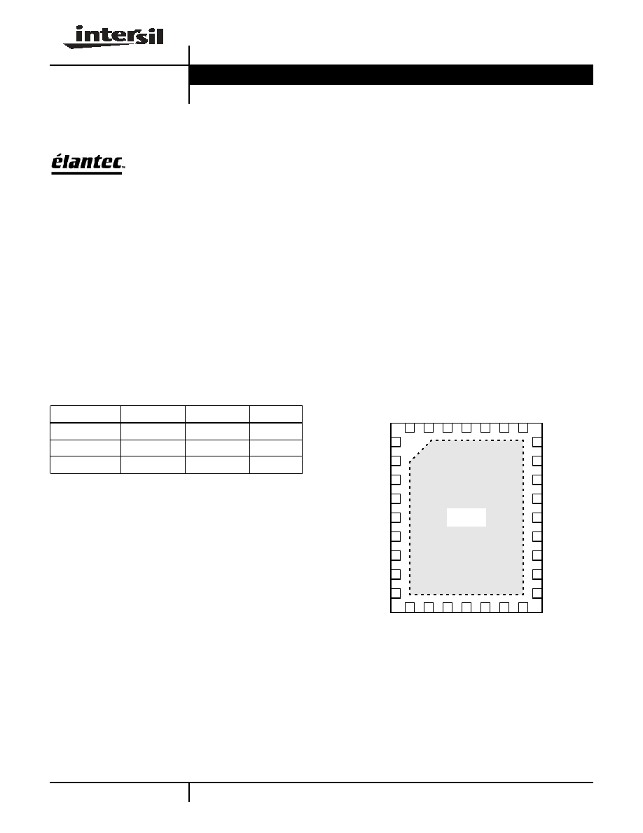
Pinout
EL5126
(32-PIN LPP)
TOP VIEW
Ordering Information
PART NUMBER
PACKAGE
TAPE & REEL
PKG. NO.
EL5126CL
32-Pin LPP
-
MDP0046
EL5126CL-T7
32-Pin LPP
7"
MDP0046
EL5126CL-T13
32-Pin LPP
13"
MDP0046
25
24
23
22
21
20
19
32
31
30
29
28
10
11
12
13
14
1
2
3
4
5
6
7
THERMAL
PAD
VS
VSD
VS
REFH
REFL
AGND
CAP
OUTA
OUTB
OUTC
OUTD
DGND
OUTE
OUTF
OS
C_SEL
OS
C
SDA
SCL
STD/REG
A0
DGND
NC
DGND
NC
8
9
18
17
15
27
16
26
OUTG
OUTH
NC
NC
NC
VS
FI
L
T
ER
NC
THERMAL
PAD
Data Sheet
April 2003
2
Absolute Maximum Ratings
(T
A
= 25
°
C)
Supply Voltage between V
S
and GND. . . . . . . . . . . . . . . . . . . .+18V
Supply Voltage between V
SD
and GND . . . . . . . . . . . . . . . . . . .+7V
Maximum Continuous Output Current . . . . . . . . . . . . . . . . . . . 30mA
Maximum Die Temperature . . . . . . . . . . . . . . . . . . . . . . . . . . +125°C
Storage Temperature . . . . . . . . . . . . . . . . . . . . . . . .-65°C to +150°C
Operating Temperature . . . . . . . . . . . . . . . . . . . . . . .-40°C to +85°C
Power Dissipation . . . . . . . . . . . . . . . . . . . . . . . . . . . . . See Curves
CAUTION: Stresses above those listed in "Absolute Maximum Ratings" may cause permanent damage to the device. This is a stress only rating and operation of the
device at these or any other conditions above those indicated in the operational sections of this specification is not implied.
IMPORTANT NOTE: All parameters having Min/Max specifications are guaranteed. Typical values are for information purposes only. Unless otherwise noted, all tests
are at the specified temperature and are pulsed tests, therefore: T
J
= T
C
= T
A
Electrical Specifications
V
S
= 18V, V
SD
= 5V, V
REFH
= 13V, V
REFL
= 2V, R
L
= 1.5k
and C
L
= 200pF to 0V, T
A
= 25°C Unless
Otherwise Specified.
PARAMETER
DESCRIPTION
CONDITION
MIN
TYP
MAX
UNIT
SUPPLY
I
S
Supply Current
No load
7.6
9
mA
I
SD
Digital Supply Current
1.9
3.2
mA
ANALOG
V
OL
Output Swing Low
Sinking 5mA
50
150
mV
V
OH
Output Swing High
Sourcing 5mA
14.85
14.95
V
I
SC
Short Circuit Current
R
L
= 10
150
240
mA
PSRR
Power Supply Rejection Ratio
V
S
+ is moved from 14V to 16V
45
60
dB
t
D
Program to Out Delay
4
ms
V
AC
Accuracy
20
mV
V
DROOP
Droop Voltage
F
CLOCK
= 25kHz
1
2
mV/ms
R
INH
Input Resistance @ V
REFH
, V
REFL
32
k
REG
Load Regulation
I
OUT
= 5mA step
0.5
1.5
mV/mA
DIGITAL
V
IH
Logic 1 Input Voltage
V
SD
-
20%
V
V
IL
Logic 0 Input Voltage
20%*
V
SD
V
F
CLK
Clock Frequency
400
kHz
R
SDIN
S
DIN
Input Resistance
1
G
t
S
Setup Time
40
ns
t
H
Hold Time
40
ns
t
R
Rise Time
20
ns
t
F
Fall Time
20
ns
EL5126
3
Pin Descriptions
PIN NUMBER
PIN NAME
PIN TYPE
PIN DESCRIPTION
1, 3, 9
VS
Power
Positive power supply for analog circuits
2
VSD
Power
Positive power supply for digital circuits
4
REFH
Analog Input
High reference voltage
5
REFL
Analog Input
Low reference voltage
6, 21, 11, 13
GND
Power
Ground
7
CAP
Analog
Decoupling capacitor for internal reference generator
8, 12, 14, 15, 16, 26
NC
10
A0
Logic Input
Development I
2
C address input, bit 0
17
OUTH
Analog Output
Channel H programmable output voltage
18
OUTG
Analog Output
Channel G programmable output voltage
19
OUTF
Analog Output
Channel F programmable output voltage
20
OUTE
Analog Output
Channel E programmable output voltage
22
OUTD
Analog Output
Channel D programmable output voltage
23
OUTC
Analog Output
Channel C programmable output voltage
24
OUTB
Analog Output
Channel B programmable output voltage
25
OUTA
Analog Output
Channel A programmable output voltage
27
FILTER
Logic Input
Activates internal I
2
C data filter, high = enable, low = disable
28
STD/REG
Logic Input
Selects mode, high = standard, low = register mode
29
SCL
Logic Input
I
2
C clock
30
SDA
Logic Input
I
2
C data input
31
OSC
IP/OP
Oscillator pin for synchronizing multiple chips
32
OSC_SEL
Logic Input
Selects internal/external OSC source, high = external, low = internal
Typical Performance Curves
FIGURE 1. DIFFERENTIAL NONLINEARITY vs CODE
FIGURE 2. SUPPLY VOLTAGE vs SUPPLY CURRENT
0.3
0.2
0.1
0
-0.1
-0.2
-0.3
10
210
410
610
810
1010
INPUT CODE
DIF
F
E
R
ENTIAL N
O
NLINEARITY (LSB)
V
S
=15V
V
SD
=5V
V
REFH
=13V
V
REFL
=2V
7.8
7.4
7.0
6.6
6.4
4
10
12
14
16
18
I
S
(mA)
7.6
7.2
6.8
8
6
ALL CHANNEL OUTPUT = 0V
V
S
(V)
EL5126
4
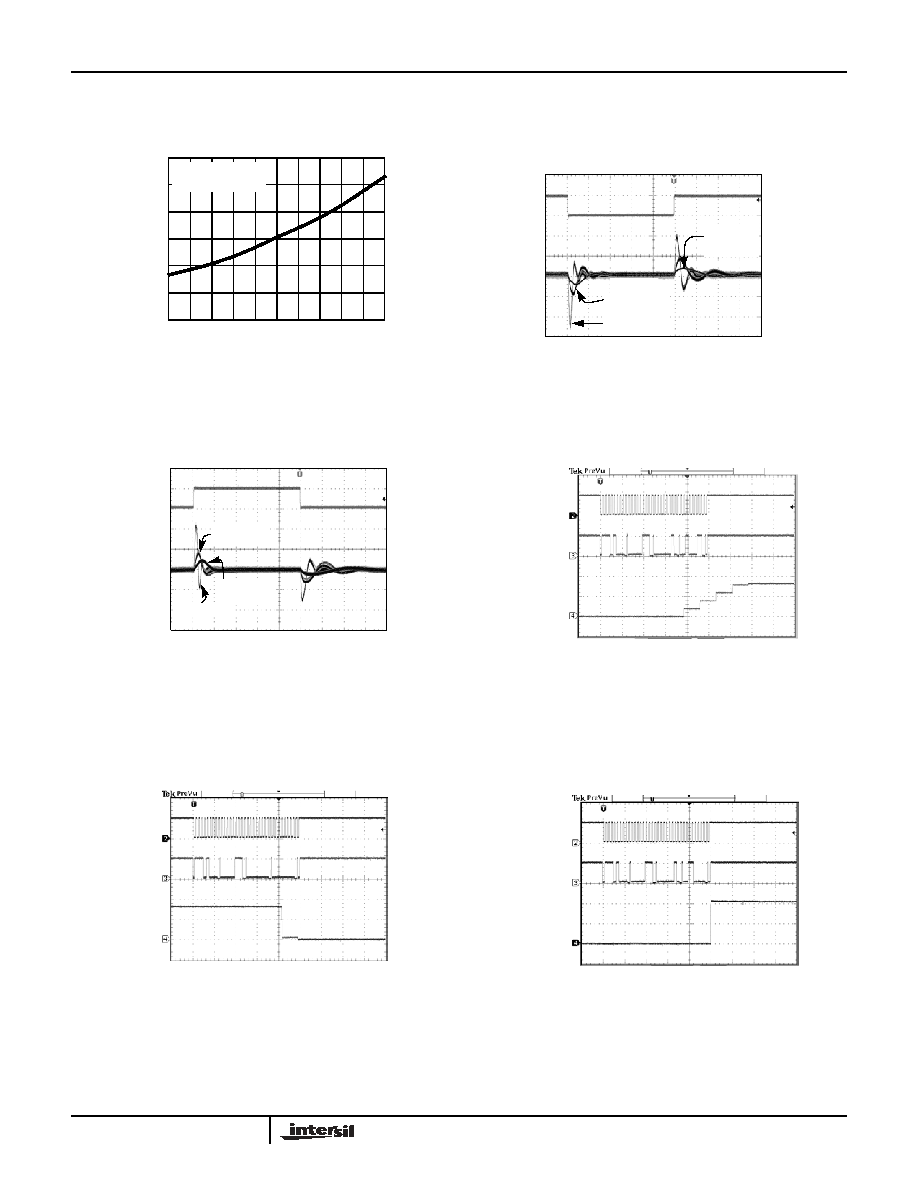
FIGURE 3. DIGITAL SUPPLY VOLTAGE vs DIGITAL SUPPLY
CURRENT
FIGURE 4. TRANSIENT LOAD REGULATION (SOURCING)
FIGURE 5. TRANSIENT LOAD REGULATION (SINKING)
FIGURE 6. LARGE SIGNAL RESPONSE (RISING FROM 0V
TO 8V)
FIGURE 7. LARGE SIGNAL RESPONSE (FALLING FROM 8V
TO 0V)
FIGURE 8. SMALL SIGNAL RESPONSE (RISING FROM 0V
TO 200mV)
Typical Performance Curves
(Continued)
1.2
1.0
0.6
0.2
0
4
4.8 5
I
SD
(mA
)
0.8
0.4
V
S
=V
REFH
=15V
V
REFL
=0V
4.5
4.4
4.2
3
3.8
3.5
3.4
3.2
V
SD
(V)
0mA
5V
5mA/DIV
200mV/DIV
5mA
C
L
=180pF
C
L
=4.7nF
R
S
=20
C
L
=1nF
R
S
=20
V
S
=V
REFH
=15V
M=400ns/DIV
5mA
0mA
C
L
=1nF
R
S
=20
C
L
=180pF
V
S
=V
REFH
=15V
M=400ns/DIV
C
L
=4.7nF
R
S
=20
5V
SDA
0V
OUTPUT
SCLK
0V
5V
0V
10V
5V
M=400µs/DIV
SDA
OUTPUT
SCLK
M=400µs/DIV
SDA
OUTPUT
SCLK
M=400µs/DIV
5V
0V
0V
5V
0V
200mV
EL5126
5
General Description
The EL5126 provides a versatile method of providing the
reference voltages that are used in setting the transfer
characteristics of LCD display panels. The V/T
(Voltage/Transmission) curve of the LCD panel requires that
a correction is applied to make it linear; however, if the panel
is to be used in more than one application, the final curve
may differ for different applications. By using the EL5126,
the V/T curve can be changed to optimize its characteristics
according to the required application of the display product.
Each of the eight reference voltage outputs can be set with a
10-bit resolution. These outputs can be driven to within
50mV of the power rails of the EL5126. As all of the output
buffers are identical, it is also possible to use the EL5126 for
applications other than LCDs where multiple voltage
references are required that can be set to 10 bit accuracy.
Digital Interface
The EL5126 uses a simple two-wire I
2
C digital interface to
program the outputs. The bus line SCLK is the clock signal
line and bus SDA is the data information signal line. The
EL5126 can support the clock rate up to 400kHz. External
pull up resistor is required for each bus line. The typical
value for these two pull up resistor is about 1k
.
START AND STOP CONDITION
The Start condition is a high to low transition on the SDA line
while SCLK is high. The Stop condition is a low to high
transition on the SDA line while SCLK is high. The start and
stop conditions are always generated by the master. The
bus is considered to be busy after the start condition and to
be free again a certain time after the stop condition. The two
bus lines must be high when the buses are not in use. The
I
2
C Timing Diagram 2 shows the format.
FIGURE 9. SMALL SIGNAL RESPONSE (FALLING FROM
200mV TO 0V)
FIGURE 10. POWER DISSIPATION vs AMBIENT
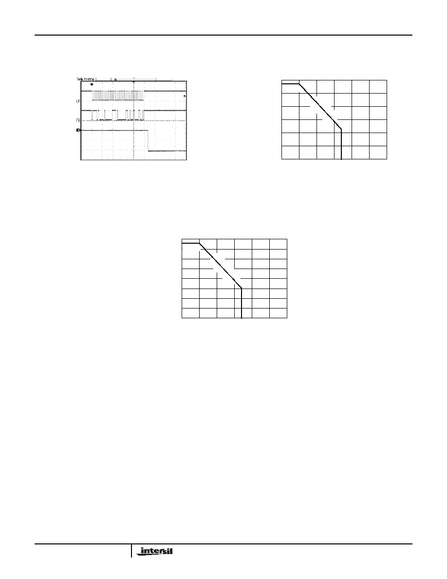
TEMPERATURE
FIGURE 11. POWER DISSIPATION vs AMBIENT TEMPERATURE
Typical Performance Curves
(Continued)
SDA
OUTPUT
SCLK
M=400µs/DIV
JEDEC JESD51-7 HIGH EFFECTIVE THERMAL
CONDUCTIVITY TEST BOARD - LPP EXPOSED
DIEPAD SOLDERED TO PCB PER JESD51-5
3
2.5
2
1.5
1
0.5
0
0
25
50
75
100
150
AMBIENT TEMPERATURE (°C)
POWER DISS
IP
A
T
ION
(W)
2.857W
125
85
JA
=3
5°C
/W
LP
P3
2
JEDEC JESD51-3 AND SEMI G42-88
(SINGLE LAYER) TEST BOARD
0.8
0.7
0.5
0.3
0.2
0.1
0
0
25
50
75
100
150
AMBIENT TEMPERATURE (°C)
POWER DISS
IP
A
T
ION
(W)
758mW
125
85
0.6
0.4
JA
=1
32
°C
/W
LP
P3
2
EL5126