1
®
FN7004.3
EL5224, EL5324, EL5424
12MHz Rail-to-Rail Buffers + 100mA V
COM
Amplifier
The EL5224, EL5324, and EL5424 feature 8, 10, and 12 low
power buffers, respectively, and one high power output
amplifier. They are designed primarily for buffering column
driver reference voltages in TFT-LCD applications as well as
generation of the V
COM
supply. Each low power buffer
features a -3dB bandwidth of 12MHz and features rail-to-rail
input/output capability. The high power buffer can drive
100mA and swings to within 2V of each rail.
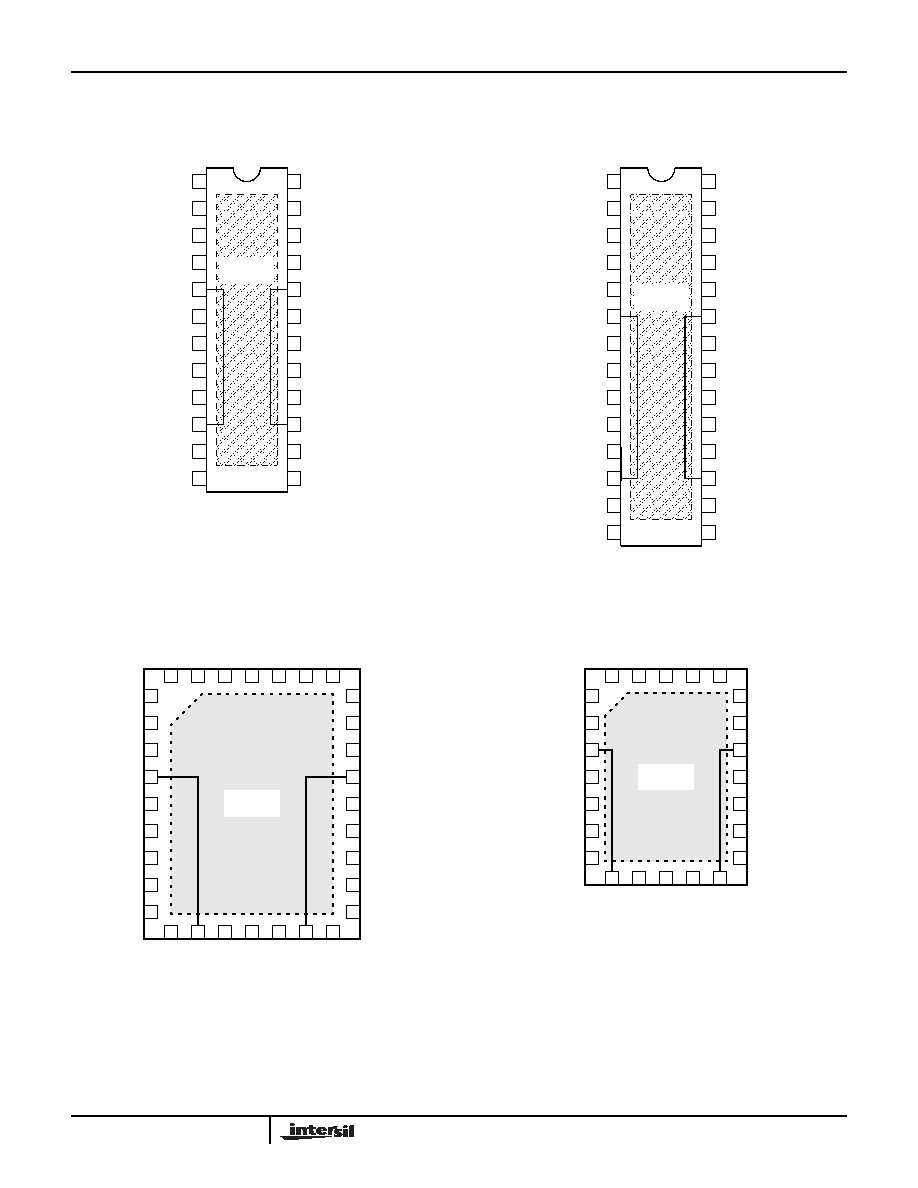
The 8-channel EL5224 is available in 24-pin QFN and 24-pin
HTSSOP packages, the 10-channel EL5324 is available in
32-pin QFN and 28-pin HTSSOP packages, and the
12-channel EL5434 is available in the 32-pin QFNQFN
package. They are specified for operation over the full -40°C
to +85°C temperature range.
Features
· 8, 10, and 12 channel versions
· 12MHz -3dB buffer bandwidth
· 150mA V
COM
buffer
· Operating supply voltage from 4.5V to 16.5V
· Low supply current - 6mA total (8-channel version)
· Rail-to-rail input/output swing (buffers only)
· QFN package - just 0.9mm high
· Pb-Free available (RoHS compliant)
Applications
· TFT-LCD column driver buffering and V
COM
supply
· Electronics notebooks
· Computer monitors
· Electronics games
· Touch-screen displays
· Portable instrumentation
Ordering Information
PART NUMBER
PACKAGE
TAPE &
REEL
PKG. DWG. #
EL5224IL
24-Pin QFN
MDP0046
EL5224IL-T7
24-Pin QFN
7"
MDP0046
EL5224IL-T13
24-Pin QFN
13"
MDP0046
EL5224ILZ
(See Note)
24-Pin QFN
(Pb-free)
MDP0046
EL5224ILZ-T7
(See Note)
24-Pin QFN
(Pb-free)
7"
MDP0046
EL5224ILZ-T13
(See Note)
24-Pin QFN
(Pb-free)
13"
MDP0046
EL5224IRE
24-Pin HTSSOP
-
MDP0048
EL5224IRE-T7
24-Pin HTSSOP
7"
MDP0048
EL5224IRE-T13
24-Pin HTSSOP
13"
MDP0048
EL5224IREZ
(See Note)
24-Pin HTSSOP
(Pb-free)
-
MDP0048
EL5224IREZ-T7
(See Note)
24-Pin HTSSOP
(Pb-free)
7"
MDP0048
EL5224IREZ-T13
(See Note)
24-Pin HTSSOP
(Pb-free)
13"
MDP0048
EL5324IL
32-Pin QFN
MDP0046
EL5324IL-T7
32-Pin QFN
7"
MDP0046
EL5324IL-T13
32-Pin QFN
13"
MDP0046
EL5324ILZ
(See Note)
32-Pin QFN
(Pb-free)
MDP0046
EL5324ILZ-T7
(See Note)
32-Pin QFN
(Pb-free)
7"
MDP0046
EL5324ILZ-T13
(See Note)
32-Pin QFN
(Pb-free)
13"
MDP0046
EL5324IRE
28-Pin HTSSOP
-
MDP0048
EL5324IRE-T7
28-Pin HTSSOP
7"
MDP0048
EL5324IRE-T13
28-Pin HTSSOP
13"
MDP0048
EL5324IREZ
(See Note)
28-Pin HTSSOP
(Pb-free)
-
MDP0048
EL5324IREZ-T7
(See Note)
28-Pin HTSSOP
(Pb-free)
7"
MDP0048
EL5324IREZ-T13
(See Note)
28-Pin HTSSOP
(Pb-free)
13"
MDP0048
EL5424IL
32-Pin QFN
MDP0046
EL5424IL-T7
32-Pin QFN
7"
MDP0046
EL5424IL-T13
32-Pin QFN
13"
MDP0046
EL5424ILZ
(See Note)
32-Pin QFN
(Pb-free)
MDP0046
EL5424ILZ-T7
(See Note)
32-Pin QFN
(Pb-free)
7"
MDP0046
EL5424ILZ-T13
(See Note)
32-Pin QFN
(Pb-free)
13"
MDP0046
NOTE: Intersil Pb-free products employ special Pb-free material sets; molding
compounds/die attach materials and 100% matte tin plate termination finish,
which are RoHS compliant and compatible with both SnPb and Pb-free soldering
operations. Intersil Pb-free products are MSL classified at Pb-free peak reflow
temperatures that meet or exceed the Pb-free requirements of IPC/JEDEC J
STD-020.
Ordering Information
(Continued)
PART NUMBER
PACKAGE
TAPE &
REEL
PKG. DWG. #
Data Sheet
May 11, 2005
CAUTION: These devices are sensitive to electrostatic discharge; follow proper IC Handling Procedures.
1-888-INTERSIL or 1-888-352-6832
|
Intersil (and design) is a registered trademark of Intersil Americas Inc.
Copyright Intersil Americas Inc. 2003, 2005. All Rights Reserved
All other trademarks mentioned are the property of their respective owners.
3
NOTE: All parameters having Min/Max specifications are guaranteed. Typ values are for information purposes only. Unless otherwise noted, all tests
are at the specified temperature and are pulsed tests, therefore: T
J
= T
C
= T
A
Absolute Maximum Ratings
(T
A
= 25°C)
Supply Voltage between V
S
+ and V
S
- . . . . . . . . . . . . . . . . . . . .+18V
Input Voltage . . . . . . . . . . . . . . . . . . . . . . . . . . V
S
- -0.5V, V
S
+ +0.5V
Maximum Continuous Output Current (V
OUT0-9
) . . . . . . . . . . 30mA
Maximum Continuous Output Current (V
OUTA
). . . . . . . . . . . 150mA
Power Dissipation . . . . . . . . . . . . . . . . . . . . . . . . . . . . . See Curves
Maximum Die Temperature . . . . . . . . . . . . . . . . . . . . . . . . . . +125°C
Storage Temperature . . . . . . . . . . . . . . . . . . . . . . . .-65°C to +150°C
Ambient Operating Temperature . . . . . . . . . . . . . . . .-40°C to +85°C
CAUTION: Stresses above those listed in "Absolute Maximum Ratings" may cause permanent damage to the device. This is a stress only rating and operation of the
device at these or any other conditions above those indicated in the operational sections of this specification is not implied.
Electrical Specifications
V
S
+ = +15V, V
S
- = 0, R
L
= 10k
, R
F
= R
G
= 20k
, C
L
= 10pF to 0V, Gain of V
COM
= -1, and T
A
= 25°C Unless
Otherwise Specified
PARAMETER
DESCRIPTION
CONDITIONS
MIN
TYP
MAX
UNIT
INPUT CHARACTERISTICS (REFERENCE BUFFERS)
V
OS
Input Offset Voltage
V
CM
= 0V
2
14
mV
TCV
OS
Average Offset Voltage Drift
(Note 1)
5
µV/
°C
I
B
Input Bias Current
V
CM
= 0V
2
50
nA
R
IN
Input Impedance
1
G
C
IN
Input Capacitance
1.35
pF
A
V
Voltage Gain
1V
V
OUT
14V
0.992
1.008
V/V
INPUT CHARACTERISTICS (V
COM
BUFFER)
V
OS
Input Offset Voltage
V
CM
= 7.5V
1
4
mV
TCV
OS
Average Offset Voltage Drift
(Note 1)
3
µV/
°C
I
B
Input Bias Current
V
CM
= 7.5V
2
100
nA
R
IN
Input Impedance
1
G
C
IN
Input Capacitance
1.35
pF
V
REG
Load Regulation
V
COM
= 6V, -100mA < I
L
< 100mA
-20
+20
mV
OUTPUT CHARACTERISTICS (REFERENCE BUFFERS)
V
OL
Output Swing Low
I
L
= 7.5mA
50
150
mV
V
OH
Output Swing High
I
L
= 7.5mA
14.85
14.95
V
I
SC
Short Circuit Current
120
140
mA
OUTPUT CHARACTERISTICS (V
COM
BUFFER)
V
OL
Output Swing Low
50
to 7.5V
1
1.5
V
V
OH
Output Swing High
50
to 7.5V
13.5
14
V
I
SC
Short Circuit Current
160
mA
POWER SUPPLY PERFORMANCE
PSRR
Power Supply Rejection Ratio
Reference buffer V
S
from 5V to 15V
55
80
dB
V
COM
buffer, V
S
from 5V to 15V
60
100
dB
I
S
Total Supply Current
EL5224 (no load)
5
6.8
8
mA
EL5324 (no load)
6
7.8
9.5
mA
EL5424 (no load)
7
8.8
11
mA
DYNAMIC PERFORMANCE (BUFFER AMPLIFIERS)
SR
Slew Rate (Note 2)
-4V
V
OUT
4V, 20% to 80%
7
15
V/µs
t
S
Settling to +0.1% (A
V
= +1)
(A
V
= +1), V
O
= 2V step
250
ns
BW
-3dB Bandwidth
R
L
= 10k
, C
L
= 10pF
12
MHz
EL5224, EL5324, EL5424
5
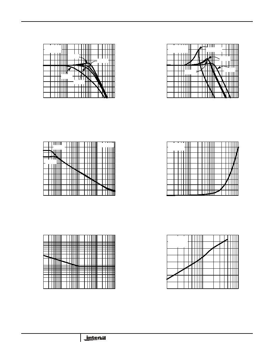
Typical Performance Curves
FIGURE 1. FREQUENCY RESPONSE FOR VARIOUS R
L
(BUFFER)
FIGURE 2. FREQUENCY RESPONSE FOR VARIOUS C
L
(BUFFER)
FIGURE 3. PSRR vs FREQUENCY (BUFFER)
FIGURE 4. OUTPUT IMPEDANCE vs FREQUENCY (BUFFER)
FIGURE 5. INPUT NOISE SPECIAL DENSITY vs FREQUENCY
(BUFFER)
FIGURE 6. OVERSHOOT vs LOAD CAPACITANCE (BUFFER)
NORM
ALIZE
D
MAGN
ITUDE
(dB)
20
10
0
-10
-20
-30
100K
1M
10M
100M
FREQUENCY (Hz)
V
S
=±7.5V
C
L
=10pF
10k
562
150
1k
NORM
ALIZE
D
MAGN
ITUDE
(dB)
20
10
0
-10
-20
-30
100K
1M
10M
100M
FREQUENCY (Hz)
V
S
=±7.5V
R
L
=10k
100pF
1000pF
12pF
47pF
PS
R
R
(
d
B)
100
80
60
40
20
0
1K
10K
1M
10M
FREQUENCY (Hz)
V
S
=±7.5V
PSRR-
PSRR+
100K
OUTP
UT IM
PE
DANCE (
)
600
480
360
240
120
0
100K
1M
10M
100M
FREQUENCY (Hz)
V
S
=±7.5V
T
A
=25°C
VO
L
T
A
G
E
N
OIS
E
(nV
/
Hz)
100
10
1
10K
100K
10M
100M
FREQUENCY (Hz)
1M
80
70
60
50
40
20
0
10
100
1K
CAPACITANCE (pF)
OV
ERS
H
OO
T (%
)
30
10
V
S
=±7.5V
R
L
=10k
V
IN
=100mV
EL5224, EL5324, EL5424